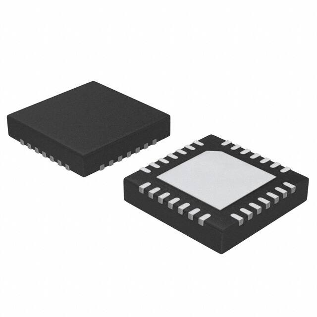
A3969 Dual Full-Bridge PWM Motor Driver
Features and Benefits
▪ ▪ ▪ ▪ ▪ ▪ ▪ ▪ ±650 mA Continuous Output Current 30 V Output Voltage Rating Internal Fixed-Frequency PWM Current Control Satlington Sink Drivers User-Selectable Blanking Window Internal Ground-Clamp and Flyback Diodes Internal Thermal-Shutdown Circuitry Crossover-Current Protection and UVLO Protection
Description
The A3969 is designed to drive both windings of a two-phase bipolar stepper motor. The device includes two H-bridges capable of continuous output currents of ±650 mA and operating voltages to 30 V. Motor winding current can be controlled by the internal fixed-frequency, pulse-width modulated (PWM), current-control circuitry. The peak load current limit is set by the user’s selection of a reference voltage and current-sensing resistors. The fixed-frequency pulse duration is set by a user-selected external RC timing network. The capacitor in the RC timing network also determines a user-selectable blanking window that prevents false triggering of the PWM current-control circuitry during switching transitions. To reduce on-chip power dissipation, the H-bridge power outputs have been optimized for low saturation voltages. The sink drivers feature the Allegro® patented Satlington® output structure. The Satlington outputs combine the low voltage drop of a saturated transistor and the high peak current capability of a Darlington.
Continued on the next page…
Package: 28 pin QFN (suffix ET)
Continued on the next page… Approximate scale
Typical Application
+3.3 V +24 V +3.3 V 20 kΩ 10 kΩ
56 kΩ
680 pF
47 μF
28
27
26
25
24
23
22
21 20 19 0.5 Ω 18 17 16 EN1 PH1 15
0.5 Ω
1 2 3 4 5 LOGIC LOGIC
EN2 PH2
6 7
VBB
10
12
13
DS3969
14
11
8
9
�A3969
Dual Full-Bridge PWM Motor Driver
and flyback diodes, and crossover-current protection. The A3969 is supplied in a 28-pin QFN lead (Pb) free plastic package with exposed thermal pad and 100% matte tin leadframe plating. It has a 5 x 5 mm footprint and 0.90 mm nominal height.
Description (continued) For each bridge, a PHASE input controls load-current polarity by selecting the appropriate source and sink driver pair. For each bridge, an ENABLE input, when held high, disables the output drivers. Special power-up sequencing is not required. Internal circuit protection includes thermal shutdown with hysteresis, ground-clamp
Selection Guide
73 pieces/tube Tape, 3000 pieces/reel *Contact Allegro for additional packing options
Part Number A3969SET-T A3969SETTR-T
Packing*
Package 5 x 5 mm QFN, 28 pin
Absolute Maximum Ratings
Characteristic Load Supply Voltage Symbol VBB Peak Output Current IOUT Continuous. Output current rating may be limited by duty cycle, ambient temperature, and heat sinking. Under any set of conditions, do not exceed the specified current rating or a junction temperature of 150°C. Notes Rating 30 ±750 ±650 7 -0.3 to VCC + 0.3 0.45 Range S –20 to 85 150 –55 to 150 Units V mA mA V V V ºC ºC ºC
Logic Supply Voltage Input Voltage Sense Voltage Operating Ambient Temperature Maximum Junction Temperature Storage Temperature
VCC Vin VS TA TJ(max) Tstg
Thermal Characteristics* (additional data available on Allegro Web site)
Characteristic Package Thermal Resistance, Junction-to-Ambient Package Thermal Resistance, Junction-to-Tab Package Power Dissipation Symbol RθJA RθJT PD(max) RθJA = 32 °C/W, TA = 25°C Notes 4-layer PCB, based on JEDEC standard Rating 32 2 3.9 Units °C/W °C/W W
* Per SEMI G42-88 Specification, Thermal Test Board Standardization for Measuring Junction-to-Ambient Thermal Resistance of Semiconductor Packages.
Allegro MicroSystems, Inc. 115 Northeast Cutoff, Box 15036 Worcester, Massachusetts 01615-0036 (508) 853-5000 www.allegromicro.com
2
�A3969
Dual Full-Bridge PWM Motor Driver
Functional Block Diagram
VCC
OUT 1A
OUT1B
OUT 2A
OUT 2B
VBB
PH1 V BB
PH2
UVLO & TSD
CONTROL LOGIC1
CONTROL LOGIC2
UVLO & TSD
EN1 CURRENT-SENSE COMPARATOR 1 CURRENT-SENSE COMPARATOR 2
EN2
SOURCE ENABLE 1
PWM LATCH 1 R Q S
BLANKING GATE 1
+ –
+ –
BLANKING GATE 2
PWM LATCH 2 R Q S
SOURCE ENABLE 2
÷4
OSC
GND
RC
SENSE 1 R1S
SENSE 2 R2S
REF
Dwg. FP-036-7
RT
CT
28 OUT2B
26 VCC
NC SENSE2
1 2 3 4 5 6 7 NC 10 8 9
VBB
22 VBB 21 OUT1B 20 NC 19 SENSE1 18 NC 17 GND 16 EN1 15 PH1 NC 14
24 REF NC 12
Pin-out Diagram
NC GND NC EN2 PH2
LOGIC
LOGIC
OUT1A 13
OUT2A
GND 11
NC
23 NC
27 NC
25 RC
Allegro MicroSystems, Inc. 115 Northeast Cutoff, Box 15036 Worcester, Massachusetts 01615-0036 (508) 853-5000 www.allegromicro.com
3
�A3969
Dual Full-Bridge PWM Motor Driver
ELECTRICAL CHARACTERISTICS at TA = +25°C, VBB = 30 V, VCC = 3.0 V to 3.6 V, VREF = 1.7 V, VS = 0 V, 56 kΩ and 680 pF RC to Ground (unless noted otherwise)
Limits Characteristic Output Drivers
Load Supply Voltage Range Output Leakage Current VBB ICEX Operating, IOUT = ±650 mA, L = 3 mH VOUT = 30 V VOUT = 0 V Source Driver, IOUT = -400 mA Output Saturation Voltage VCE(SAT) Source Driver, IOUT = -650 mA Sink Driver, IOUT = +400 mA, VS = 0.425 V Sink Driver, IOUT = +650 mA, VS = 0.425 V Clamp Diode Forward Voltage Motor Supply Current (No Load) VF IBB(ON) IBB(OFF) IF = 400 mA IF = 650 mA VENABLE1 = VENABLE2 = 0.8 V VENABLE1 = VENABLE2 = 2.4 V 5 — — — — — — — — — — —
很抱歉,暂时无法提供与“A3969SETTR-T”相匹配的价格&库存,您可以联系我们找货
免费人工找货