A3974
DMOS Dual Full-Bridge PWM Motor Driver
Last Time Buy
These parts are in production but have been determined to be
LAST TIME BUY. This classification indicates that the product is
obsolete and notice has been given. Sale of this device is currently
restricted to existing customer applications. The device should not be
purchased for new design applications because of obsolescence in the
near future. Samples are no longer available.
Date of status change: November 2, 2009
Deadline for receipt of LAST TIME BUY orders: April 30, 2010
Recommended Substitutions:
For existing customer transition, and for new customers or new applications, refer to the A3992.
NOTE: For detailed information on purchasing options, contact your
local Allegro field applications engineer or sales representative.
Allegro MicroSystems, Inc. reserves the right to make, from time to time, revisions to the anticipated product life cycle plan
for a product to accommodate changes in production capabilities, alternative product availabilities, or market demand. The
information included herein is believed to be accurate and reliable. However, Allegro MicroSystems, Inc. assumes no responsibility for its use; nor for any infringements of patents or other rights of third parties which may result from its use.
�A3974
DMOS Dual Full-Bridge PWM Motor Driver
Features and Benefits
Description
▪ ±1.5 A, 50 V continuous output rating
▪ Low rDS(on) DMOS output drivers
▪ Programmable slow, fast, and mixed current-decay modes
▪ Serial-interface controls chip functions
▪ Synchronous rectification for low power dissipation
▪ Internal UVLO and thermal shutdown circuitry
▪ Crossover-current protection
▪ Sleep and idle modes
Designed for pulse width modulated (PWM) current control
of two DC motors, the A3974 is capable of output currents to
±1.5 A and operating voltages to 50 V. Internal fixed off-time
PWM current-control timing circuitry can be programmed via
a serial interface to operate in slow, fast, and mixed currentdecay modes.
Independent ENABLE input terminals are provided for use
in controlling the speed and torque of each DC motor with
externally applied PWM control signals.
Synchronous rectification circuitry allows the load current
to flow through the low rDS(on) of the DMOS output driver
during the current decay. This feature will eliminate the need
for external clamp diodes in most applications, saving cost
and external component count, while minimizing power
dissipation.
Package: 44-pin PLCC with internally
fused pins (suffix ED)
Internal circuit protection includes thermal shutdown with
hysteresis, undervoltage monitoring of VDD and the charge
pump, and crossover-current protection. Special power-up
sequencing is not required.
Not to scale
The A3974 is supplied in a 44-pin plastic PLCC with 3 internally
fused pins on each side, for maximum heat dissipation. The fused
pins are at ground potential and need no electrical isolation.
ENABLE1
NC
OUT1B
42
41
40
GND
LOAD
43 SUPPLY1
GND
1
GND
2
44
NC
SENSE1
4
NC
5
3
OUT1A
6
Pin-out Diagram
VBB1
NC
7
STROBE
8
CP2
37
CP1
36
CP
GND 11
35
GND
GND 12
34
GND
GND 13
33
GND
CLOCK
9
DATA 10
PROGRAM
PWM TIMER
CHARGE PUMP
NC
38
SERIAL PORT
39
LOGIC
REF1 14
REF2 15
LOGIC
16
SUPPLY
NC
PROGRAM
PWM TIMER
LOGIC
VDD
17
32
OSC
31
SLEEP
30
VREG
29
NC
29319.35C
OUT2B 28
NC 27
25
ENABLE2 26
LOAD
SUPPLY2
23
GND 24
GND
GND 22
21
NC 20
SENSE2
NC 19
OUT2A 18
VBB2
Dwg. PP-073
�A3974
DMOS Dual Full-Bridge PWM Motor Driver
Selection Guide
Part Number
A3974SED-T
A3974SEDTR-T
Packing
27 pieces per tube
450 pieces per reel
Absolute Maximum Ratings
Characteristic
Symbol
Notes
Rating
Units
Load Supply Voltage
VBB
50
V
Logic Supply Voltage
VDD
7.0
V
Logic Input Voltage Range
VIN
Continuous
–0.3 to VDD+ 0.3
V
Pulsed, tw < 30 ns
–1.0 to VDD+ 1.0
V
Reference Voltage
Sense Voltage (DC)
Output Current
VREF
VS
IOUT
3
V
Continuous
0.5
V
Pulsed, tw < 1 μs
2.5
V
Output current rating may be limited by duty
cycle, ambient temperature, and heat sinking.
Under any set of conditions, do not exceed the
specified current rating or a junction temperature
of 150°C.
±1.5
A
Operating Ambient Temperature
TA
–20 to 85
ºC
Maximum Junction Temperature
TJ(max)
150
ºC
Tstg
–55 to 150
ºC
Storage Temperature
Range S
Thermal Characteristics may require derating at maximum conditions, see application information
Characteristic
Package Thermal Resistance
Test Conditions*
Symbol
RθJA
4-layer PCB based on JEDEC standard
RθJT
Value Units
22
ºC/W
6
ºC/W
*Additional thermal information available on the Allegro website.
Allegro MicroSystems, Inc.
115 Northeast Cutoff
Worcester, Massachusetts 01615-0036 U.S.A.
1.508.853.5000; www.allegromicro.com
2
�A3974
DMOS Dual Full-Bridge PWM Motor Driver
FUNCTIONAL BLOCK DIAGRAM
VBB1
VDD
UNDERVOLTAGE &
FAULT DETECT
CP2
CP1
CHARGE PUMP
BANDGAP
VDD
CREG
TSD
CP
+
LOGIC
SUPPLY
LOAD
SUPPLY1
CHARGE
PUMP
BANDGAP
REGULATOR
ENABLE1
OUT1A
GATE DRIVE
PHASE
SYNC RECT MODE
SYNC RECT DISABLE
MODE
CONTROL LOGIC
VREG
OUT1B
SENSE1
CS1
ZERO CURRENT DETECT
FIXED OFF
PROGRAMMABLE BLANK
DECAY
RS1
PWM TIMER
CURRENT SENSE
FIXED OFF
ENABLE2
PHASE
ENABLE
SYNC RECT MODE
SYNC RECT DISABLE
PWM MODE INT
PWM MODE EXT
PROGRAMMABLE BLANK
DECAY
PWM TIMER
SLEEP
MODE
REFERENCE
BUFFER &
DIVIDER
SERIAL
PORT
REF1
VREF
LOAD
SUPPLY2
CHARGE
PUMP
+
VBB2
OUT2A
GATE DRIVE
OSC
CLOCK
DATA
STROBE
OUT2B
CONTROL LOGIC
SENSE2
TO PWM TIMER
CS2
ZERO CURRENT DETECT
RS2
CURRENT SENSE
REFERENCE
BUFFER &
DIVIDER
REF2
VREF2
Dwg. FP-048-1
Copyright © 2001 Allegro MicroSystems, Inc.
Allegro MicroSystems, Inc.
115 Northeast Cutoff
Worcester, Massachusetts 01615-0036 U.S.A.
1.508.853.5000; www.allegromicro.com
3
�A3974
DMOS Dual Full-Bridge PWM Motor Driver
ELECTRICAL CHARACTERISTICS at TA = +25°C, VBB = 50 V, VDD = 5.0 V, fPWM < 50 kHz (unless
otherwise noted).
Characteristic
Symbol
Test Conditions
Min.
Limits
Typ. Max.
Units
Output Drivers
Load Supply Voltage Range
Output Leakage Current
Output ON Resistance
Body Diode Forward Voltage
Load Supply Current
VBB
IDSS
rDS(on)
VF
IBB
Operating
15
—
50
V
During sleep mode
0
—
50
V
VOUT = VBB
—
很抱歉,暂时无法提供与“A3974SEDTR”相匹配的价格&库存,您可以联系我们找货
免费人工找货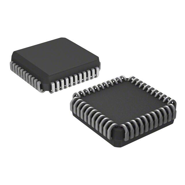


 工商网监
湘ICP备2023018690号
工商网监
湘ICP备2023018690号