A3979 Microstepping DMOS Driver with Translator
Features and Benefits
▪ ▪ ▪ ▪ ▪ ▪ ▪ ▪ ▪ ±2.5 A, 35 V output rating Low RDS(On) outputs: 0.28 Ω source, 0.22 Ω sink, typical Automatic current decay mode detection/selection 3.0 to 5.5 V logic supply voltage range Slow, Fast or Mixed current decay modes Home output Synchronous rectification for low power dissipation Internal UVLO and thermal shutdown circuitry Crossover-current protection
Description
The A3979 is a complete microstepping motor driver with built-in translator, designed as a pin-compatible replacement for the successful A3977, with enhanced microstepping (1/16 step) precision. It is designed to operate bipolar stepper motors in full-, half-, quarter-, and sixteenth-step modes, with an output drive capacity of up to 35 V and ±2.5 A. The A3979 includes a fixed off-time current regulator that has the ability to operate in Slow, Fast, or Mixed decay modes. This current-decay control scheme results in reduced audible motor noise, increased step accuracy, and reduced power dissipation. The translator is the key to the easy implementation of the A3979. It allows the simple input of one pulse on the STEP pin to drive the motor one microstep, which can be either a full step, half, quarter, or sixteenth, depending on the setting of the MS1 and MS2 logic inputs. There are no phase-sequence tables, high-frequency control lines, or complex interfaces to program. The A3979 interface is an ideal fit for applications where a complex microprocessor is unavailable or is overburdened. Internal synchronous-rectification control circuitry is provided to improve power dissipation during PWM operation. Internal circuit protection includes: thermal shutdown with hysteresis, UVLO (undervoltage lockout), and crossover-current protection. Special power-on sequencing is not required.
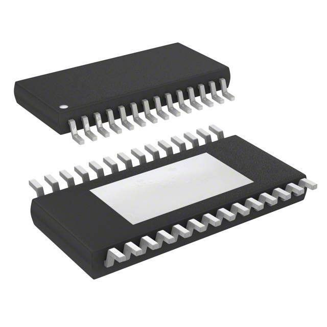
Package: 28 lead TSSOP (suffix LP) with exposed thermal pad
Not to scale
The A3979 is supplied in a low-profile (height ≤1.20 mm), 28-pin TSSOP with exposed thermal pad. The package is lead (Pb) free, with 100% matte tin leadframe plating.
Pin-out Diagram
SENSE1 1 HOME 2 DIR 3 OUT1A 4 PFD 5 RC1 6 AGND 7 REF 8 RC2 9 VDD 10 OUT2A 11 MS2 12 MS1 13 SENSE2 14 ÷8
PWM Timer Charge Pump
28 VBB1 27 SLEEP 26 ENABLE 25 OUT1B 24 CP2 Translator and Control Logic 23 CP1 22 VCP 21 PGND Reg 20 VREG 19 STEP 18 OUT2B 17 RESET 16 SR 15 VBB2
AGND and PGND must be connected together externally
26184.23D
�A3979
DMOS Microstepping Driver with Translator
Selection Guide
Part Number A3979SLP-T A3979SLPTR-T Packing 50 pieces per tube 4000 pieces per reel
Absolute Maximum Ratings
Load Supply Voltage Output Current Logic Supply Voltage Logic Input Voltage Range Sense Voltage Reference Voltage Operating Ambient Temperature Junction Temperature Storage Temperature VBB IOUT VDD VIN VSENSE VREF TA TJ(max) Tstg Range S tW > 30 ns tW < 30 ns Output current rating may be limited by duty cycle, ambient temperature, and heat sinking. Under any set of conditions, do not exceed the specified current rating or a junction temperature of 150°C. 35 ±2.5 7.0 –0.3 to VDD + 0.3 –1 to VDD + 1 0.5 VDD –20 to 85 150 –55 to 150 V A V V V V V °C °C °C
Allegro MicroSystems, Inc. 115 Northeast Cutoff, Box 15036 Worcester, Massachusetts 01615-0036 (508) 853-5000 www.allegromicro.com
2
�A3979
DMOS Microstepping Driver with Translator
Functional Block Diagram
0.22 µF
0.22 µF
VREG Logic Supply VDD UVLO and Fault Regulator Bandgap 2V
CP2
CP1
Charge Pump VCP
Reference Supply REF DAC DMOS Full Bridge
0.22 µF Load Supply VBB1 >47 µF 4 OUT1A OUT1B PWM Timer: PWM Latch Blanking Mixed Decay Gate Drive 4 Control Logic DMOS Full Bridge VBB2
RC1 STEP RT1 CT1 DIR RESET MS1 MS2 HOME SLEEP SR ENABLE VPFD PFD 0.1 µF RC2 PWM Timer: PWM Latch Blanking Mixed Decay OUT2A OUT2B Translator
SENSE1 RS1 CS1
SENSE2
RT2
CT2
DAC
RS2
CS2
Exposed Thermal Pad AGND PGND
(Required)
Allegro MicroSystems, Inc. 115 Northeast Cutoff, Box 15036 Worcester, Massachusetts 01615-0036 (508) 853-5000 www.allegromicro.com
3
�A3979
DMOS Microstepping Driver with Translator
ELECTRICAL CHARACTERISTICS at TA = 25°C, VBB = 35 V, VDD = 3.0 to 5.5 V (unless otherwise noted)
Characteristics Output Drivers Load Supply Voltage Range Output Leakage Current2 Output On Resistance Body Diode Forward Voltage Symbol Test Conditions Operating During Sleep mode VOUT = VBB VOUT = 0 V Source driver, IOUT = –2.5 A Sink driver, IOUT = 2.5 A Source diode, IF = –2.5 A Sink diode, IF = 2.5 A fPWM < 50 kHz Operating, outputs disabled Sleep mode Operating fPWM < 50 kHz Outputs off Sleep mode Min. 8 0 – – – – – – – – – 3.0 – – – 0.7× VDD – VIN = 0.7 × VDD VIN = 0.3 × VDD Operating –20 –20 0 – 0.7× VDD – – – VREF = 2 V, Phase Current = 38.27% VREF = 2 V, Phase Current = 70.71% VREF = 2 V, Phase Current = 100.00% RT = 56 kΩ, CT = 680 pF RT = 56 kΩ, CT = 680 pF Synchronous rectification enabled – – – 1 700 30 100 Typ.1 – –