A3982
DMOS Stepper Motor Driver with Translator
Features and Benefits
Description
▪ Low RDS(on) outputs
▪ Automatic current decay mode detection/selection
▪ Mixed and Slow current decay modes
▪ Synchronous rectification for low power dissipation
▪ Internal UVLO and thermal shutdown circuitry
▪ Crossover-current protection
The A3982 is a complete stepper motor driver with builtin translator for easy operation. It is designed to operate
bipolar stepper motors in full- and half-step modes, with an
output drive capacity of up to 35 V and ±2 A. The A3982
includes a fixed off-time current regulator which has the
ability to operate in Slow or Mixed decay modes.
The translator is the key to the easy implementation of the
A3982. Simply inputting one pulse on the STEP input drives
the motor one step. There are no phase sequence tables, high
frequency control lines, or complex interfaces to program.
The A3982 interface is an ideal fit for applications where a
complex microprocessor is unavailable or is overburdened.
The chopping control in the A3982 automatically selects
the current decay mode (Slow or Mixed). When a signal
occurs at the STEP input pin, the A3982 determines if
that step results in a higher or lower current in each of the
motor phases. If the change is to a higher current, then the
decay mode is set to Slow decay. If the change is to a lower
current, then the current decay is set to Mixed (set initially
to a fast decay for a period amounting to 31.25% of the
Package: 24 pin SOICW with internally
fused leads (suffix LB)
Continued on the next page…
Not to scale
Pin-out Diagram
OUT2A
1
24 OUT1A
SENSE2
2
23 SENSE1
22 VBB1
4
21 OUT1B
ENABLE
5
20 DIR
PGND
6
PGND
7
CP1
8
CP2
9
MS1 12
26184.28C
19 PGND
18 PGND
17 REF
16 STEP
15 VDD
OSC
VREG 11
Reg
VCP 10
Translator
& Control Logic
3
Charge
Pump
VBB2
OUT2B
14 ROSC
13 RESET
�A3982
DMOS Stepper Motor Driver with Translator
Description (continued)
fixed off-time, then to a slow decay for the remainder of the
off-time). This current decay control scheme results in reduced
audible motor noise, increased step accuracy, and reduced power
dissipation.
Internal synchronous rectification control circuitry is provided to
improve power dissipation during PWM operation.
Internal circuit protection includes: thermal shutdown with
hysteresis, undervoltage lockout (UVLO), and crossover-current
protection. Special power-on sequencing is not required.
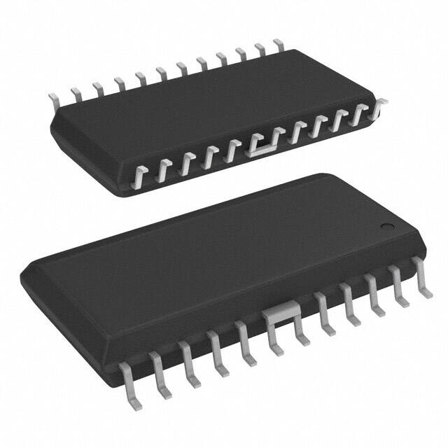
The A3982 is supplied in a 24-pin wide-body SOIC
(package LB) with internally-fused power ground leads for
enhanced thermal dissipation. It is lead (Pb) free, with 100%
matte tin plated leadframe.
Selection Guide
Part Number
Packing*
A3982SLB-T
31 pieces per tube
A3982SLBTR-T
1000 pieces per reel
Package
24-pin Wide SOIC with pins 6 and 7, and 18
and 19, fused internally
*Contact Allegro for additional packing options
Absolute Maximum Ratings
Rating
Units
Load Supply Voltage
Characteristic
VBB
35
V
Logic Input Voltage
VIN
–0.3 to 7
V
Sense Voltage
Symbol
Notes
VSENSE
0.5
V
Reference Voltage
VREF
4
V
Output Current
IOUT
±2
A
–20 to 85
ºC
Output current rating may be limited by duty cycle,
ambient temperature, and heat sinking. Under
any set of conditions, do not exceed the specified
current rating or a junction temperature of 150°C.
Range S
Operating Ambient Temperature
TA
Maximum Junction Temperature
TJ(max)
150
ºC
Tstg
–55 to 150
ºC
Storage Temperature
Allegro MicroSystems, LLC
115 Northeast Cutoff
Worcester, Massachusetts 01615-0036 U.S.A.
1.508.853.5000; www.allegromicro.com
2
�A3982
DMOS Stepper Motor Driver with Translator
Functional Block Diagram
0.1 μF
0.22 μF
VREG
VDD
Current
Regulator
ROSC
CP1
CP2
Charge
Pump
OSC
VCP
0.1 μF
REF
DMOS Full Bridge
DAC
VBB1
OUT1A
OUT1B
PWM Latch
Blanking
Mixed Decay
STEP
DIR
RESET
SENSE1
Gate
Drive
Translator
MS1
Control
Logic
DMOS Full Bridge
RS1
VBB2
OUT2A
OUT2B
PWM Latch
Blanking
Mixed Decay
ENABLE
SENSE2
RS2
DAC
VREF
Allegro MicroSystems, LLC
115 Northeast Cutoff
Worcester, Massachusetts 01615-0036 U.S.A.
1.508.853.5000; www.allegromicro.com
3
�A3982
DMOS Stepper Motor Driver with Translator
ELECTRICAL CHARACTERISTICS1 at TA = 25°C, VBB = 35 V (unless otherwise noted)
Characteristics
Output Drivers
Load Supply Voltage Range
Logic Supply Voltage Range
Output On Resistance
Min.
Typ.2
Max.
Units
8
3.0
–
–
–
–
–
–
–
–
–
–
0.370
0.330
–
–
–
–
–
–
35
5.5
0.460
0.380
1.2
1.2
4
2
8
5
V
V
Ω
Ω
V
V
mA
mA
mA
mA
VIN(1)
VDD0.7
–
–
V
VIN(0)
–
–
V
μA
Symbol
VBB
VDD
RDSON
Body Diode Forward Voltage
VF
Motor Supply Current
IBB
Logic Supply Current
IDD
Test Conditions
Operating
Operating
Source Driver, IOUT = –1.5 A
Sink Driver, IOUT = 1.5 A
Source Diode, IF = –1.5 A
Sink Diode, IF = 1.5 A
fPWM < 50 kHz
Operating, outputs disabled
fPWM < 50 kHz
Outputs off
Control Logic
Logic Input Voltage
Logic Input Current
Input Hysteresis
Blank Time
IIN(1)
IIN(0)
VIN = VDD0.7
VIN = VDD0.3
VHYS(IN)
tBLANK
Fixed Off-Time
tOFF
Reference Input Voltage Range
Reference Input Current
VREF
IREF
Current Trip-Level Error3
errI
Crossover Dead Time
Protection
Thermal Shutdown Temperature
Thermal Shutdown Hysteresis
UVLO Enable Threshold
UVLO Hysteresis
tDT
OSC > 3 V
ROSC = 25 kΩ
VREF = 2 V, %ITripMAX = 70.71%
VREF = 2 V, %ITripMAX = 100.00%
TJ
TJHYS
UVLO
UVHYS
VDD rising
–20
很抱歉,暂时无法提供与“A3982SLBTR-T”相匹配的价格&库存,您可以联系我们找货
免费人工找货