A3988
Quad DMOS Full Bridge PWM Motor Driver
FEATURES AND BENEFITS
•
•
•
•
•
•
•
•
•
•
DESCRIPTION
36 V output rating
4 full bridges
Dual stepper motor driver
High current outputs
3.3 and 5 V compatible logic supply
Synchronous rectification
Internal undervoltage lockout (UVLO)
Thermal shutdown circuitry
Crossover-current protection
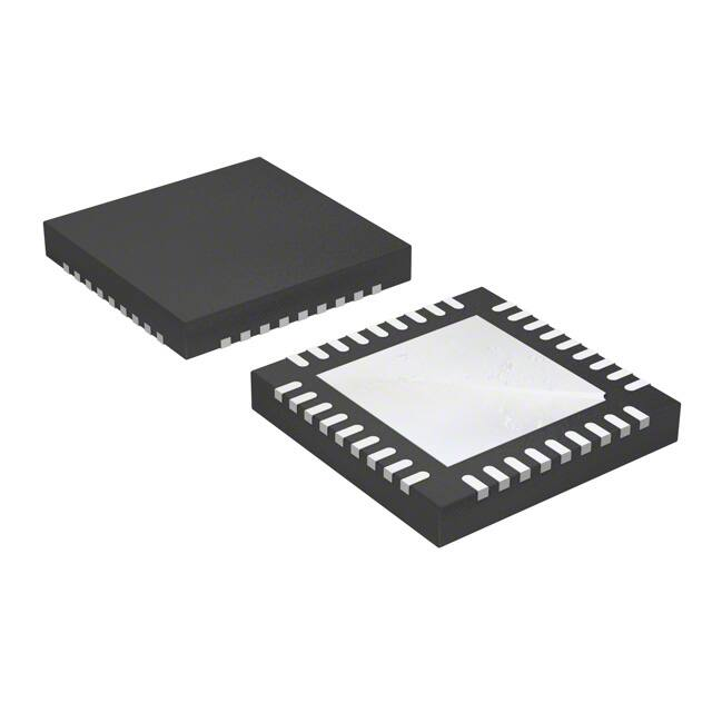
Low profile QFN package
The A3988 is a quad DMOS full-bridge driver capable of driving
up to two stepper motors or four DC motors. Each full-bridge
output is rated up to 1.2 A and 36 V. The A3988 includes fixed
off-time pulse width modulation (PWM) current regulators,
along with 2- bit nonlinear DACs (digital-to-analog converters)
that allow stepper motors to be controlled in full, half, and
quarter steps, and DC motors in forward, reverse, and coast
modes. The PWM current regulator uses the Allegro™ patented
mixed decay mode for reduced audible motor noise, increased
step accuracy, and reduced power dissipation.
Internal synchronous rectification control circuitry is provided
to improve power dissipation during PWM operation.
Packages
Protection features include thermal shutdown with hysteresis,
undervoltage lockout (UVLO) and crossover current protection.
Special power up sequencing is not required.
Package EV, 36 pin QFN
0.90 mm nominal height
with exposed thermal pad
The A3988 is supplied in two packages, EV and JP, with exposed
power tabs for enhanced thermal performance. The EV is a
6 mm x 6 mm, 36 pin QFN package with a nominal overall
package height of 0.90 mm. The JP is a 7 mm × 7 mm 48 pin
LQFP. Both packages are lead (Pb) free, with 100% matte tin
leadframe plating.
Approximate scale
Package JP, 48 pin LQFP
with exposed thermal pad
Microprocessor
I12
PHASE3
I03
I13
PHASE4
I04
I14
VREF1
VREF
VREF2
VREF3
VREF4
VDD 3.3 V
VDD
A3988
OUT2A
OUT2B
OUT3A
Bipolar Stepper Motors
OUT3B
OUT4A
OUT4B
SENSE2
SENSE1
SENSE3
SENSE4
Typical Application Circuit
A3988DS, Rev. 10
0.22 µF
50 V
OUT1B
I11
I02
100 µF
50 V
OUT1A
I01
PHASE2
VMOTOR 32 V
VBB2
VCP
CP2
CP1
PHASE1
VBB1
0.1 µF
50 V
0.1 µF
50 V
RS2
RS1
RS3
RS4
�A3988
Quad DMOS Full Bridge PWM Motor Driver
Selection Guide
Part Number
Package
Packing
A3988SEV-T
36 pin QFN with exposed thermal pad
61 pieces per tube
A3988SEVTR-T
36 pin QFN with exposed thermal pad
1500 pieces per reel
A3988SJPTR-T
48 pin LQFP with exposed thermal pad
1500 pieces per reel
SPECIFICATIONS
Absolute Maximum Ratings
Characteristic
Symbol
Load Supply Voltage
VBB
Logic Supply Voltage
VDD
Output Current
IOUT
Logic Input Voltage Range
VIN
Notes
Pulsed tw < 1 µs
May be limited by duty cycle, ambient temperature, and heat sinking. Under
any set of conditions, do not exceed the specified current rating or a Junction
Temperature of 150°C.
Pulsed tw < 1 µs
SENSEx Pin Voltage
VSENSEx
Pulsed tw < 1 µs
VREFx Pin Voltage
Operating Temperature Range
Junction Temperature
Storage Temperature Range
VREFx
Rating
Units
-0.5 to 36
V
38
V
–0.4 to 7
V
1.2
A
2.8
A
–0.3 to 7
V
0.5
V
2.5
V
2.5
V
–20 to 85
ºC
TJ(max)
150
ºC
Tstg
–40 to 125
ºC
TA
Range S
Thermal Characteristics (may require derating at maximum conditions)
Characteristic
Symbol
Package Thermal Resistance
RθJA
Test Conditions
Min.
Units
EV package, 4 layer PCB based on JEDEC standard
27
ºC/W
JP package, 4 layer PCB based on JEDEC standard
23
ºC/W
Power Dissipation versus Ambient Temperature
5500
5000
JP Package
4-layer PCB
(RθJA = 23 ºC/W)
4500
Power Dissipation, PD (mW)
4000
3500
3000
2500
2000
1500
EV Package
4-layer PCB
(RθJA = 27 ºC/W)
1000
500
0
25
50
75
100
125
Temperature (°C)
150
175
Allegro MicroSystems, LLC
115 Northeast Cutoff
Worcester, Massachusetts 01615-0036 U.S.A.
1.508.853.5000; www.allegromicro.com
2
�A3988
Quad DMOS Full Bridge PWM Motor Driver
0.1 µF
50 V
0.1 µF
50 V
0.22 µF
50 V
VBB1
VCP
CP2
CP1
100 µF
50 V
VDD
DMOS
FULL-BRIDGE 1
VBB1
VCP
OSC
CHARGE PUMP
OUT1A
PHASE1
OUT1B
I01
Control Logic
Bridges 1 and 2
I11
PHASE2
SENSE1
I02
GATE
DRIVE
VREF1
3
+
Sense1
VBB1
DMOS
FULL-BRIDGE 2
-
I12
PWM Latch
BLANKING
OUT2A
3
PWM Latch
BLANKING
OUT2B
-
Sense2
+
VREF2
PHASE3
VCP
I03
Sense2
Control Logic
Bridges 3 and 4
I13
SENSE2
VBB2
PHASE4
DMOS
FULL-BRIDGE 3
I04
OUT3A
OUT3B
I14
GATE
DRIVE
VREF3
3
Sense3
PWM Latch
BLANKING
DMOS
FULL-BRIDGE 4
Sense4
OUT4B
SENSE4
GND
-
Sense4
PWM Latch
BLANKING
GND
3
OUT4A
+
VREF4
SENSE3
VBB2
+
Sense3
Functional Block Diagram
Allegro MicroSystems, LLC
115 Northeast Cutoff
Worcester, Massachusetts 01615-0036 U.S.A.
1.508.853.5000; www.allegromicro.com
3
�A3988
19 I14
20 OUT4A
21 SENSE4
22 OUT4B
23 VBB2
24 OUT3B
25 SENSE3
26 OUT3A
27 I13
25 NC
26 NC
27 OUT4A
28 SENSE4
29 OUT4B
30 NC
31 VBB2
32 OUT3B
34 OUT3A
35 NC
36 NC
Pin-out Diagrams and Terminal List Table
33 SENSE3
Quad DMOS Full Bridge PWM Motor Driver
I13 37
24
I14
I12 38
23
NC
I11 39
22
PHASE1
GND 40
21
PHASE2
20
GND
19
VREF4
I12 28
18
PHASE1
NC 41
I11 29
17
PHASE2
VCP 42
GND 30
16
GND
CP1 43
18
VREF3
VCP 31
15
VREF4
CP2 44
17
VREF2
14
VREF3
I01 45
16
VREF1
15
VDD
PAD
CP1 32
PAD
Package EV, 36-Pin QFN Pin-out
9
SENSE2
NC 12
8
OUT2B
NC 11
7
NC
OUT2A 10
6
4
SENSE1
VBB1
3
OUT1A
5
2
OUT1B
1
NC
9
PHASE4
Packages are not to scale
NC
8
PHASE3
OUT2A
10
7
PHASE4
I03 36
SENSE2
13
6
I04 48
OUT2B
VDD
5
11
VBB1
PHASE3
I02 35
4
14
OUT1B
I03 47
3
VREF1
SENSE1
12
2
I01 34
1
VREF2
I04
13
OUT1A
CP2 33
I02 46
Package JP, 48-Pin LQFP Pin-out
Terminal List Table
EV
2
3
4
5
6
7
8
9
10
11
12
13
14
15
16
17
18
19
20
21
22
23
24
25
26
27
28
29
30
31
32
33
34
35
36
1
–
–
1VBB1
Number
JP
3
4
5
6
8
9
10
13
14
15
16
17
18
19
20
21
22
24
27
28
29
31
32
33
34
37
38
39
40
42
43
44
45
46
47
48
1, 2, 7, 11,
12, 23, 25,
26, 30, 35,
36, 41
–
Pin Name
Pin Description
OUT1A
SENSE1
OUT1B
VBB11
OUT2B
SENSE2
OUT2A
PHASE4
PHASE3
VDD
VREF1
VREF2
VREF3
VREF4
GND
PHASE2
PHASE1
I14
OUT4A
SENSE4
OUT4B
VBB21
OUT3B
SENSE3
OUT3A
I13
I12
I11
GND
VCP
CP1
CP2
I01
I02
I03
I04
DMOS Full-Bridge 1 Output A
Sense Resistor Terminal for Bridge 1
DMOS Full-Bridge 1 Output B
Load Supply Voltage
DMOS Full-Bridge 2 Output B
Sense Resistor Terminal for Bridge 2
DMOS Full-Bridge 2 Output A
Control Input
Control Input
Logic Supply Voltage
Analog Input
Analog Input
Analog Input
Analog Input
Ground
Control Input
Control Input
Control Input
DMOS Full-Bridge 4 Output A
Sense Resistor Terminal for Bridge 4
DMOS Full-Bridge 4 Output B
Load Supply Voltage
DMOS Full-Bridge 3 Output B
Sense Resistor Terminal for Bridge 3
DMOS Full-Bridge 3 Output A
Control Input
Control Input
Control Input
Ground
Reservoir Capacitor Terminal
Charge Pump Capacitor Terminal
Charge Pump Capacitor Terminal
Control Input
Control Input
Control Input
Control Input
NC
No Connect
PAD
Exposed pad for enhanced thermal
performance. Should be soldered to the
PCB.
and VBB2 need to be connected together close to the A3988
Allegro MicroSystems, LLC
115 Northeast Cutoff
Worcester, Massachusetts 01615-0036 U.S.A.
1.508.853.5000; www.allegromicro.com
4
�A3988
Quad DMOS Full Bridge PWM Motor Driver
ELECTRICAL CHARACTERISTICS1: valid at TA = 25°C, VBB = 36 V, unless otherwise noted
Min.
Typ.2
Max.
Units
Load Supply Voltage Range
Characteristics
VBB
Operating
8.0
–
36
V
Logic Supply Voltage Range
VDD
Operating
3.0
–
5.5
V
VDD Supply Current
IDD
–
7
10
mA
Source driver, IOUT = –1.2 A, TJ = 25°C
–
700
800
mΩ
–
700
800
mΩ
IOUT = 1.2 A
–
–
1.3
V
–20
–
20
µA
–
–
8
mA
VIN(1)
0.7×VDD
–
–
V
VIN(0)
–
–
0.3×VDD
V
–20
很抱歉,暂时无法提供与“A3988SEVTR-1-T”相匹配的价格&库存,您可以联系我们找货
免费人工找货