A4931
3-Phase Brushless DC Motor Pre-Driver
Features and Benefits
Description
▪ Drives 6 N-channel MOSFETs
▪ Synchronous rectification for low power dissipation
▪ Internal UVLO and thermal shutdown circuitry
▪ Hall element inputs
▪ PWM current limiting
▪ Dead time protection
▪ FG outputs
▪ Standby mode
▪ Lock detect protection
▪ Overvoltage protection
The A4931 is a complete 3-phase brushless DC motor pre-driver.
The device is capable of driving a wide range of N-channel
power MOSFETs and can support motor supply voltages up to
30 V. Commutation logic is determined by three Hall-element
inputs spaced at 120°.
Other features include fixed off-time pulse width modulation
(PWM) current control for limiting inrush current, locked-rotor
protection with adjustable delay, thermal shutdown, overvoltage
monitor, and synchronous rectification. Internal synchronous
rectification reduces power dissipation by turning on the
appropriate MOSFETs during current decay, thus shorting
the body diode with the low RDS(on) MOSFET. Overvoltage
protection disables synchronous rectification when the motor
pumps the supply voltage beyond the overvoltage threshold
during current recirculation.
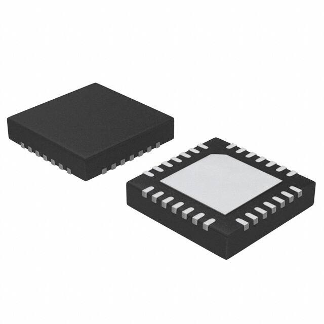
Package: 28-contact QFN (ET package)
The A4931 offers enable, direction, and brake inputs that can
control current using either phase or enable chopping. Logic
outputs FG1 and FG2 can be used to accurately measure motor
rotation. Output signals toggle state during Hall transitions,
providing an accurate speed output to a microcontroller or
speed control circuit.
Approximate Scale 1:1
Operating temperature range is –20°C to 105°C. The A4931
is supplied in a 5 mm × 5 mm, 28-terminal QFN package with
exposed thermal pad. This small footprint package is lead (Pb)
free with 100% matte tin leadframe plating.
Typical Application
0.1 μF
0.1 μF
0.1 μF 2 kΩ
VIN
CLD HBIAS
CP1
CP2 VCP VBB
VIN
GHA
SA
GLA
M
FG1
A4931
System
Control
Logic
FG2
BRAKEZ
ENABLE
DIR
GHB
SB
GLB
GHC
SC
GLC
SENSE
GND HA+ HA– HB+ HB– HC+ HC–
4931-DS, Rev. 6
0.1 μF
�A4931
3-Phase Brushless DC Motor Pre-Driver
Selection Guide
Part Number
A4931METTR-T
Packing
Package
1500 pieces per reel
5 mm x 5 mm, 0.90 mm nominal height QFN
Absolute Maximum Ratings
Characteristic
Load Supply Voltage
Symbol
Notes
VBB
Motor Phase Output
SX
tw < 500 ns
Hall Input
VHx
DC
Logic Input Voltage Range
VIN
Units
38
V
–3
V
–0.3 to 7
V
–0.3 to 7
V
Operating Ambient Temperature
TA
–20 to 105
ºC
Maximum Junction Temperature
TJ(max)
150
ºC
Tstg
–40 to 150
ºC
Rating
Units
32
ºC/W
2
ºC/W
Storage Temperature
Range M
Rating
Thermal Characteristics
Characteristic
Symbol
Package Thermal Resistance, Junction
RθJA
to Ambient
Package Thermal Resistance, Junction
RθJP
to Exposed Pad
*For additional information, refer to the Allegro website.
Test Conditions*
4-layer PCB based on JEDEC standard
Allegro MicroSystems, LLC
115 Northeast Cutoff
Worcester, Massachusetts 01615-0036 U.S.A.
1.508.853.5000; www.allegromicro.com
2
�A4931
3-Phase Brushless DC Motor Pre-Driver
Functional Block Diagram
0.1 μF
CLD
Lock
Detect
CP1
CP2
0.1 μF
FG1
VCP
CHARGE PUMP
0.1 μF
HBIAS
2 kΩ
HA+
HALL
HA-
HB+
HALL
VIN
Enable
0.1 μF
VBB
VREG
OVP
VCP
Communication
Logic
VREG
GHA
SA
HB-
GHB
SB
GLB
GATE
DRIVE
HC+
HALL
HC-
GHC
SC
GLC
Control
Logic
FG1
FG2
GLA
BRAKEZ
SENSE
System
Logic
DIR
RSENSE
200 mV
ENABLE
VIN
GND
Terminal List
Number
Name
1
HA+
2
HA -
3
4
5
6
Description
Number
Name
Description
Hall input A
15
GLB
Low side gate drive B
Hall input A
16
GLA
Low side gate drive A
HB+
Hall input B
17
GHC
High side gate drive C
HB -
Hall input B
18
SC
HC+
Hall input C
19
GHB
HC-
Hall input C
20
SB
7
GND
Ground
21
GHA
8
HBIAS
Hall bias power supply output
22
SA
9
CP1
Charge pump capacitor terminal
23
FG1
10
CP2
Charge pump capacitor terminal
24
FG2
FG 2 speed control output (ΦA input)
11
VBB
Supply voltage
25
CLD
Locked rotor detect timing capacitor
12
VCP
Reservoir capacitor terminal
26
DIR
13
SENSE
Sense resistor connection
27
ENABLE
Logic input – external PWM control
14
GLC
Low side gate drive C
28
BRAKEZ
Logic input – motor brake (active low)
High side source connection C
High side gate drive B
High side source connection B
High side gate drive A
High side source connection A
FG 1 speed control output (3 Φ inputs)
Logic input – motor direction
Allegro MicroSystems, LLC
115 Northeast Cutoff
Worcester, Massachusetts 01615-0036 U.S.A.
1.508.853.5000; www.allegromicro.com
3
�A4931
3-Phase Brushless DC Motor Pre-Driver
ELECTRICAL CHARACTERISTICS* Valid at TA= 25°C, VBB = 24 V, unless noted otherwise
Characteristics
Supply Voltage Range
Motor Supply Current
Symbol
VBB
IBB
Test Conditions
Min.
Typ.
Max.
Operating
8
–
VBBOV
V
fPWM < 30 kHz, CLOAD = 1000 pF
–
5
6
mA
–
3
3.5
mA
7.2
7.5
7.8
V
IHBIASlim
30
–
–
mA
VIN(1)
2
–
–
V
VIN(0)
–
–
0.8
V
HBIAS
VHBIAS
HBIAS Current Limit
Charge pump on, outputs disabled, Standby mode
Units
0 mA ≤ IHBIAS ≤ 24 mA
Control Logic
Logic Input Voltage
Logic Input Current
Input Pin Glitch Reject
IIN(1)
VIN = 2 V
–1
tlock / 2
The Lock Detect function can be disabled by connecting CLD to
GND.
When the A4931 is in Brake mode, the Lock Detect counter is
disabled.
Allegro MicroSystems, LLC
115 Northeast Cutoff
Worcester, Massachusetts 01615-0036 U.S.A.
1.508.853.5000; www.allegromicro.com
8
�A4931
3-Phase Brushless DC Motor Pre-Driver
ET Package, 28-Contact QFN
0.30
5.00 ±0.15
1.15
28
1
2
0.50
28
1
A
5.00 ±0.15
3.15
4.80
3.15
29X
D
SEATING
PLANE
0.08 C
C
4.80
C
+0.05
0.25 –0.07
PCB Layout Reference View
0.90 ±0.10
0.50
For Reference Only
(reference JEDEC MO-220VHHD-1)
Dimensions in millimeters
Exact case and lead configuration at supplier discretion within limits shown
+0.20
0.55 –0.10
A Terminal #1 mark area
B
3.15
2
1
28
3.15
B Exposed thermal pad (reference only, terminal #1
identifier appearance at supplier discretion)
C Reference land pattern layout (reference IPC7351
QFN50P500X500X100-29V1M);
All pads a minimum of 0.20 mm from all adjacent pads; adjust as
necessary to meet application process requirements and PCB layout
tolerances; when mounting on a multilayer PCB, thermal vias at the
exposed thermal pad land can improve thermal dissipation (reference
EIA/JEDEC Standard JESD51-5)
D Coplanarity includes exposed thermal pad and terminals
Copyright ©2007-2013, Allegro MicroSystems, LLC
Allegro MicroSystems, LLC reserves the right to make, from time to time, such departures from the detail specifications as may be required to
permit improvements in the performance, reliability, or manufacturability of its products. Before placing an order, the user is cautioned to verify that
the information being relied upon is current.
Allegro’s products are not to be used in life support devices or systems, if a failure of an Allegro product can reasonably be expected to cause the
failure of that life support device or system, or to affect the safety or effectiveness of that device or system.
The information included herein is believed to be accurate and reliable. However, Allegro MicroSystems, LLC assumes no responsibility for its
use; nor for any infringement of patents or other rights of third parties which may result from its use.
For the latest version of this document, visit our website:
www.allegromicro.com
Allegro MicroSystems, LLC
115 Northeast Cutoff
Worcester, Massachusetts 01615-0036 U.S.A.
1.508.853.5000; www.allegromicro.com
9
�
很抱歉,暂时无法提供与“A4931MET-T”相匹配的价格&库存,您可以联系我们找货
免费人工找货