A4938
3-Phase Brushless DC Motor Pre-Driver
Features and Benefits
Description
▪ Drives 6 N-channel MOSFETs
▪ Synchronous rectification for low power dissipation
▪ Internal UVLO and thermal shutdown circuitry
▪ Hall element inputs
▪ PWM current limiting
▪ Dead time protection
▪ FG outputs
▪ Standby mode
▪ Lock detect protection
▪ Overvoltage protection
The A4938 is a complete 3-phase brushless DC (BLDC) motor
pre-driver, supplying direct, high-current gate drive of an all
N-channel power MOSFET 3-phase bridge. The device has
three Hall-element inputs, a sequencer for commutation control,
fixed off-time pulse width modulation (PWM) current control,
and locked-rotor detection.
Output current is scaled by the capability of the external
MOSFETs. Locked rotor detection delay is set by an external
capacitor on the CLD terminal. The ENABLE, DIR, and
BRAKEZ inputs can be used to control motor speed, position,
and torque. Motor speed can be determined using the FG1
output.
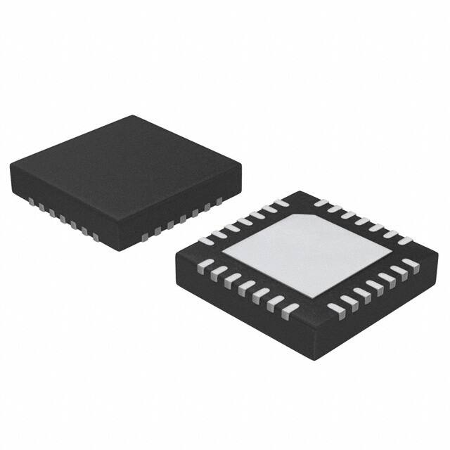
Package: 28-contact QFN (ET package)
The external MOSFETS can be PWMed using an external
signal on the PWM input, or using the internal PWM current
regulator. In either case, the A4938 synchronous rectification
feature reduces power dissipation by turning on the appropriate
MOSFETs during current decay.
The Hall elements can be inexpensive types, when used with
noise filtering to prevent false commutation signals. The
A4938 provides a regulated 5.0 V supply to power the three
Hall elements. Internal circuit protection includes thermal
Approximate Scale 1:1
Continued on the next page…
Typical Application
0.1 μF
0.1 μF
0.1 μF 2 kΩ
CLD HBIAS
CP1
CP2 VCP VBB
VIN
GHA
SA
GLA
M
OVP
VIN
System
Control
Logic
A4938
FG
BRAKEZ
ENABLE
DIR
GHB
SB
GLB
GHC
SC
GLC
SENSE
GND HA+ HA– HB+ HB– HC+ HC–
A4938-DS
0.1 μF
�A4938
3-Phase Brushless DC Motor Pre-Driver
Description (continued)
shutdown with hysteresis, undervoltage lockout, and dead time
protection. Special power-up sequencing is not required. Operating
temperature range is –40°C to 85°C.
The A4938 is supplied in a 5 mm × 5 mm, 28-terminal QFN package
with exposed thermal pad. This small footprint package is lead (Pb)
free with 100% matte tin leadframe plating.
Selection Guide
Part Number
A4938EETTR-T
Packing
Package
1500 pieces per reel
5 mm x 5 mm, 0.90 mm nominal height QFN
Absolute Maximum Ratings
Characteristics
Load Supply Voltage
Symbol
Notes
VBB
Motor Phase Output
SX
tw < 500 ns
Hall Input
VHx
DC
Logic Input Voltage Range
VIN
Unit
38
V
–3
V
–0.3 to 7
V
–0.3 to 7
V
Operating Ambient Temperature
TA
–40 to 85
ºC
Maximum Junction Temperature
TJ(max)
150
ºC
Tstg
–40 to 150
ºC
Storage Temperature
Range E
Rating
Thermal Characteristics
Characteristics
Symbol
Package Thermal Resistance, Junction
RθJA
to Ambient
Package Thermal Resistance, Junction
RθJP
to Exposed Pad
*For additional information, refer to the Allegro website.
Test Conditions*
4-layer PCB based on JEDEC standard
Rating
Unit
32
ºC/W
2
ºC/W
Allegro MicroSystems, LLC
115 Northeast Cutoff
Worcester, Massachusetts 01615-0036 U.S.A.
1.508.853.5000; www.allegromicro.com
2
�A4938
3-Phase Brushless DC Motor Pre-Driver
Functional Block Diagram
0.1 μF
CLD
Lock
Detect
CP1
CP2
0.1 μF
FG1
VCP
Charge Pump
0.1 μF
HBIAS
2 kΩ
0.1 μF
VBB
VREG
HA+
VIN
HALL
OVP
HA-
HB+
HALL
VCP
Communication
Logic
VREG
GHA
SA
HB-
GHB
SB
GLB
Gate
Drive
HC+
HALL
HCVREG
GHC
SC
GLC
Control
Logic
FG1
GLA
BRAKEZ
System
Logic
VREG
DIR
RSENSE
SENSE
200 mV
ENABLE
OVP
VIN
GND
Terminal List
Number
Name
1
HA+
2
HA -
3
4
5
6
Description
Number
Name
Description
Hall input A
15
GLB
Low side gate drive B
Hall input A
16
GLA
Low side gate drive A
HB+
Hall input B
17
GHC
High side gate drive C
HB -
Hall input B
18
SC
HC+
Hall input C
19
GHB
HC-
Hall input C
20
SB
7
GND
Ground
21
GHA
8
HBIAS
Hall bias power supply output
22
SA
9
CP1
Charge pump capacitor terminal
23
FG1
10
CP2
Charge pump capacitor terminal
24
OVP
Logic input – OVP selection
11
VBB
Supply voltage
25
CLD
Locked rotor detect timing capacitor
12
VCP
Reservoir capacitor terminal
26
DIR
13
SENSE
Sense resistor connection
27
ENABLE
Logic input – external PWM control
14
GLC
Low side gate drive C
28
BRAKEZ
Logic input – motor brake (active low)
High side source connection C
High side gate drive B
High side source connection B
High side gate drive A
High side source connection A
FG 1 output
Logic input – motor direction
Allegro MicroSystems, LLC
115 Northeast Cutoff
Worcester, Massachusetts 01615-0036 U.S.A.
1.508.853.5000; www.allegromicro.com
3
�A4938
3-Phase Brushless DC Motor Pre-Driver
ELECTRICAL CHARACTERISTICS* Valid at TA= 25°C, VBB = 24 V, unless noted otherwise
Characteristics
Symbol
Supply Voltage Range
VBB
Motor Supply Current
IBB
Test Conditions
Operating
Min.
Typ.
Max.
Unit
8.5
–
30
V
fPWM < 30 kHz, CLOAD = 1000 pF
–
5
6
mA
Charge pump on, outputs disabled, Standby mode
–
2.4
3.2
mA
HBIAS
VHBIAS
4.7
5.0
5.3
V
HBIAS Current Limit
IHBIASlim
0 mA ≤ IHBIAS ≤ 24 mA
35
–
–
mA
VIN(1)
2
–
–
V
VIN(0)
–
–
0.8
V
OVP pin pull-up to HBIAS
–
100
–
kΩ
ENABLE, BRAKEZ, DIR pins pull-up to HBIAS
–
50
–
kΩ
Control Logic
Logic Input Voltage
Logic Input Pull-Up
RIN(PU)
Input Pin Glitch Reject
tGLITCH
ENABLE Standby Pulse Propagation
Delay
tdENABLE
ENABLE pin
350
500
650
ns
DIR, BRAKEZ pins
700
1000
1300
ns
To outputs off
2.1
3
3.9
ms
tdHBIAS
CHBIAS = 0.1 μF
–
15
25
μs
High-Side Gate Drive Output
VGS(H)
Relative to VBB, IGATE = 2 mA
7
–
–
V
Low-Side Gate Drive Output
VGS(L)
IGATE = 2 mA
4.5
–
–
V
GH = GL = 4 V
20
30
–
mA
HBIAS Wake-up Delay, Standby Mode
Gate Drive
Gate Drive Current (Sourcing)
IGate
Gate Drive Pull Down Resistance
RGate
10
28
40
Ω
Dead Time
tdead
700
1000
1300
ns
Current Limit Input Threshold
VREF
180
200
220
mV
Fixed Off-Time
tOFF
18
25
37
μs
TJTSD
155
170
185
°C
Protection
Thermal Shutdown Temperature
Thermal Shutdown Hysteresis
TJTSDhys
VBB UVLO Enable Threshold
VBBUV
VBB UVLO Hysteresis
VCP UVLO
Lock Detect Duration
–
20
–
°C
6.20
7
7.85
V
0.4
0.75
1
V
Relative to VBB
4.6
–
6
V
C = 0.1 μF
1.5
2
2.5
s
OVP = GND, VBB rising
15.5
16
16.5
V
OVP = open, VBB rising
28.5
29
29.5
V
–
2
–
V
Rising VBB
VBBUVhys
VCPUV
tlock
VBB Overvoltage Threshold
VBBOV
VBB Overvoltage Hysteresis
VOVOhys
Continued on the next page...
Allegro MicroSystems, LLC
115 Northeast Cutoff
Worcester, Massachusetts 01615-0036 U.S.A.
1.508.853.5000; www.allegromicro.com
4
�A4938
3-Phase Brushless DC Motor Pre-Driver
ELECTRICAL CHARACTERISTICS* (continued) Valid at TA= 25°C, VBB = 24 V, unless noted otherwise
Characteristics
Symbol
Test Conditions
Min.
Typ.
Max.
Unit
Hall Logic
Hall Input Current
IHALL
Common Mode Input Range
VCMR
AC Input Voltage Range
VHALL
Hall Thresholds
Vth
Hall Threshold Hysteresis
VHYS
Pulse Reject Filter
tpulse
VIN = 0.2 to 3.5 V
–1
0
1
μA
0.2
–
2.0
V
60
–
–
mVp-p
Difference between Hall inputs at transitions
–
+10,–10
–
mV
TJ = 25°C
10
20
30
mV
TJ = –40°C to 125°C
5
20
40
mV
–
2
–
μs
FG
FG Output Saturation Voltage
FG Leakage Current
VFG(sat)
IFG = 2 mA
–
–
0.5
V
IFGlkg
VFG = 5 V
–
–
1
μA
*Typical data are for initial design estimations only, and assume optimum manufacturing and application conditions. Performance may vary for
individual units, within the specified maximum and minimum limits.
For input and output current specifications, negative current is defined as coming out of (sourcing) the specified device pin.
Specifications throughout the allowed operating temperature range are guaranteed by design and characterization.
Allegro MicroSystems, LLC
115 Northeast Cutoff
Worcester, Massachusetts 01615-0036 U.S.A.
1.508.853.5000; www.allegromicro.com
5
�A4938
3-Phase Brushless DC Motor Pre-Driver
Logic States Table (See timing charts, below) X = Don’t Care (can be 1 or 0), Z = high impedance
Inputs
Condition
HA
HB
HC
DIR
BRAKEZ
ENABLE
+
–
+
1
1
0
A
Forward
Reverse
Chop
Resulting Pre-Driver Outputs
GHA GLA GHB GLB GHC GLC
HI
LO
LO
HI
LO
A
B
C
LO
HI
LO
Z
B
+
–
–
1
1
0
HI
LO
LO
LO
LO
HI
HI
Z
LO
C
+
+
–
1
1
0
LO
LO
HI
LO
LO
HI
Z
HI
LO
D
–
+
–
1
1
0
LO
HI
HI
LO
LO
LO
LO
HI
Z
E
–
+
+
1
1
0
LO
HI
LO
LO
HI
LO
LO
Z
HI
F
–
–
+
1
1
0
LO
LO
LO
HI
HI
LO
Z
LO
HI
A
+
–
+
0
1
0
LO
HI
HI
LO
LO
LO
LO
HI
Z
F
+
–
–
0
1
0
LO
HI
LO
LO
HI
LO
LO
Z
HI
E
+
+
–
0
1
0
LO
LO
LO
HI
HI
LO
Z
LO
HI
D
–
+
–
0
1
0
HI
LO
LO
HI
LO
LO
HI
LO
Z
C
–
+
+
0
1
0
HI
LO
LO
LO
LO
HI
HI
Z
LO
B
–
–
+
0
1
0
LO
LO
HI
LO
LO
HI
Z
HI
LO
A
+
–
+
X
1
If 1 for