A4980
Automotive, Programmable Stepper Driver
FEATURES AND BENEFITS
•
•
•
•
•
•
•
•
•
•
•
Peak motor current up to ±1.4 A, 28 V
Low RDS(on) outputs, 0.5 Ω source and sink, typical
Automatic current decay mode detection/selection
Mixed, Fast, and Slow current decay modes
Synchronous rectification for low power dissipation
Internal OVLO, UVLO, and Thermal Shutdown circuitry
Crossover-current protection
Short circuit, and open load diagnostics
Hot and cold thermal warning
Stall detect features
SPI-compatible or simple Step and Direction motion
control
• Highly configurable via SPI-compatible serial interface
APPLICATIONS
• Automotive stepper motors
• Engine management
• Headlamp positioning
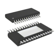
PACKAGE:
28-Pin TSSOP with Exposed Thermal Pad
(suffix LP)
Automotive
12V Power Net
Logic
Supply
ECU
The A4980 is a flexible microstepping motor driver with built-in
translator for easy operation. It is a single-chip solution, designed
to operate bipolar stepper motors in full-, half-, quarter- and
sixteenth-step modes, at up to 28 V and ±1.4 A. The A4980
can be controlled by simple Step and Direction inputs, or
through the SPI-compatible serial interface that also can be
used to program many of the integrated features and to read
diagnostic information.
The current regulator can be programmed to operate in fixed
off-time or fixed frequency PWM, with several decay modes
to reduce audible motor noise and increase step accuracy. In
addition the phase current tables can be programmed via the
serial interface to create unique microstep current profiles to
further improve motor performance for specific applications.
The current in each phase of the motor is controlled through a
DMOS full bridge, using synchronous rectification to improve
power dissipation. Internal circuits and timers prevent crossconduction and shoot-through, when switching between highside and low-side drives.
The outputs are protected from short circuits, and features
for low load current and stalled rotor detection are included.
Chip-level protection includes: hot and cold thermal warnings,
overtemperature shutdown, and overvoltage and undervoltage
lockout.
The A4980 is supplied in a 28-pin TSSOP power package with
an exposed thermal pad (package type LP). This package is
lead (Pb) free with 100% matte-tin leadframe plating.
Not to scale
Microcontroller
or
DESCRIPTION
CP1 2 VCP VBB
VDD
STEP
OAP
DIR
MS0
MS1
OAM
ENABLE
RESETn
DIAG
REF
OBP
SDI
SDO
OBM
SCK
STRn
VREG
SENSA
SENSB
OSC
AGND PGND
Stepper
Motor
Automotive
12V Power Net
Logic
Supply
Microcontroller
or
ECU
Serial Interface Control
REF
OBP
SDI
SDO
OBM
SCK
STRn
VREG
SENSA
SENSB
OSC
AGND PGND
Parallel Control
Typical Applications
A4980-DS, Rev. 4
CP1 2 VCP VBB
VDD
STEP
OAP
DIR
MS0
MS1
OAM
ENABLE
RESETn
DIAG
Stepper
Motor
�A4980
Automotive, Programmable Stepper Driver
SPECIFICATIONS
Selection Guide
Part Number
Packing*
A4980KLP-T
50 pieces per tube
A4980KLPTR-T
4000 pieces per reel
4.4 mm × 9.7 mm, 1.2 mm nominal height
TSSOP with exposed thermal pad
*Contact Allegro™ for additional packing options
Absolute Maximum Ratings With respect to GND
Characteristic
Symbol
Load Supply Voltage
VBBx
Logic Supply Voltage
VDD
Notes
Rating
Applies to VBBA and VBBB
Unit
–0.3 to 50
V
–0.3 to 6
V
–0.3 to VBB
V
–0.3 to VBB+8
V
–0.3 to 6
V
–0.3 to 8.5
V
–0.3 to 6
V
Pin OSC
–0.3 to 6
V
Pins MS0, MS1
–0.3 to 6
V
Pins SDI, SDO, SCK, STRn
–0.3 to 6
V
Pin CP1
Pins CP2, VCP
Pins STEP, DIR, ENABLE, DIAG
Pin VREG
Pin RESETn
Can be pulled to VBB with 38 kΩ
Pin REF
Pins OAP, OAM, OBP, OBM
Pins SENSA, SENSB
Ambient Operating Temperature
Range
TA
Maximum Continuous Junction
Temperature
TJ(max)
Transient Junction Temperature
TtJ
Storage Temperature Range
Tstg
Range K; limited by power dissipation
Overtemperature event not exceeding 10 s, lifetime
duration not exceeding 10 hours, guaranteed by design and
characterization
–0.3 to 6
V
–0.3 to VBB
V
–0.3 to 1
V
–40 to 150
°C
150
°C
175
°C
–55 to 150
°C
Thermal Characteristics may require derating at maximum conditions
Characteristic
Symbol
Package Thermal Resistance
(Junction to Ambient)
RθJA
Package Thermal Resistance
(Junction to Pad)
RθJP
Value
Unit
4-layer PCB based on JEDEC standard
Test Conditions*
28
ºC/W
2-layer PCB with 24.52 cm2 of copper area each side
32
ºC/W
2
ºC/W
*Additional thermal information available on the Allegro website
Allegro MicroSystems, LLC
115 Northeast Cutoff
Worcester, Massachusetts 01615-0036 U.S.A.
1.508.853.5000; www.allegromicro.com
2
�A4980
Automotive, Programmable Stepper Driver
OSC
3.3V
VREG
CP1
CP2
VDD
Oscillator
REF
RESETn
ENABLE
+
VBBA
-
OAM
SENSA
System
Control
and
Registers
Bridge
Control
Logic
Gate
Drive
DMOS Full Bridge
VBAT
VBBB
PWM
Control
OBP
OBM
REF
6-bit
DAC
DIAG
VBAT
DMOS Full Bridge
SENSA
PWM
Control
Serial Interface
SDI
SDO
SCK
STRn
VCP
OAP
Translator
MS1
MS0
Charge
Pump
REF
DAC
6-bit
DAC
STEP
DIR
Regulator
+
SENSB
SENSB
Undervoltage, Overvoltage
Cold Warning, Hot Warning, Overtemperature
Short Detect, Open Load Detect
Stall Detect
AGND
PAD
PGND
Functional Block Diagram
Allegro MicroSystems, LLC
115 Northeast Cutoff
Worcester, Massachusetts 01615-0036 U.S.A.
1.508.853.5000; www.allegromicro.com
3
�A4980
Automotive, Programmable Stepper Driver
Pin-out Diagram and Terminal List Table
SENSA
1
28
VBBA
STRn
2
27
RESETn
ENABLE
25
OAM
OSC
5
24
CP 2
23
CP1
22
VCP
21
PGND
20
VREG
SDI
6
AGND
7
Ref
Charge
Pump
26
4
I/O & Control
3
Timer
DIR
OAP
REF
8
SCK
9
VDD
10 VDD
19
STEP
OBP
11
18
OBM
MS1
12
17
SDO
MS0
13
16
DIAG
SENSB
14
15
VBBB
Reg
Pin-out Diagram
Terminal List Table
Name
Number
Description
AGND
7
Analog reference ground
CP2
24
Name
Number
PGND
21
Power Ground
Description
Charge pump capacitor terminal
REF
8
Reference input voltage
RESETn
27
Chip reset
SCK
9
Serial data clock
CP1
23
Charge pump capacitor terminal
DIAG
16
Diagnostic output
DIR
3
Direction select input
SDI
6
Serial data input
ENABLE
26
Bridge enable input
SDO
17
Serial data output
MS0
13
Microstep select input
SENSA
1
Current sense node – bridge A
MS1
12
Microstep select input
SENSB
14
Current sense node – bridge B
OAM
25
Bridge A negative output
STEP
19
Step input
OAP
4
Bridge A positive output
STRn
2
Serial data strobe
OBM
18
Bridge B negative output
VBBA
28
Motor supply – bridge A
OBP
11
Bridge B positive output
VBBB
15
Motor supply – bridge B
OSC
5
Oscillator input
VCP
22
Above supply voltage
PAD
–
Connect exposed tab to ground
VDD
10
Logic Supply
VREG
20
Regulated voltage
Allegro MicroSystems, LLC
115 Northeast Cutoff
Worcester, Massachusetts 01615-0036 U.S.A.
1.508.853.5000; www.allegromicro.com
4
�A4980
Automotive, Programmable Stepper Driver
ELECTRICAL CHARACTERISTICS1,2: valid at TJ = –40°C to 150°C, VBB = 6 to 28 V, VDD = 3 to 5.5 V; unless otherwise noted
Characteristics
Symbol
Test Conditions
Min.
Typ.
Max.
Unit
Supplies
Load Supply Voltage Range3
VBB
Load Supply Quiescent Current
IBBQ
Logic Supply Voltage Range
VDD
Logic Supply Quiescent Current
Charge Pump Voltage
Internal Regulator Voltage
Internal Regulator Dropout Voltage
Functional
0
–
50
V
3.3
–
VBBOV
V
ENABLE = 0
–
–
4
mA
Sleep mode
–
1
10
µA
Outputs Driving
3
–
5.5
V
ENABLE = 0
–
–
5
mA
ENABLE=0, VDD > 5 V
–
–
5.5
mA
Sleep mode
–
4
15
µA
VCP
With repect to VBB, VBB >7.5 V, ENABLE = 0,
RESETn = 1
–
6.7
–
V
VREG
ENABLE = 0, RESETn = 1, VBB > 7.5 V
–
7.2
–
V
VREGDO
ENABLE = 0, RESETn = 1, VBB > 3.5 V
–
100
200
mV
VBB = 13.5 V, IOUT = –1 A, TJ = 25°C
–
500
600
mΩ
VBB = 13.5 V, IOUT = –1 A, TJ = 150°C
–
900
1100
mΩ
VBB = 7 V, IOUT = –1 A, TJ = 25°C
–
625
750
mΩ
IF = 1 A
–
–
1.4
V
VBB = 13.5 V, IOUT = 1 A, TJ = 25°C
–
500
600
mΩ
VBB = 13.5 V, IOUT = 1 A, TJ = 150°C
–
900
1100
mΩ
VBB = 7 V, IOUT = 1 A, TJ = 25°C
–
625
750
mΩ
IF = –1 A
–
–
1.4
V
ENABLE = 0, RESETn = 1, VO = VBB
–120
–65
–
µA
ENABLE = 0, RESETn = 1, VO = 0 V
–200
–120
–
µA
ENABLE = 0, RESETn = 0, VO = VBB
–