A4985
DMOS Microstepping Driver with Translator
and Overcurrent Protection
FEATURES AND BENEFITS
▪
▪
▪
▪
▪
▪
▪
▪
▪
▪
▪
▪
▪
Low RDS(ON) outputs
Automatic current decay mode detection/selection
Mixed and Slow current decay modes
Synchronous rectification for low power dissipation
Internal UVLO
Crossover-current protection
3.3 and 5 V compatible logic supply
Thin profile QFN and TSSOP packages
Thermal shutdown circuitry
Short-to-ground protection
Shorted load protection
Low current Sleep mode, < 10 µA
No smoke no fire (NSNF) compliance (ET package)
PACKAGES:
The A4985 is a complete microstepping motor driver with
built-in translator for easy operation. It is designed to operate
bipolar stepper motors in full-, half-, quarter-, and eighth-step
modes. Step modes are selectable by MSx logic inputs. It has
an output drive capacity of up to 35 V and ±1 A. The A4985
includes a fixed off-time current regulator which has the ability
to operate in Slow or Mixed decay modes.
The ET package meets customer requirements for no smoke
no fire (NSNF) designs by adding no-connect pins between
critical output, sense, and supply pins. So, in the case of a
pin-to-adjacent-pin short, the device does not cause smoke
or fire. Additionally, the device does not cause smoke or fire
when any pin is shorted to ground or left open.
The translator is the key to the easy implementation of the
A4985. Simply inputting one pulse on the STEP input drives
the motor one microstep. There are no phase sequence tables,
high frequency control lines, or complex interfaces to program.
The A4985 interface is an ideal fit for applications where a
complex microprocessor is unavailable or is overburdened.
24-contact QFN
with exposed thermal pad
4 mm × 4 mm × 0.75 mm
(ES package)
During stepping operation, the chopping control in the A4985
automatically selects the current decay mode, Slow or Mixed.
In Mixed decay mode, the device is set initially to a fast decay
for a proportion of the fixed off-time, then to a slow decay for
the remainder of the off-time. Mixed decay current control
results in reduced audible motor noise, increased step accuracy,
and reduced power dissipation.
32-contact QFN
with exposed thermal pad
5 mm × 5 mm × 0.90 mm
(ET package)
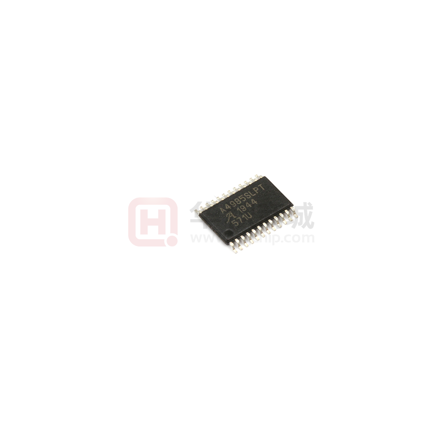
24-pin TSSOP
with exposed thermal pad
(LP Package)
DESCRIPTION
Continued on the next page…
Not to scale
Typical Application Diagram
VDD
0.1 µF
VREG ROSC
0.22 µF
0.1 µF
0.22 µF
CP1
CP2
VCP
VDD
VBB2
5 kΩ
Microcontroller or
Controller Logic
SLEEP
STEP
VBB1
100 µF
OUT1A
A4985
OUT1B
SENSE1
MS1
MS2
DIR
OUT2A
ENABLE
OUT2B
RESET
SENSE2
VREF
GND
4985-DS, Rev. 7
MCO-0000443
GND
May 28, 2019
�DMOS Microstepping Driver with Translator
and Overcurrent Protection
A4985
DESCRIPTION (continued)
Internal synchronous rectification control circuitry is provided
to improve power dissipation during PWM operation. Internal
circuit protection includes: thermal shutdown with hysteresis,
undervoltage lockout (UVLO), and crossover-current protection.
Special power-on sequencing is not required.
The A4985 is supplied in three surface mount packages: two QFN
packages, the 4 mm × 4 mm, 0.75 mm nominal overall height ES
package, and the 5 mm × 5 mm × 0.90 mm ET package. The LP
package is a 24-pin TSSOP. All three packages have exposed pads
for enhanced thermal dissipation, and are lead (Pb) free (suffix –T),
with 100% matte-tin-plated leadframes.
SELECTION GUIDE
Part Number
Package
Packing
A4985SESTR-T
24-contact QFN with exposed thermal pad
1500 pieces per 7-in. reel
A4985SETTR-T
32-contact QFN with exposed thermal pad
1500 pieces per 7-in. reel
A4985SLPTR-T
24-pin TSSOP with exposed thermal pad
4000 pieces per 13-in. reel
ABSOLUTE MAXIMUM RATINGS
Characteristic
Symbol
Load Supply Voltage
VBB
Notes
Rating
Units
35
V
Output Current
IOUT
±1
A
Logic Input Voltage
VIN
–0.3 to 5.5
V
Logic Supply Voltage
VDD
–0.3 to 5.5
V
–2.0 to 37
V
VSENSE
–0.5 to 0.5
V
VREF
5.5
V
Motor Outputs Voltage
Sense Voltage
Reference Voltage
Operating Ambient Temperature
Maximum Junction
Storage Temperature
TA
–20 to 85
°C
TJ(max)
Range S
150
°C
Tstg
–55 to 150
°C
Allegro MicroSystems
955 Perimeter Road
Manchester, NH 03103-3353 U.S.A.
www.allegromicro.com
2
�DMOS Microstepping Driver with Translator
and Overcurrent Protection
A4985
Functional Block Diagram
0.1 µF
0.22 µF
VREG
VDD
Current
Regulator
ROSC
CP1
CP2
Charge
Pump
OSC
VCP
0.1 µF
DMOS Full Bridge
REF
DAC
VBB1
OUT1A
OUT1B
PWM Latch
Blanking
Mixed Decay
STEP
Gate
Drive
DIR
RESET
OCP
Translator
MS1
Control
Logic
PWM Latch
Blanking
Mixed Decay
ENABLE
SLEEP
DAC
DMOS Full Bridge
VBB2
RS1
OUT2A
OCP
MS2
SENSE1
OUT2B
SENSE2
RS2
VREF
Allegro MicroSystems
955 Perimeter Road
Manchester, NH 03103-3353 U.S.A.
www.allegromicro.com
3
�DMOS Microstepping Driver with Translator
and Overcurrent Protection
A4985
ELECTRICAL CHARACTERISTICS [1]: at TA = 25°C, VBB = 35 V (unless otherwise noted)
Characteristics
Symbol
Test Conditions
Min.
Typ. [2]
Max.
Units
8
–
35
V
0
–
35
V
3.0
–
5.5
V
OUTPUT DRIVERS
Load Supply Voltage Range
VBB
Logic Supply Voltage Range
VDD
Output On Resistance
RDS(ON)
Body Diode Forward Voltage
VF
Motor Supply Current
IBB
Logic Supply Current
Operating
During Sleep Mode
Operating
Source Driver, IOUT = –800 mA
–
700
900
mΩ
Sink Driver, IOUT = 800 mA
–
700
900
mΩ
Source Diode, IF = –800 mA
–
–
1.3
V
Sink Diode, IF = 800 mA
–
–
1.3
V
fPWM < 50 kHz
–
–
4
mA
Operating, outputs disabled
–
–
2
mA
Sleep Mode
–
–
10
μA
fPWM < 50 kHz
–
–
8
mA
Outputs off
–
–
5
mA
Sleep Mode
–
–
10
μA
VIN(1)
VDD×0.7
–
–
V
VIN(0)
–
–
VDD×0.3
V
IDD
CONTROL LOGIC
Logic Input Voltage
Logic Input Current
Microstep Select
Logic Input Hysteresis
Blank Time
IIN(1)
VIN = VDD × 0.7
–20
很抱歉,暂时无法提供与“A4985SLPTR-T”相匹配的价格&库存,您可以联系我们找货
免费人工找货- 国内价格
- 1+8.60760
- 10+7.04160
- 30+6.18840
- 国内价格
- 1+7.32600
- 100+6.10500
- 1000+5.64300
- 2000+5.37900
- 4000+5.17000
- 国内价格 香港价格
- 1+31.087701+4.02203
- 10+23.3953410+3.02682
- 25+21.4608825+2.77654
- 100+19.33942100+2.50207
- 250+18.32694250+2.37108
- 500+18.11870500+2.34414