A6810
10-Bit Serial Input Latched Source Driver
Discontinued Product
This device is no longer in production. The device should not be
purchased for new design applications. Samples are no longer available.
Date of status change: November 1, 2010
Recommended Substitutions:
For existing customer transition, and for new customers or new applications, contact Allegro Sales.
NOTE: For detailed information on purchasing options, contact your
local Allegro field applications engineer or sales representative.
Allegro MicroSystems, Inc. reserves the right to make, from time to time, revisions to the anticipated product life cycle plan
for a product to accommodate changes in production capabilities, alternative product availabilities, or market demand. The
information included herein is believed to be accurate and reliable. However, Allegro MicroSystems, Inc. assumes no responsibility for its use; nor for any infringements of patents or other rights of third parties which may result from its use.
�A6810
10-Bit Serial Input Latched Source Driver
Features and Benefits
Description
▪ Controlled output slew rate
▪ High-speed data storage
▪ 60 V minimum output breakdown
▪ High data-input rate
▪ PNP active pull-downs
▪ Low output-saturation voltages
▪ Low-power CMOS logic and latches
▪ Improved replacements for TL4810x, UCN5810x, and
UCQ5810x
The A6810 combines 10-bit CMOS shift registers,
accompanying data latches, and control circuitry with bipolar
sourcing outputs and PNP active pull-downs. Designed
primarily to drive vacuum-fluorescent (VF) displays, the 60 V
and –40 mA output ratings also allow this device to be used in
many other peripheral power driver applications. The A6810
features an increased data input rate (compared with the older
UCN/UCQ5810-F) and a controlled output slew rate.
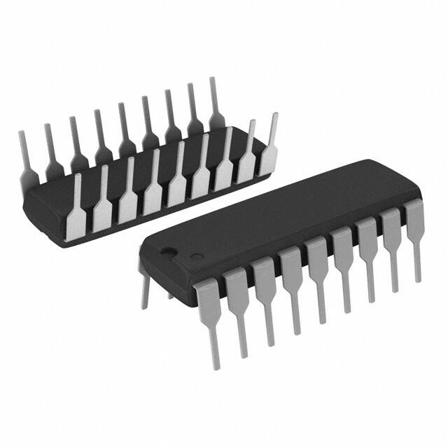
Packages:
The CMOS shift register and latches allow direct interfacing
with microprocessor-based systems. With a 3.3 or 5 V logic
supply, serial data-input rates of at least 10 MHz can be
attained
A CMOS serial data output permits cascaded connections in
applications requiring additional drive lines. Similar devices
are available as the A6812 (20-bit) and A6818 (32-bit).
18-pin DIP
(A package)
Not to scale
20-pin SOICW
(LW package)
The A6810 output source drivers are NPN Darlingtons, capable
of sourcing up to 40 mA. The controlled output slew rate reduces
electromagnetic noise, which is an important consideration in
systems that include telecommunications and microprocessors,
and to meet government emissions regulations. For inter-digit
Continued on the next page…
Functional Block Diagram
26182.124I
�10-Bit Serial Input Latched Source Driver
A6810
Description (continued)
blanking, all output drivers can be disabled and all sink drivers
turned on with a BLANKING input high. The PNP active pulldowns can sink at least 2.5 mA.
The A6810 is available in three temperature ranges for optimum
performance in commercial (S), industrial (E), and automotive (K)
applications. It is provided in two package styles, through-hole
DIP (package A) and surface-mount SOIC (package LW). Copper
leadframes, low logic-power dissipation, and low output-saturation
voltages allow all devices to source 25 mA from all outputs
continuously over the full operating temperature range.
The lead (Pb) free versions have 100% matte tin leadframe
plating.
Selection Guide
Pb-free
Packing
Ambient Temperature, TA (°C)
A6810EA-T
Part Number
Yes
21 pieces/tube
–40 to 85
A6810SA-T
Yes
21 pieces/tube
–20 to 85
A6810ELWTR-T
Yes
1000 pieces/13-in. reel
–40 to 85
A6810KLWTR-T
Yes
1000 pieces/13-in. reel
–40 to 125
Package
18-pin DIP
20-pin SOIC-W
A6810SLWTR-T
Yes
1000 pieces/13-in. reel
–20 to 85
*Variant is in production but has been determined to be LAST TIME BUY. This classification indicates that the variant is obsolete and
notice has been given. Sale of the variant is currently restricted to existing customer applications. The variant should not be purchased
for new design applications because of obsolescence in the near future. Samples are no longer available. Status date change May 3,
2010. Deadline for receipt of LAST TIME BUY orders is October 29, 2010.
Absolute Maximum Ratings*
Characteristic
Symbol
Notes
Rating
Units
Logic Supply Voltage
VDD
7.0
V
Driver Supply Voltage
VBB
60
V
Input Voltage Range
VIN
–0.3 to VDD + 0.3
V
Continuous Output Current Range
IOUT
–40 to 15
mA
Operating Ambient Temperature
Maximum Junction Temperature
Storage Temperature
Range E
–40 to 85
ºC
Range K
–40 to 125
ºC
Range S
–20 to 85
ºC
TJ(max)
150
ºC
Tstg
–55 to 125
ºC
TA
*Caution: These CMOS devices have input static protection (Class 2) but are still susceptible to damage if exposed to extremely high
static electrical charges.
Allegro MicroSystems, Inc.
115 Northeast Cutoff
Worcester, Massachusetts 01615-0036 U.S.A.
1.508.853.5000; www.allegromicro.com
2
�A6810
10-Bit Serial Input Latched Source Driver
Pin-out Diagrams
Thermal Characteristics
Characteristic
Package Thermal Resistance
Symbol
RθJA
Test Conditions*
Value Units
Package A, 1-layer PCB with copper limited to solder pads
65
ºC/W
Package LW, 1-layer PCB with copper limited to solder pads
90
ºC/W
*Additional thermal information available on the Allegro website.
Allegro MicroSystems, Inc.
115 Northeast Cutoff
Worcester, Massachusetts 01615-0036 U.S.A.
1.508.853.5000; www.allegromicro.com
3
�A6810
10-Bit Serial Input Latched Source Driver
ELECTRICAL CHARACTERISTICS at TA = +25°C (A6810S-) or over operating temperature range (A6810E-),
VBB = 60 V, logic supply operating voltage VDD = 3.0 to 5.5 V; unless otherwise noted
Characteristic
Output Leakage Current
Output Voltage
Symbol
ICEX
Test Conditions
VOUT = 0 V
Limits @ VDD = 3.3 V
Limits @ VDD = 5 V
Mln.
Typ.
Max.
Min.
Typ.
Max.
Units
—
很抱歉,暂时无法提供与“A6810EA-T”相匹配的价格&库存,您可以联系我们找货
免费人工找货