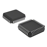
A6818
DABiC-IV 32-Bit Serial Input
Latched Source Driver
Features and Benefits
Description
▪ Controlled output slew rate
▪ 60 V minimum output break down
▪ PNP active pull-downs
▪ Low-power CMOS logic and latches
▪ High-speed data storage
▪ High data-input rate
▪ Low output-saturation voltages
▪ Improved replacements for SN75518N, SN75518NF,
UCN5818x, and UCQ5818x
The A6818 device combines a 32-bit CMOS shift register,
accompanying data latches and control circuitry, with bipolar
sourcing outputs and PNP active pull-downs. Designed
primarily to drive vacuum-fluorescent displays, the 60 V and
–40 mA output ratings also allow this device to be used in
many other peripheral power driver applications. The A6818
features an increased data-input rate (compared with the older
UCN/UCQ5818x) and a controlled output slew rate.
Package: 44 pin PLCC (suffix EP)
The CMOS shift register and latches allow direct interfacing
with microprocessor-based systems. With a 3.3 or 5 V logic
supply, typical serial data-input rates are up to 33 MHz.
A CMOS serial data output permits cascaded connections in
applications requiring additional drive lines. Similar devices
are available as the A6810 (10-bit) and A6812 (20-bit).
The A6818 output source drivers are NPN Darlingtons,
capable of sourcing up to 40 mA. The controlled output slew
rate reduces electromagnetic noise, which is an important
consideration in systems that include telecommunications
and/or microprocessors and to meet government emissions
Not to scale
Continued on the next page…
Functional Block Diagram
V DD
CLOCK
SERIAL
DATA IN
SERIAL-PARALLEL SHIFT REGISTER
STROBE
LATCHES
LOGIC
SUPPLY
SERIAL
DATA OUT
BLANKING
MOS
BIPOLAR
VBB
GROUND
26182.128F
OUT 1 OUT 2 OUT 3
OUT N
LOAD
SUPPLY
Dwg. FP-013-1
�DABiC-IV 32-Bit Serial Input
Latched Source Driver
A6818
Description (continued)
regulations. For inter-digit blanking, all output drivers can be
disabled and all sink drivers turned on with a BLANKING input
high. The PNP active pull-downs will sink at least 2.5 mA.
Three temperature ranges are available for optimum performance
in commercial (suffix S-), industrial (E-), and extended industrial
(K-) applications. The package style provided is the minimum-area
surface-mount PLCC (suffix -EP). Copper lead frames, low logic-
power dissipation, and low output-saturation voltages allow these
devices to drive most multiplexed vacuum-fluorescent displays
over the maximum operating temperature range.
The lead (Pb) free versions have 100% matte tin leadframe
plating.
Selection Guide
Part Number
Pb-free
Packing
Ambient Temperature
TA (°C)
Yes
450 pieces/13-in. reel
–40 to 85
–
450 pieces/13-in. reel
–40 to 125
Yes
450 pieces/13-in. reel
–20 to 85
A6818EEPTR-T
A6818KEPTR
A6818SEPTR-T
Absolute Maximum Ratings*
Characteristic
Symbol
Logic Supply Voltage
VDD
Notes
Rating
Units
7.0
V
Driver Supply Voltage
VBB
60
V
Input Voltage Range
VIN
–0.3 to VDD + 0.3
V
Continuous Output Current Range
IOUT
Operating Ambient Temperature
Maximum Junction Temperature
Storage Temperature
–40 to 15
mA
Range E
–40 to 85
ºC
Range K
–40 to 125
ºC
Range S
–20 to 85
ºC
TJ(max)
150
ºC
Tstg
–55 to 125
ºC
TA
*Caution: These CMOS devices have input static protection (Class 2) but are still susceptible to damage if exposed to extremely high
static electrical charges.
Allegro MicroSystems, Inc.
115 Northeast Cutoff
Worcester, Massachusetts 01615-0036 U.S.A.
1.508.853.5000; www.allegromicro.com
2
�DABiC-IV 32-Bit Serial Input
Latched Source Driver
A6818
Pin-out Diagram
Thermal Characteristics
Characteristic
Package Thermal Resistance
Symbol
Test Conditions*
RθJA
Value Units
1-layer PCB with copper limited to solder pads
54
ºC/W
*Additional thermal information available on the Allegro website.
ALLOWABLE PACKAGE POWER
DISSIPATION IN WATTS
3.0
2.5
2.0
1.5
1.0
SUFFIX 'EP', RQJA = 54oC/W
0.5
0
25
TYPICAL INPUT CIRCUIT
50
75
100
125
AMBIENT TEMPERATURE IN oC
150
TYPICAL OUTPUT DRIVER
Allegro MicroSystems, Inc.
115 Northeast Cutoff
Worcester, Massachusetts 01615-0036 U.S.A.
1.508.853.5000; www.allegromicro.com
3
�DABiC-IV 32-Bit Serial Input
Latched Source Driver
A6818
TRUTH TABLE
Serial
Shift Register Contents
Data Clock
Input Input I1 I2 I3 ... IN-1 IN
Serial
Data Strobe
Output Input
Latch Contents
I1
I2
I3
...
IN-1
Output Contents
IN Blanklng
I1 I2 I3 ... IN-1 IN
H
H
R1 R2 ...
RN-2 RN-1
RN-1
L
L
R1 R2 ...
RN-2 RN-1
RN-1
X
R1 R2 R3 ...
RN-1 RN
RN
X
X
X
L
R1 R2 R3 ...
RN-1 RN
PN
H
P1 P2 P3 ...
PN-1 PN
L
P1 P2 P3 ... PN-1 PN
X
X
H
L
X
X
...
P1 P2 P3 ...
X
PN-1 PN
X
X
...
X
L
L
... L
L
L = Low Logic Level H = High Logic Level X = Irrelevant P = Present State R = Previous State
Allegro MicroSystems, Inc.
115 Northeast Cutoff
Worcester, Massachusetts 01615-0036 U.S.A.
1.508.853.5000; www.allegromicro.com
4
�DABiC-IV 32-Bit Serial Input
Latched Source Driver
A6818
ELECTRICAL CHARACTERISTICS at TA = +25°C (A6818S-) or over operating temperature range (A6818Eand A6818K-), VBB = 60 V, unless otherwise noted
Characteristic
Output Leakage Current
Output Voltage
Symbol
ICEX
Test Conditions
VOUT = 0 V
Limits @ VDD = 3.3 V
Limits @ VDD = 5 V
Mln.
Typ.
Max.
Min.
Typ.
Max.
Units
—
很抱歉,暂时无法提供与“A6818SEP-T”相匹配的价格&库存,您可以联系我们找货
免费人工找货