A8436 Photoflash Capacitor Charger with IGBT Driver
Features and Benefits
▪ ▪ ▪ ▪ ▪ ▪ ▪ ▪ ▪ Power with 1 Li+ or 2 Alkaline/NiMH/NiCAD batteries Adjustable output voltage >75% efficiency Three levels of switch current limit: 1.0, 1.2, 1.4 A Fast charge time Charge complete indication Integrated IGBT driver with trigger No primary-side Schottky diode needed Low-profile package (0.75 mm nominal height)
Description
The A8436 is a highly integrated IC that charges photoflash capacitors for digital and film cameras. It also features an integrated IGBT driver that facilitates the flash discharge function and saves board space. To charge the photoflash capacitor, the A8436 integrates a 40 V, DMOS switch that drives the transformer in a flyback topology, allowing optimized design with tight coupling and high efficiency. A proprietary control scheme optimizes the capacitor charging time. Low quiescent current and low shutdown current further improve system efficiency and extend battery life. Three levels of switch current limit are provided: 1.0, 1.2, and 1.4 A. The level is determined by configuring the ILIM pin as grounded, floating, or pulled up to IC supply voltage, respectively. The CHARGE pin enables the A8436 and starts the charging of the output capacitor. When the designated output voltage is reached, the A8436 stops the charging until the CHARGE pin is toggled again. Pulling the CHARGE pin low stops charging. The DONE pin is an open-drain indicator of when ¯¯¯¯ ¯ ¯ ¯¯ the designated output voltage is reached. The A8436 can be used with two Alkaline/NiMH/NiCAD or one single-cell Li+ battery connected to the transformer primary. Connect the VIN pin to a 3.0 to 5.5 V supply, which can be either the system rail or the Li+ battery, if used. The A8436 is available in a very low profile (0.75 mm) 10terminal 3×3 mm MLP/TDFN package, making it ideal for space-constrained applications. It is lead (Pb) free, with 100% matte-tin leadframe plating.
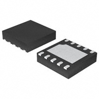
Package: 10 pin TDFN/MLP (suffix EJ)
Approximate Scale 1:1
Typical Applications
VBIAS 3.0 to 5.5 V Two Alkaline/NiMH/NiCAD or one Li+ battery or 1.5 to 5.5 V D1 VBATT VOUT T1 +
C1 0.1 μF C2 4.7 μF
One Li+ battery VBATT or 3.0 to 5.5 V
T1
D1
VOUT
R1 R2
R5
100 k 1.4 A 1.2 A (N.C.) 1.0 A
10 k
R4
COUT
R5
100 k 1.4 A 1.2 A (N.C.) 1.0 A
10 k
R4
C1 0.1 μF
C2 4.7 μF
R1 R2
COUT
VIN ILIM DONE CHARGE
SW FB
VIN ILIM DONE CHARGE
SW FB
A8436
IGBTDRV GND
R3
A8436
IGBTDRV GND
R3
R6
10 k
TRIGGER
R7
To IGBT Gate
R6
10 k
10 k
TRIGGER
R7
To IGBT Gate
10 k
Figure 1. Typical circuit with separate power supply to transformer A8436-DS, Rev. 3
Figure 2. Typical circuit with single power supply
�A8436
Description (continued) Applications include: ▪ ▪ ▪ ▪ Digital camera flash Film camera flash Cell phone flash Emergency strobe light
Photoflash Capacitor Charger with IGBT Driver
Selection Guide
10-pin TDFN/MLP *Contact Allegro for additional packing options
Part Number A8436EEJTR-T
Package
Packing*
1500 pieces/ 7-in. reel
Absolute Maximum Ratings
Characteristic SW pin IGBTDRV pin FB pin All other pins Operating Ambient Temperature Maximum Junction Temperature Storage Temperature Symbol VSW VIGBTDRV VFB VX TA TJ(max) Tstg Range E Notes Rating –0.3 to 40 –0.3 to VIN + 0.3 –0.3 to VIN –0.3 to 7 –40 to 85 150 –55 to 150 Units V V V V ºC ºC ºC
Package Thermal Characteristics
Characteristic Package Thermal Resistance Symbol RθJA Test Conditions* 4layer PCB, based on JEDEC standard Rating Units 45 ºC/W
*Additional information is available on the Allegro website.
Allegro MicroSystems, Inc. 115 Northeast Cutoff, Box 15036 Worcester, Massachusetts 01615-0036 (508) 853-5000 www.allegromicro.com
2
�A8436
Photoflash Capacitor Charger with IGBT Driver
Functional Block Diagram
SW VIN DCM Comparator CMP3
18 μs
Control Logic
1.2 V
H→L Triggered Timer
S SET Q
Q
40 V DMOS
CMP2 ILIM Comparator ILIM ILIM Decoder Adjustable Reference Enable
R
CLR Q
Q Q
SET
S R
FB CMP1
CLR
CHARGE
DONE VIN TRIGGER One-Shot
1.2 V
IGBTDRV
GND
Device Pin-out Diagram
Terminal List Table
Number 1 2 3 4 5 6 7 8 9 10 Name NC IGBTDRV VIN GND CHARGE SW TRIGGER ¯¯ ¯¯ DONE ¯ ¯ ¯¯ FB ILIM Function No connection IGBT driver gate drive output Power supply input Device ground Charging enable; set to low to power-off the A8436 Switch, internally connected to the DMOS power FET drain Strobe signal input Open drain, when pulled low by internal MOSFET, indicates that charging target level has been reached Output voltage feedback Switch current limit setting; sets three discreet levels
NC IGBTDRV VIN GND CHARGE
1 2 3 4 5
10 ILIM 9 8 7 6 FB DONE TRIGGER SW
Allegro MicroSystems, Inc. 115 Northeast Cutoff, Box 15036 Worcester, Massachusetts 01615-0036 (508) 853-5000 www.allegromicro.com
3
�A8436
Photoflash Capacitor Charger with IGBT Driver
ELECTRICAL CHARACTERISTICS Typical values at TA = 25°C and VIN = 3.3 V (unless otherwise noted)
Characteristics Supply Voltage* Supply Current Symbol VIN IIN Charging Charging done Shutdown (VCHARGE = 0 V, VTRIGGER = 0 V) VILIM < 1.0 V ILIM pin floating VILIM > VIN – 1.3 V VIN = 3.3 V, ID = 800 mA, TA = 25°C VSW = 35 V Test Conditions Min. 3 – – – – 1.08 – – – – – – 2 – – 32 μA into ¯ ¯ ¯ ¯ pin DONE ¯ ¯ ¯¯ VFB = 1.205 V VIN rising – 1.187 – 2.55 – – – – 2 – – – – – Typ. – 5 1 0.01 1.0 1.2 1.4 0.27 – 18 18 – – – – – Max. Units 5.5 – 10 1 – 1.32 – – 1 – – 1 – 0.8 1 100 V mA μA μA A A A Ω μA μs μs μA V V μA mV V nA V mV Ω Ω μA V V ns ns ns ns
Primary Side Current Limit SW On Resistance SW Leakage Current* SW Maximum Off-Time SW Maximum On-Time CHARGE Input Current CHARGE Input Voltage* ¯ ¯ ¯ ¯ Output Leakage Current* DONE ¯ ¯ ¯¯ ¯ ¯ ¯ ¯ Output Low Voltage* DONE ¯ ¯ ¯¯ FB Voltage Threshold* FB Input Current UVLO Enable Threshold UVLO Hysteresis IGBT Driver IGBTDRV On Resistance to VIN IGBTDRV On Resistance to GND TRIGGER Input Current
ISWLIM RDS(On)SW ISWLKG tOFF(Max) tON(Max) ICHARGE VCHARGE(H) VCHARGE(L) IDONELKG VDONE(L) VFB IFB VUVLO VUVLOHYS
VCHARGE = VIN
1.205 1.223 –120 – 2.65 2.75 150 – 5 6 – – – 30 30 70 70 – – 1 – 0.8 – – – –
RDS(On)I-V VIN = 3.3 V, VIGBTDRV = 1.5 V RDS(On)I-G VIN = 3.3 V, VIGBTDRV = 1.5 V ITRIGGER VTRIGGER = VIN VTRIGGER(H) TRIGGER Input Voltage* VTRIGGER(L) Propagation Delay, Rising tDr Rgate=12 Ω, CLOAD = 6500 pF, VIN = 3.3 V Propagation Delay, Falling tDf Rgate=12 Ω, CLOAD = 6500 pF, VIN = 3.3 V Output Rise Time tr Rgate=12 Ω, CLOAD = 6500 pF, VIN = 3.3 V Output Fall Time tf Rgate=12 Ω, CLOAD = 6500 pF, VIN = 3.3 V *Guaranteed by design and characterization over operating temperature range, –40°C to 85°C.
Allegro MicroSystems, Inc. 115 Northeast Cutoff, Box 15036 Worcester, Massachusetts 01615-0036 (508) 853-5000 www.allegromicro.com
4
�A8436
Photoflash Capacitor Charger with IGBT Driver
Operation Timing Diagram
VIN CHARGE SW
VUVLO
Target VOUT
VOUT DONE TRIGGER IGBTDRV A B C D E F
Explanation of Events:
A. B. C. D. E. F. Start charging by pulling CHARGE to high, provided that VIN is above the VUVLO level. Charging stops when VOUT reaches the target voltage. ¯ ¯ ¯ ¯ goes low, to signal the DONE ¯ ¯ ¯¯ completion of the charging process. Start a new charging process with a low-to-high transition at the CHARGE pin. Pull CHARGE to low, to put the controller in low-power standby mode. Charging does not start, because VIN is below VUVLO level when CHARGE goes high. After VIN goes above VUVLO, another low-to-high transition at the CHARGE pin is required to start charging.
Allegro MicroSystems, Inc. 115 Northeast Cutoff, Box 15036 Worcester, Massachusetts 01615-0036 (508) 853-5000 www.allegromicro.com
5
�A8436
Photoflash Capacitor Charger with IGBT Driver
Tests performed using application circuit shown in figure 6 (unless otherwise noted)
Performance Characteristics
Charging Waveforms
VOUT
Symbol C1 C4 t Conditions
Parameter VOUT IBATT(Avg) time Parameter VBATT VBIAS COUT
Units/Division 50 V 200 mA 1s Value 2.5 V 3.3 V 100 μF
IBATT C4
C1
t
VOUT
Symbol C1 C4 t Conditions
Parameter VOUT IBATT(Avg) time Parameter VBATT VBIAS COUT
Units/Division 50 V 200 mA 1s Value 3.6 V 3.3 V 100 μF
IBATT C4
C1
t
VOUT
Symbol C1 C4 t Conditions
Parameter VOUT IBATT(Avg) time Parameter VBATT VBIAS COUT
Units/Division 50 V 200 mA 1s Value 4.2 V 3.3 V 100 μF
IBATT C4
C1
t
Allegro MicroSystems, Inc. 115 Northeast Cutoff, Box 15036 Worcester, Massachusetts 01615-0036 (508) 853-5000 www.allegromicro.com
6
�A8436
Performance Characteristics, continued
Photoflash Capacitor Charger with IGBT Driver
Tests performed using application circuit shown in figure 6 (unless otherwise noted)
Charge Time
VBIAS = 3.3 V, COUT = 100 μF Connect VBATT to a separate power supply
88 77 90 80
Efficiency
VBATT = VBIAS , TA = 25°C
Charge Time (s)
Charge Time (s)
66 55 44 33 22 2.0 2
Efficiency (%)
70 60 50 40 100
VBATT = 5.0 V VBATT = 4.2 V VBATT = 3.0 V
VV ==3320VV 20 OUT OUT VV ==3300VV 00 OUT OUT
2.5 2.5
33.0 3.53.5 4 4.0 4.5 4.5 5 VBATT (V)V) VBATT (
5.0 5.5
5.5 6
6.0
150
200 VOUT (V)
250
300
350
Typical Switching Waveform
VBATT C3 VOUT
Symbol C1 C2 C3 C4 t Conditions
Parameter VOUT VSW VBATT IPrimary time Parameter VOUT VBATT
Units/Division 50 V 10 V 5V 500 mA 2 μs Value 300 V VIN
C2
VSW
IPrimary
C4 C1
t
IGBT Drive Timing Definition
TRIGGER
50%
50%
t Dr
tr
90%
t Df
tf
90% 10%
IGBTDRV
10%
Allegro MicroSystems, Inc. 115 Northeast Cutoff, Box 15036 Worcester, Massachusetts 01615-0036 (508) 853-5000 www.allegromicro.com
7
�A8436
Photoflash Capacitor Charger with IGBT Driver
Performance Characteristics, continued
IGBT Drive waveforms are measured with R-C load (12 Ω, 6800 pF)
IGBT Drive Performance Rising Signal
tr VIGBTDRV
Symbol C2 C3 t Conditions
Parameter VIGBTDRV VTRIGGER time Parameter tDr tr CLOAD Rgate
Units/Division 1V 1V 50 ns Value 22.881 ns 63.125 ns 6800 pF 12 Ω
C2 VTRIGGER
C3
t
Falling Signal
tf
Symbol C2 C3 t Conditions
Parameter VIGBTDRV VTRIGGER time Parameter tDf tf CLOAD Rgate
Units/Division 1V 1V 50 ns Value 27.427 ns 65.529 ns 6800 pF 12 Ω
C2
VIGBTDRV
C3
VTRIGGER t
Allegro MicroSystems, Inc. 115 Northeast Cutoff, Box 15036 Worcester, Massachusetts 01615-0036 (508) 853-5000 www.allegromicro.com
8
�A8436
Photoflash Capacitor Charger with IGBT Driver
Functional Description
Overview The A8436 is a photoflash capacitor charger control IC with adjustable input current limiting. It also integrates an IGBT driver for strobe operation of the flash tube, dramatically saving board space in comparison to discrete solutions for strobe flash operation. The control logic is shown in the functional block diagram. The charging operation of the A8436 is started by a low-to-high signal on the CHARGE pin, provided that VIN is above VUVLO level. If CHARGE is already high before VIN reaches VUVLO , another low-to-high transition on the CHARGE pin is required to start the charging. When a charging cycle is initiated, the transformer primary side current, IPrimary, ramps up linearly at a rate determined by the combined effect of the battery voltage, VBATT , and the primary side inductance, LPrimary. When IPrimary reaches the current limit, ISWLIM , set by configuring the ILIM pin, the internal MOSFET is turned off immediately, allowing the energy to be pushed into the photoflash capacitor, COUT, from the secondary winding. The secondary side current drops linearly as COUT charges. While the internal MOSFET switch is turned off, the output voltage, VOUT, is sensed by a resistor string, R1 through R3, connected between the anode of the output diode, D1, and ground. This resistor string forms a voltage divider that feeds back to the FB pin. The resistors must be sized to achieve a desired output voltage level based on a typical value of 1.205 V at the FB pin. As soon as VOUT reaches the desired value, the charging process is terminated. The user may toggle the CHARGE pin to refresh the photoflash capacitor. Switch On-Time and Off-Time Control The A8436 implements an adaptive on-time/off-time control. (For circuit details, please refer to the the Control Logic block in the simplified Functional Block Diagram on page 2.) On-time duration, tON , is determined by input voltage, VIN, transformer primary inductance, LPrimary, and the set current limit, ISWLIM . Off-time duration, tOFF , depends on the operating conditions during switch off-time. The A8436 applies its two charging modes, Fast Charging mode and Timer mode, according to those conditions.
Fast Charging and Timer Modes The IC operates in the Fast Charging mode when the photoflash capacitor, COUT, is only partially discharged. In Fast Charging mode, the converter operates near the discontinuous boundary, and a sensing circuit tracks the fly-back voltage at the SW node. As soon as this voltage swings below 1.2 V, the internal MOSFET switch is turned on again, starting the next charging cycle. The IC operates in the Timer mode when beginning to charge a completely discharged photoflash capacitor, usually when the output voltage, VOUT, is less than approximately 10 to 20 V. Timer mode is a fixed 18 μs off-time control. One advantage of the A8436 watchdog timer control scheme is that it limits the initial current surge and thus acts as a “soft-start.” As shown in figure 3, the timer mode only lasts a small fraction of a second (usually < 100 ms). It can be recognized by its lower initial input charging current as a result of a lower duty cycle. As output voltage rises to more than 10 to 20 V, the adaptive Fast Charging mode takes over the control, raising the average input current level.
Timer Mode
Fast Charging Mode
IBATT(Avg)
VOUT
Figure 3. Sequencing of Timer mode and Fast Charging mode (time axis scale is 1 s per division)
Allegro MicroSystems, Inc. 115 Northeast Cutoff, Box 15036 Worcester, Massachusetts 01615-0036 (508) 853-5000 www.allegromicro.com
9
�A8436
Photoflash Capacitor Charger with IGBT Driver
Charging Cycles for a Completely Discharged Photoflash Capacitor
VBATT C3
Figure 4A. Initial two cyles of charging a completely discharged photoflash capacitor. In these two cycles, off-time (VSW low) is controlled by the internal 18 μs timer (Timer mode). Note that, in the first cycle, IPrimary starts near 0 A, but in the second cycle, it starts at a higher level. This indicates that the transformer core did not reset during the first cycle.
VSW C2
C4 C1
IPrimary VOUT
t
VBATT C3
VSW
Figure 4B. During the intermediate cycles, the output voltage, VOUT, has increased. ISecondary goes discontinuous, leading to the ringing of VSW . The amplitude of the ringing is not great enough, however, to pull VSW below 1.2 V, so the A8436 remains in Timer mode.
C2
C4 C1
IPrimary VOUT
t
VBATT C3
VSW
Figure 4C. The final cycle of Timer mode is shown, followed by a series of cycles in Fast Charging mode. VSW is able to ring down below 1.2 V in every cycle as a result of increased VOUT , triggering the turn-on of the main MOSFET switch.
Symbol C1 C2 C3 C4 t Conditions Parameter VOUT VSW VBATT IPrimary time Parameter VBATT Units/Division 50 V 10 V 5V 500 mA 5 μs Value VIN
C2
C4 C1
IPrimary VOUT
t
Allegro MicroSystems, Inc. 115 Northeast Cutoff, Box 15036 Worcester, Massachusetts 01615-0036 (508) 853-5000 www.allegromicro.com
10
�A8436
Photoflash Capacitor Charger with IGBT Driver
To understand the Timer mode, it is noted that the secondary winding charge current, ISecondary, decreases linearly at a rate of:
dISecondary
where:
dt
=
VOUT
Lower input current offers the advantage of a longer battery lifetime. For faster charging time, however, use the highest current limit. ISWLIM may be adjusted during charging. Figure 5 shows a waveform of ISWLIM being adjusted during charging. ISWLIM is lowered from 1.4 to 1.2 A, and charging slows slightly at the lower current level.
LPrimary
N2
(1)
ISecondary is the secondary side current, LPrimary is the primary side inductance, and N is the transformer turns ratio (NSecondary / NPrimary). As shown in the three panels of figure 4, when the A8436 charges a fully-discharged photoflash capacitor, ISecondary decreases very slowly due to the low initial VOUT. The A8436 internal timer (Timer mode) sets a maximum timeframe of 18 μs for the offtime as long as the SW node voltage is greater than 1.2 V. When the off-time passes 18 μs, the internal MOSFET switch is turned on, initiating the next charging cycle .
ISWLIM = 1.4 A ISWLIM = 1.2 A
IIN(Avg)
Input Current Limiting The peak input current, ISWLIM , can be set to three levels by configuring the ILIM pin:
ISWLIM Setting (A) 1.0 1.2 1.4 Float Pull up to IC supply voltage with a 1 to 10 kΩ resistor
Figure 5. Reducing ISWLIM during charging
VOUT
ILIM Pin Connection External ground
Allegro MicroSystems, Inc. 115 Northeast Cutoff, Box 15036 Worcester, Massachusetts 01615-0036 (508) 853-5000 www.allegromicro.com
11
�A8436
Photoflash Capacitor Charger with IGBT Driver
Applications Information
Transformer Design
Turns Ratio. The minimum transformer turns ratio, N,
LPrimary (μH), use the following formula:
(Secondary:Primary) should be chosen based on the following formula:
LPrimary ≥
300 × 10−9 × VOUT N × ISWLIM
.
(3)
N≥
where: VOUT (V) is the required output voltage level, VD_Drop (V) is the forward voltage drop of the output diode(s), VBATT (V) is the transformer battery supply, and 40 (V) is the rated voltage for the internal MOSFET switch, representing the maximum allowable reflected voltage from the output to the SW pin. For example, if VBATT is 3.5 V and VD_Drop is 1.7 V (which could be the case when two high voltage diodes were in series), and the desired VOUT is 320 V, then the turns ratio should be at least 8.9. In a worst case, when VBATT is highest and VD_Drop and VOUT are at their maximum tolerance limit, N will be higher. Taking VBATT = 5.5 V, VD_Drop = 2 V, and VOUT = 320 V × 102 % = 326.4 V as the worst case condition, N can be determined to be 9.5. In practice, always choose a turns ratio that is higher than the calculated value to give some safety margin. In the worst case example, a minimum turns ratio of N = 10 is recommended.
Primary Inductance. The A8436 has a minimum switch off-time,
VOUT + VD_Drop 40 − VBATT
(2)
Ideally, the charging time is not affected by transformer primary inductance. In practice, however, it is recommended that a primary inductance be chosen between 10 μH and 20 μH. When LPrimary is much lower than 10 μH, the converter operates at higher frequency, which increases switching loss proportionally. This leads to lower efficiency and longer charging time. When LPrimary is greater than 20 μH, the rating of the transformer must be dramatically increased to handle the required power density, and the series resistances are usually higher. A design that is optimized to achieve a small footprint solution would have an LPrimary of 12 to 14 μH, with minimized leakage inductance and secondary capacitance, and minimized primary and secondary series resistance. Please refer to the table Recommended Components for more information.
Leakage Inductance and Secondary Capacitance. The trans-
tOFF(min) , of 300 ns, to ensure correct SW node voltage sensing. As a loose guideline when choosing the primary inductance,
former design should minimize the leakage inductance to ensure the turn-off voltage spike at the SW node does not exceed the 40 V limit. An achievable minimum leakage inductance for this application, however, is usually compromised by an increase in parasitic capacitance. Furthermore, the transformer secondary capacitance should be minimized. Any secondary capacitance is multiplied by N2 when reflected to the primary, leading to high initial current swings when the switch turns on, and to reduced efficiency.
VBIAS 3.0 to 5.5 V
Two Alkaline/NiMH/NiCAD or one Li + VBATT 1.5 to 5.5 V D1 T1 +
C1 0.1 μF C2 4.7 μF
VOUT
Symbol
C1 C2 D1 T1
Rating
0.1 μF, X5R or X7R, 10 V 4.7 μF, X5R or X7R, 10 V Fairchild Semiconductor BAV23S (dual diode connected in series) Tokyo Coil Engineering T-16-024A, LPrimary = 12 μH, N = 10.2 1206 resistors, 1 % 0603 resistor, 1 % Pull-up resistors Pull-down resistors
R5
100 k
10 k
R4
150 k
R1 R2
100 μF 330 V
COUT
VIN ILIM DONE CHARGE
SW FB
150 k
A8436
IGBTDRV GND
1.2 k
R3
R1, R2 R3 R4, R5 R6, R7
R6
10 k
TRIGGER
R7
To IGBT Gate
10 k
Figure 6. Typical circuit for photoflash application. Configured for ISWLIM of 1.4 A.
Allegro MicroSystems, Inc. 115 Northeast Cutoff, Box 15036 Worcester, Massachusetts 01615-0036 (508) 853-5000 www.allegromicro.com
12
�A8436
Adjusting Output Voltage
Photoflash Capacitor Charger with IGBT Driver
The A8436 senses output voltage during switch off-time. This allows the voltage divider network, R1 through R3 (see figure 6), to be connected at the anode of the high voltage output diode, D1, eliminating power loss due to the feedback network when charging is complete. The output voltage can be adjusted by selecting proper values of the voltage divider resistors. Use the following equation to calculate values for Rx (Ω):
internal MOSFET switch is closed, and the primary-side current starts to ramp-up. It can be calculated as:
VD_ Peak = VOUT + N × V ATT . B
(5) (6)
The peak current of the rectifying diode, ID_Peak, is calculated as :
ID_ Peak = IPrimary_Peak / N .
Input Capacitor Selection
R1 + R2 VOUT = −1 . R3 VFB
(4)
R1 and R2 together need to have a breakdown voltage of at least 300 V. A typical 1206 surface mount resistor has a 150 V breakdown voltage rating. It is recommended that R1 and R2 have similar values to ensure an even voltage stress between them. Recommended values are: R1 = R2 = 150 kΩ (1206) R3 = 1.2 kΩ (0603) which together yield a stop voltage of 303 V. Using higher resistance values for R1, R2, and R3 does not offer significant efficiency improvement, because the power loss of the feedback network occurs mainly during switch off-time, and because the off-time is only a small fraction of each charging cycle.
Output Diode Selection
Ceramic capacitors with X5R or X7R dielectrics are recommended for the input capacitor, C2. It should be rated at least 4.7 μF / 6.3 V to decouple the battery input, VBATT , at the primary of the transformer. When using a separate bias, VBIAS , for the A8436 VIN supply, connect at least a 0.1 μF / 6.3 V bypass capacitor to the VIN pin. Layout Guidelines Key to a good layout for the photoflash capacitor charger circuit is to keep the parasitics minimized on the power switch loop (transformer primary side) and the rectifier loop (secondary side). Use short, thick traces for connections to the transformer primary and SW pin. Output voltage sensing circuit elements must be kept away from switching nodes such as SW pin. Make sure that there is no GND plane underneath R1 and R2, because parasitic capacitance to ground will affect sensing accuracy. It is important that the ¯ ¯ DO ¯¯ NE ¯ ¯ signal trace be routed away from the transformer and other ¯¯ switching traces, in order to minimize noise pickup. In addition, high voltage isolation rules must be followed carefully to avoid breakdown failure of the circuit board.
Part Number GRM188R71C104KA01D LMK212BJ475KG EPH-331ELL101B131S BAV23S GSD2004S 9C12063A1503FKHFT 9T06031A1201FBHFT LDT565630T-002 T-16-024A ST-532517A SBL-5.6-1 Murata Taiyo Yuden Chemi-Con Philips Semiconductor, Fairchild Semiconductor Vishay Yageo Yageo TDK Tokyo Coil Engineering Asatech Kijima-Musen Source
Choose the rectifying diode(s), D1, to have small parasitic capacitance (short reverse recovery time) while satisfying the reverse voltage and forward current requirements. The peak reverse voltage of the diode, VD_Peak , occurs when the
Recommended Components Table Component Rating 0.1 μF, ± 10%, 16 V X7R ceramic C1 Input Capacitor capacitor (0603) 4.7 μF, ± 10%, 10 V, X5R ceramic C2 Input Capacitor capacitor (0805) COUT Photoflash Capacitor 330 V, 100 μF (or 19 to 180 μF) D1 Output Diode R1 and R2 FB Resistors R3 FB Resistors 2 x 250 V, 225 mA, 5 pF 2 x 300 V, 225 mA, 5 pF 150 kΩ, 1/4 W ± 1% (1206) 1.20 kΩ 1/10 W ± 1% (0603) 1:10.2, LPrimary = 14.5 μH 1:10.2, LPrimary = 12 μH 1:10, LPrimary = 10.8 μH 1:10.2, LPrimary = 9.8 μH
T1 Transformer
Allegro MicroSystems, Inc. 115 Northeast Cutoff, Box 15036 Worcester, Massachusetts 01615-0036 (508) 853-5000 www.allegromicro.com
13
�A8436
Photoflash Capacitor Charger with IGBT Driver
Package EJ, 10-Contact TDFN/MLP
3.15 .124 2.85 .112 Preliminary dimensions, for reference only (reference JEDEC MO-229 WEED) Dimensions in millimeters U.S. Customary dimensions (in.) in brackets, for reference only Dimensions exclusive of mold flash, gate burrs, and dambar protrusions Exact case and lead configuration at supplier discretion within limits shown A Terminal #1 mark area B Exposed thermal pad (reference dimensions only, terminal #1 identifier appearance at supplier discretion) C Reference pad layout (reference IPC7351 SON50P300X300X80-11WEED2M); adjust as necessary to meet application process requirements 10X 0.08 [.003] C 10X 0.30 .012 0.18 .007 0.10 [.004] M C A B 0.05 [.002] M C 0.50 .020 0.30 .012 NOM 8X 0.20 .008 MIN C 0.22 X 0.22 [.009 X .009] REF 1.64 .065 NOM 3.10 .122 NOM B 0.50 .020 NOM 1 2 10
A B
3.15 .124 2.85 .112 A 1 2 C
SEATING PLANE 0.80 .031 0.70 .028 0.20 .008 REF 0.05 .002 0.00 .000
1.64 .065 NOM
0.50 .020 0.30 .012
0.85 .033 NOM
10 8X 0.20 .008 MIN 2.38 .094 NOM
2.38 .094 NOM
The products described here are manufactured under one or more U.S. patents or U.S. patents pending. Allegro MicroSystems, Inc. reserves the right to make, from time to time, such departures from the detailed specifications as may be required to permit improvements in the performance, reliability, or manufacturability of its products. Before placing an order, the user is cautioned to verify that the information being relied upon is current. Allegro products are not authorized for use as critical components in life-support devices or systems without express written approval. The information included herein is believed to be accurate and reliable. However, Allegro MicroSystems, Inc. assumes no responsibility for its use; nor for any infringement of patents or other rights of third parties which may result from its use.
Copyright©2005, 2006 Allegro MicroSystems, Inc.
Allegro MicroSystems, Inc. 115 Northeast Cutoff, Box 15036 Worcester, Massachusetts 01615-0036 (508) 853-5000 www.allegromicro.com
14
�