A8439
Protected Quad Driver with Fault Detection and Sleep Mode
Discontinued Product
This device is no longer in production. The device should not be
purchased for new design applications. Samples are no longer available.
Date of status change: December 3, 2013
Recommended Substitutions:
For existing customer transition, and for new customers or new applications, contact Allegro Sales.
NOTE: For detailed information on purchasing options, contact your
local Allegro field applications engineer or sales representative.
Allegro MicroSystems, LLC reserves the right to make, from time to time, revisions to the anticipated product life cycle plan
for a product to accommodate changes in production capabilities, alternative product availabilities, or market demand. The
information included herein is believed to be accurate and reliable. However, Allegro MicroSystems, LLC assumes no responsibility for its use; nor for any infringements of patents or other rights of third parties which may result from its use.
�A8439
Photoflash Capacitor Charger
with IGBT Driver and Refresh
Features and Benefits
Description
▪
▪
▪
▪
▪
▪
▪
▪
▪
The A8439 is a highly integrated IC that charges photoflash
capacitors for digital and film cameras. An integrated MOSFET
switch drives the transformer in a flyback topology. It also
features an integrated IGBT driver that facilitates the flash
discharge function and saves board space.
Power with 1 Li+ or 2 Alkaline/NiMH/NiCAD batteries
Adjustable output voltage
Auto-refresh
>75% efficiency
Eight-level, digitally-programmable current limit
Charge complete indication
Integrated IGBT driver with trigger
No primary-side Schottky diode needed
Low-profile package (0.75 mm nominal height)
The CHARGE pin enables the A8439 and starts the charging
of the output capacitor. When the designated output voltage is
reached, the A8439 stops the charging until the CHARGE pin
is toggled again, or when output voltage falls below 90% of
the designated value. Pulling the CHARGE pin low stops the
charging. The D
¯¯O
¯¯N
¯¯E
¯¯ pin is an open-drain indicator of when
the designated output voltage is reached.
The peak current limit can be adjusted to eight different levels
between 270 mA and 1.4 A, by clocking the CHARGE pin.
This allows the user to operate the flash even at low battery
voltages.
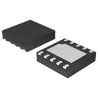
Package: 10 pin TDFN/MLP (suffix EJ)
The A8439 can be used with two Alkaline/NiMH/NiCAD or one
single-cell Li+ battery connected to the transformer primary.
Connect the VIN pin to a 3.0 to 5.5 V supply, which can be
either the system rail or the Li+ battery, if used.
The A8439 is available in a very low profile (0.75 mm)
10-terminal 3×3 mm MLP/TDFN package, making it ideal
for space-constrained applications. It is lead (Pb) free, with
100% matte-tin leadframe plating.
Approximate Scale
Applications include the following:
▪ Digital camera flash
▪ Film camera flash
▪ Cell phone flash
▪ Emergency strobe light
Typical Applications
Two Alkaline/NiMH/NiCAD or one Li+ battery
or 1.5 to 5.5 V
D1
VBATT
T1
+
VBIAS 3.0 to 5.5 V
C1
0.1 μF
R4
100 k7
C2
4.7 μF
R1
VOUT
COUT
One Li+ battery
VBATT or 3.0 to 5.5 V
T1
C1
0.1 μF
R4
C2
4.7 μF
D1
VOUT
R1
COUT
100 k7
R2
VIN
CHARGE
R2
VIN
SW
CHARGE
FB
R5
10 k7
R3
A8439
C3
10 k7
R3
A8439
DONE
TRIGGER
IGBTDRV
GND
TRIGGER
To IGBT Gate
10 k7
Figure 1. Typical circuit with separate power supply to transformer
A8439-DS, Rev. 7
FB
R5
DONE
R6
SW
R6
IGBTDRV
GND
To IGBT Gate
10 k7
Figure 2. Typical circuit with single power supply
C3
�A8439
Photoflash Capacitor Charger with IGBT Driver and Refresh
Selection Guide
Part Number
A8439EEJTR-T
Package
Packing*
10-pin TDFN/MLP
*Contact Allegro for additional packing options
1500 pieces/ 7-in. reel
Absolute Maximum Ratings
Characteristic
Symbol
SW pin
Notes
Rating
Units
V
VSW
–0.3 to 40
VIGBTDRV
–0.3 to VIN + 0.3
V
FB pin
VFB
–0.3 to VIN
V
All other pins
VX
Operating Ambient Temperature
TA
Maximum Junction Temperature
IGBTDRV pin
Storage Temperature
–0.3 to 7
V
–40 to 85
ºC
TJ(max)
150
ºC
Tstg
–55 to 150
ºC
Range E
Package Thermal Characteristics
Characteristic
Package Thermal Resistance
Symbol
RθJA
Test Conditions*
4layer PCB, based on JEDEC standard
Rating Units
45
ºC/W
*Additional information is available on the Allegro website.
Allegro MicroSystems, LLC
115 Northeast Cutoff, Box 15036
Worcester, Massachusetts 01615-0036 (508) 853-5000
www.allegromicro.com
2
�A8439
Photoflash Capacitor Charger with IGBT Driver and Refresh
Functional Block Diagram
SW
DCM
Comparator
VIN
Control Logic
18 µs
CMP3
H→L
Triggered Timer
1.2 V
40 V
DMOS
Q
S SET Q
CMP2
R
CLR Q
ILIM
Comparator
CHARGE
Adjustable
Reference
ILIM Decoder
Enable
FB
CMP1
1.2 V
DONE
VIN
TRIGGER
GND
IGBTDRV
Device Pin-out Diagram
Terminal List Table
Number
1,10
Name
NC
Function
No connection
NC
1
10 NC
IGBTDRV
2
9
FB
VIN
3
8
DONE
3
VIN
Power supply input
GND
4
7
TRIGGER
4
GND
Device ground
CHARGE
5
6
SW
5
CHARGE
6
SW
2
7
8
9
IGBTDRV IGBT driver gate drive output
Charging enable and ISWLIM code input; set to low to power-off
the A8439
Switch, internally connected to the DMOS power FET drain
TRIGGER Strobe signal input
¯D¯¯
O
¯¯
N¯¯
E¯
FB
Open drain, when pulled low by internal MOSFET, indicates that
charging target level has been reached
Output voltage feedback
Allegro MicroSystems, LLC
115 Northeast Cutoff, Box 15036
Worcester, Massachusetts 01615-0036 (508) 853-5000
www.allegromicro.com
3
�A8439
Photoflash Capacitor Charger with IGBT Driver and Refresh
ELECTRICAL CHARACTERISTICS Typical values at TA = 25°C and VIN = 3.3 V (unless otherwise noted)
Characteristics
Symbol
Min.
Typ.
Max. Units
3
–
–
–
1.2
–
–
–
–
–
–
–
–
–
–
–
–
2
–
20
0.2
–
1.5
300
0.01
1.4
1.2
1.0
0.86
0.7
0.55
0.4
0.27
0.27
–
18
18
–
–
–
–
–
5.5
–
600
1
1.6
–
–
–
–
–
–
–
–
1
–
–
1
–
0.8
–
–
V
mA
μA
μA
A
A
A
A
A
A
A
A
Ω
μA
μs
μs
μA
V
V
μs
μs
tILIM(L)
0.2
–
–
μs
tILIM(SU)
–
54
–
μs
¯D¯¯
O
¯¯
N¯¯
E
¯ Output Leakage Current*
IDONELKG
–
–
1
μA
¯D¯¯
O
¯¯
N¯¯
E
¯ Output Low Voltage*
FB Voltage Threshold*
FB Input Current
Auto-Refresh Threshold Level
UVLO Enable Threshold
UVLO Hysteresis
IGBT Driver
IGBTDRV On Resistance to VIN
IGBTDRV On Resistance to GND
TRIGGER Input Current
VDONE(L)
–
–
100
mV
Supply Voltage*
VIN
Supply Current
IIN
Primary Side Current Limit
(ILIM clock input at CHARGE pin)
SW On Resistance
SW Leakage Current*
SW Maximum Off-Time
SW Maximum On-Time
CHARGE Input Current
CHARGE Input Voltage*
ILIM Clock High Time at
CHARGE Pin
ILIM Clock Low Time at
CHARGE Pin
Total ILIM Setup Time
ISWLIM1
ISWLIM2
ISWLIM3
ISWLIM4
ISWLIM5
ISWLIM6
ISWLIM7
ISWLIM8
RDS(On)SW
ISWLKG
tOFF(Max)
tON(Max)
ICHARGE
VCHARGE(H)
VCHARGE(L)
tILIM1(H)
tILIM(H)
VFB
IFB
VFBR
VUVLO
Test Conditions
Charging
Charging done / Refresh monitoring
Shutdown (VCHARGE = 0 V, VTRIGGER = 0 V)
VIN = 3.3 V, ID = 800 mA, TA = 25°C
VSW = 35 V
VCHARGE = VIN
Initial pulse
Subsequent pulses
32 μA into ¯D¯¯
O
¯¯
N¯¯
E¯ pin
1.187
–
–
2.55
–
VFB = 1.205 V
VIN rising
VUVLOHYS
RDS(On)I-V
VIN = 3.3 V, VIGBTDRV = 1.5 V, VTRIGGER = VIN
RDS(On)I-G
VIN = 3.3 V, VIGBTDRV = 1.5 V, VTRIGGER = 0 V
ITRIGGER
VTRIGGER = VIN
VTRIGGER(H)
TRIGGER Input Voltage*
VTRIGGER(L)
Rgate=12 Ω, CLOAD = 6500 pF, VIN = 3.3 V
Propagation Delay, Rising
tDr
Propagation Delay, Falling
tDf
Rgate=12 Ω, CLOAD = 6500 pF, VIN = 3.3 V
Output Rise Time
tr
Rgate=12 Ω, CLOAD = 6500 pF, VIN = 3.3 V
Rgate=12 Ω, CLOAD = 6500 pF, VIN = 3.3 V
Output Fall Time
tf
*Guaranteed by design and characterization over operating temperature range, –40°C to 85°C.
–
–
–
2
–
–
–
–
–
1.205 1.223
–120
–
1.07
–
2.65 2.75
150
–
5
6
–
–
–
30
30
70
70
–
–
1
–
0.8
–
–
–
–
V
nA
V
V
mV
Ω
Ω
μA
V
V
ns
ns
ns
ns
Allegro MicroSystems, LLC
115 Northeast Cutoff, Box 15036
Worcester, Massachusetts 01615-0036 (508) 853-5000
www.allegromicro.com
4
�A8439
Photoflash Capacitor Charger with IGBT Driver and Refresh
Operation Timing Diagram
VIN
CHARGE
SW
VOUT
DONE
TRIGGER
IGBTDRV
A
B
C
D
E
F
Explanation of Events:
A.
Start charging by pulling CHARGE to high, provided that VIN is above the VUVLO level.
B.
¯¯N¯¯E¯ goes low, to signal the
Charging stops when VOUT reaches the target voltage. ¯D¯¯O
completion of the charging process.
C.
When VOUT drops below approximately 90% of target voltage, charging restarts to
replenish the output capacitor (‘auto-refresh’).
D.
When TRIGGER is pulled high, IGBTDRV goes high to fire the IGBT and flash tube.
VOUT drops, and charging restarts to replenish the output capacitor.
E.
If TRIGGER is pulled high during an auto-refresh period, the flash fires normally and the
output capacitor is replenished.
F.
If TRIGGER is pulled high when CHARGE is low, the flash fires normally but the output
capacitor is not replenished.
Allegro MicroSystems, LLC
115 Northeast Cutoff, Box 15036
Worcester, Massachusetts 01615-0036 (508) 853-5000
www.allegromicro.com
5
�A8439
Photoflash Capacitor Charger with IGBT Driver and Refresh
Performance Characteristics
Tests performed using application circuit shown in figure 8
with ISWLIM set to 1.4A (Single rising edge on CHARGE pin), unless otherwise noted
Charging Waveforms
Symbol
C1
C4
t
Conditions
Parameter
VOUT
IBATT(Avg)
time
Parameter
VBATT
VBIAS
COUT
VOUT
Units/Division
50 V
200 mA
1s
Value
2.5 V
3.3 V
100 μF
IBATT
C4
C1
t
VOUT
Symbol
C1
C4
t
Conditions
Parameter
VOUT
IBATT(Avg)
time
Parameter
VBATT
VBIAS
COUT
Units/Division
50 V
200 mA
1s
Value
3.6 V
3.3 V
100 μF
IBATT
C4
C1
t
VOUT
Symbol
C1
C4
t
Conditions
Parameter
VOUT
IBATT(Avg)
time
Parameter
VBATT
VBIAS
COUT
Units/Division
50 V
200 mA
1s
Value
4.2 V
3.3 V
100 μF
IBATT
C4
C1
t
Allegro MicroSystems, LLC
115 Northeast Cutoff, Box 15036
Worcester, Massachusetts 01615-0036 (508) 853-5000
www.allegromicro.com
6
�A8439
Photoflash Capacitor Charger with IGBT Driver and Refresh
Performance Characteristics, continued
Charge Time
Efficiency
VBIAS = 3.3 V, COUT = 100 μF
Connect VBATT to a separate power supply
VBATT = VBIAS , TA = 25°C
90
7 7
80
Efficiency (%)
8 8
Charge Time (s)
Charge Time (s)
Tests performed using application circuit shown in figure 8
with ISWLIM set to 1.4A (Single rising edge on CHARGE pin), unless otherwise noted
6 6
5 5
VVOUT ==320
V
OUT 320 V
4 4
VVOUT ==300
V
OUT 300 V
3 3
2.5
2.5
70
60
50
2 2
2.0
2
VBATT = 5.0 V
VBATT = 4.2 V
VBATT = 3.0 V
33.0 3.53.5 4 4.0 4.5 4.5 5
VVBATT
(V)(V)
BATT
5.0
5.5
5.5
6
40
100
6.0
150
200
VOUT (V)
250
300
350
Typical Switching Waveform
VBATT
C3
VOUT
Symbol
C1
C2
C3
C4
t
Conditions
Parameter
VOUT
VSW
VBATT
IPrimary
time
Parameter
VOUT
VBATT
Units/Division
50 V
10 V
5V
500 mA
2 μs
Value
300 V
VIN
C2
VSW
IPrimary
C4
C1
t
IGBT Drive Timing Definition
TRIGGER
50%
t Dr
IGBTDRV
10%
50%
tr
t Df
90%
90%
tf
10%
Allegro MicroSystems, LLC
115 Northeast Cutoff, Box 15036
Worcester, Massachusetts 01615-0036 (508) 853-5000
www.allegromicro.com
7
�A8439
Photoflash Capacitor Charger with IGBT Driver and Refresh
Performance Characteristics, continued
IGBT Drive waveforms are measured with R-C load (12 Ω, 6800 pF)
IGBT Drive Performance
tr
Rising Signal
VIGBTDRV
Symbol
C2
C3
t
Conditions
Parameter
VIGBTDRV
VTRIGGER
time
Parameter
tDr
tr
CLOAD
Rgate
Units/Division
1V
1V
50 ns
Value
22.881 ns
63.125 ns
6800 pF
12 Ω
C2
VTRIGGER
C3
t
tf
Falling Signal
Symbol
C2
C3
t
Conditions
Parameter
VIGBTDRV
VTRIGGER
time
Parameter
tDf
tf
CLOAD
Rgate
Units/Division
1V
1V
50 ns
Value
27.427 ns
65.529 ns
6800 pF
12 Ω
C2
VIGBTDRV
C3
VTRIGGER
t
Allegro MicroSystems, LLC
115 Northeast Cutoff, Box 15036
Worcester, Massachusetts 01615-0036 (508) 853-5000
www.allegromicro.com
8
�A8439
Photoflash Capacitor Charger with IGBT Driver and Refresh
Functional Description
Overview
Auto-Refresh
The A8439 is a photoflash capacitor charger control IC with
adjustable input current limiting and automatic refresh. It also
integrates an IGBT driver for strobe operation of the flash tube,
dramatically saving board space in comparison to discrete solutions for strobe flash operation. The control logic is shown in the
functional block diagram.
The A8439 features auto-refresh when the feedback resistor
network is connected at the output. Auto-refresh initiates when
the output voltage drops to ≈90 % of the set stop voltage of the
resistor network. The operation is shown in figure 3.
The charging operation of the A8439 is started by a low-to-high
signal on the CHARGE pin, provided that VIN is above VUVLO
level. If CHARGE is already high before VIN reaches VUVLO ,
another low-to-high transition on the CHARGE pin is required
to start the charging. The primary peak current is set by input
clock signals from the CHARGE pin. When a charging cycle is
initiated, the transformer primary side current, IPrimary, ramps up
linearly at a rate determined by the combined effect of the battery
voltage, VBATT , and the primary side inductance, LPrimary. When
IPrimary reaches the current limit, ISWLIM , the internal MOSFET
is turned off immediately, allowing the energy to be pushed into
the photoflash capacitor, COUT, from the secondary winding.
The secondary side current drops linearly as COUT charges. The
recharging cycle starts again, either after the transformer flux
is reset, or after a predetermined time period, tOFF(Max) (18 μs),
whichever occurs first.
The peak current limit can be adjusted to eight different levels,
from 270 mA to 1.4 A, by clocking the CHARGE pin. An internal digital circuit decodes the input clock signals to a counter,
which sets the charging time. This flexible scheme allows the
user to operate the flash circuit according to different battery
input voltages. The battery life can be effectively extended by
setting a lower current limit at low battery voltages.
The output voltage, VOUT, is sensed by a resistor string, R1, R2 ,
and R3 (see application circuit diagrams), connected between
the positive terminal of the output capacitor and ground. This
resistor string forms a voltage divider that feeds back to the FB
pin. The resistors must be sized to achieve a desired output voltage level based on a typical value of 1.205 V at the FB pin. As
soon as VOUT reaches the desired value, the charging process is
terminated. The A8439 automatically starts a new charging cycle
when the internal voltage sensing circuit detects a 10 % drop in
the output voltage. Toggling the CHARGE pin can also start a
refresh operation.
Input Current Limiting
Figure 4 shows the ILIM clock timing scheme protocol. The
total ILIM setup time, tILIM(SU) , denotes the time needed for the
Figure 3. Auto-refresh waveform of A8439.
Allegro MicroSystems, LLC
115 Northeast Cutoff, Box 15036
Worcester, Massachusetts 01615-0036 (508) 853-5000
www.allegromicro.com
9
�A8439
Photoflash Capacitor Charger with IGBT Driver and Refresh
decoder circuit to receive ILIM inputs and set ISWLIM , and has a
minimum duration of 54 μs.
(A) 1.4 A
Figure 5 shows the timing definition of the primary current
limiting circuit. At the end of the setup period, tILIM(SU) , primary
current starts to ramp up to the set ISWIM. The ISWLIM setting
remains in effect as long as the CHARGE pin is high. To reset the
ILIM counter, pull the CHARGE pin low before clocking in the
new setting.
After the first start-up or an ILIM counter reset, each new current
limit can be set by sending a burst of pulses to the CHARGE pin.
The first rising edge starts the ILIM counter, and up to 8 rising
edges will be counted to set the ISWLIM level. The first pulse
width, tILIM1(H), must be at least 20 μs long. Subsequent pulses
(up to 7 more) can be as short as 0.2 μs. The last low-to-high
edge must arrive within 54 μs from the first edge. The CHARGE
pin will stay high afterwards. The four panels of figure 6 show
examples of the pulse streams and the resulting current levels.
(B) 1.2 A
t ILIM(H) ≥ 0.2 μs
t ILIM(L) ≥ 0.2 μs
Clock input at
CHARGE pin
t ILIM1(H) = min.
first pulse width
(C) 1.0 A
t ILIM(SU) = maximum
ILIM setup time
Subsequent rising
edges (0 to 7)
First rising
edge
0 μs
Switching
starts
54 μs
20 μs
Figure 4. ILIM Clock Timing Definition
Start ILIM counter
(D) 0.86 A
Reset ILIM counter
CHARGE
Four rising edges
within t ILIM(SU)
ISWLIM4 = 0.86 A
I SW
Switching
starts
0 μs
20 μs
Switching
stops
54 μs
Figure 5. Current Limit Programming Example (ISWLIM4 selected).
Figure 6. ILIM programming waveforms for ISWLIM = 1.4 A, 1.2 A, 1.0 A,
and 0.86 A.
Allegro MicroSystems, LLC
115 Northeast Cutoff, Box 15036
Worcester, Massachusetts 01615-0036 (508) 853-5000
www.allegromicro.com
10
�A8439
Photoflash Capacitor Charger with IGBT Driver and Refresh
Figure 7 shows the last charging cycle, when the CHARGE pin is
forced low before charging has been completed.
The A8439 implements an adaptive off-time, tOFF , control.
After the switch is turned off, a sensing circuit tracks the flyback
voltage at the SW node. As soon as this voltage swings below
1.2 V, the switch is turned on again for the next charging cycle.
However, when the photoflash capacitor charger circuit starts
up at low output voltage, a timeout may be triggered to limit the
maximum switch off-time to 20 μs.
Figure 7. Last charging cycle, when the CHARGE pin is forced low before
charging is complete.
Allegro MicroSystems, LLC
115 Northeast Cutoff, Box 15036
Worcester, Massachusetts 01615-0036 (508) 853-5000
www.allegromicro.com
11
�A8439
Photoflash Capacitor Charger with IGBT Driver and Refresh
Applications Information
primary inductance, LPrimary (μH), use the following formula:
Transformer Design
Turns Ratio. The minimum transformer turns ratio, N,
(Secondary:Primary) should be chosen based on the following
formula:
VOUT + VD_Drop
N≥
40 − VBATT
(1)
where:
VOUT (V) is the required output voltage level,
VD_Drop (V) is the forward voltage drop of the output diode(s),
VBATT (V) is the transformer battery supply, and
40 (V) is the rated voltage for the internal MOSFET switch,
representing the maximum allowable reflected voltage from the
output to the SW pin.
For example, if VBATT is 3.5 V and VD_Drop is 1.7 V (which could
be the case when two high voltage diodes were in series), and the
desired VOUT is 320 V, then the turns ratio should be at least 8.9.
In a worst case, when VBATT is highest and VD_Drop and VOUT are
at their maximum tolerance limit, N will be higher. Taking VBATT
= 5.5 V, VD_Drop = 2 V, and VOUT = 320 V × 102 % = 326.4 V as
the worst case condition, N can be determined to be 9.5.
In practice, always choose a turns ratio that is higher than the
calculated value to give some safety margin. In the worst case
example, a minimum turns ratio of N = 10 is recommended.
Primary Inductance. As a loose guideline when choosing the
+
C2
4.7 μF
C1
0.1 μF
R4
100 k7
R1
10.0 M7
COUT
100 μF
330 V
R2
FB
10 k7
R3
A8439
78.7 k7
DONE
TRIGGER
IGBTDRV
GND
C3
1 nF
To IGBT Gate
10 k7
(2)
former design should minimize the leakage inductance to ensure
the turn-off voltage spike at the SW node does not exceed the
40 V limit. An achievable minimum leakage inductance for this
application, however, is usually compromised by an increase in
parasitic capacitance. Furthermore, the transformer secondary
capacitance should be minimized. Any secondary capacitance is
multiplied by N 2 when reflected to the primary, leading to high
initial current swings when the switch turns on, and to reduced
efficiency.
Rating
C1
0.1 μF, X5R or X7R, 10 V
C2
4.7 μF, X5R or X7R, 10 V
C3
1 nF, X5R or X7R, 10 V
D1
Fairchild Semiconductor BAV23S
(dual diode connected in series)
T1
Tokyo Coil Engineering T-16-024A,
LPrimary = 12 μH, N = 10.2
SW
R5
.
Leakage Inductance and Secondary Capacitance. The trans-
10.0 M7
VIN
CHARGE
R6
VOUT
1:10.2
300 × 10−9 × VOUT
N × ISWLIM
Ideally, the charging time is not affected by transformer primary inductance. In practice, however, it is recommended that a
primary inductance be chosen between 10 μH and 20 μH. When
LPrimary is lower than 10 μH, the converter operates at higher frequency, which increases switching loss proportionally. This leads
to lower efficiency and longer charging time. When LPrimary is
greater than 20 μH, the rating of the transformer must be dramatically increased to handle the required power density, and the
series resistances are usually higher. A design that is optimized
to achieve a small footprint solution would have an LPrimary of
12 to 14 μH, with minimized leakage inductance and secondary
capacitance, and minimized primary and secondary series resistance. Please refer to the table Recommended Components for
more information.
Symbol
Two Alkaline/NiMH/NiCAD or one Li +
VBATT 1.5 to 5.5 V T1
D1
VBIAS 3.0 to 5.5 V
LPrimary ≥
R1, R2
0805 resistors, 1%
R3
0603 resistor, 1%
R4
Pull-up resistor
R5, R6
Pull-down resistors
Figure 8. Typical circuit for photoflash capacitor charging application.
Allegro MicroSystems, LLC
115 Northeast Cutoff, Box 15036
Worcester, Massachusetts 01615-0036 (508) 853-5000
www.allegromicro.com
12
�A8439
Photoflash Capacitor Charger with IGBT Driver and Refresh
starts to ramp-up. It can be calculated as:
Adjusting Output Voltage
The A8439 senses output voltage continuously in order to provide
auto-refresh function. The output voltage can be adjusted by
selecting proper values of the voltage divider resistors. Use the
following equation to calculate values for Rx (Ω):
R1 + R2 VOUT
=
−1 .
R3
VFB
The peak current of the rectifying diode, ID_Peak, is calculated as:
Output Diode Selection
Choose the rectifying diode(s), D1, to have small parasitic
capacitance (short reverse recovery time) while satisfying the
reverse voltage and forward current requirements.
The peak reverse voltage of the diode, VD_Peak , occurs when the
internal MOSFET switch is closed, and the primary-side current
Recommended Components Table
Component
Rating
0.1 μF, ±10%, 16 V X7R ceramic
C1, Input Capacitor
capacitor (0603)
4.7 μF, ±10%, 10 V, X5R ceramic
C2, Input Capacitor
capacitor (0805)
COUT, Photoflash Capacitor 330 V 100 μF (or 19 to 180 μF)
Input Capacitor Selection
Ceramic capacitors with X5R or X7R dielectrics are recommended for the input capacitor, C2. It should be rated at least
4.7 μF / 6.3 V to decouple the battery input, VBATT , at the primary
of the transformer. When using a separate bias, VBIAS , for the
A8439 VIN supply, connect at least a 0.1 μF / 6.3 V bypass
capacitor to the VIN pin.
Layout Guidelines
Key to a good layout for the photoflash capacitor charger circuit
is to keep the parasitics minimized on the power switch loop
(transformer primary side) and the rectifier loop (secondary side).
Use short, thick traces for connections to the transformer primary
and SW pin.
Output voltage sensing circuit elements must be kept away from
switching nodes such as SW pin. It is important that the ¯D¯¯O¯¯N¯¯E¯
signal trace and other signal traces be routed away from the transformer and other switching traces, in order to minimize noise
pickup. In addition, high voltage isolation rules must be followed
carefully to avoid breakdown failure of the circuit board.
Part Number
Source
GRM188R71C104KA01D
Murata
LMK212BJ475KG
Taiyo Yuden
EPH-331ELL101B131S
Chemi-Con
Philips Semiconductor,
Fairchild Semiconductor
Yageo
Yageo
TDK
Tokyo Coil Engineering
Asatech
D1, Output Diode
2 x 250 V, 225 mA, 5 pF
BAV23S
R1, R2, FB Resistors
R3, FB Resistor
10.0 MΩ, 1/8 W ±1% (0805)
78.7 kΩ 1/10 W ±1% (0603)
1:10.2, LPrimary = 14.5 μH
1:10.2, LPrimary = 12 μH
1:10, LPrimary = 10.8 μH
9C08052A1005FKHFT
9C06031A7872FKHFT
LDT565630T-002
T-16-024A
ST-532517A
T1, Transformer
(5)
ID_ Peak = IPrimary_Peak / N .
(3)
R1 and R2 together need to have a breakdown voltage of at
least 300 V. A typical 0805 surface mount resistor has a 150 V
breakdown voltage rating. It is recommended that R1 and R2
have similar values to ensure an even voltage stress between
them. Recommended values are:
R1 = R2 = 10.0 MΩ (0805 or 1206)
R3 = 78.7 kΩ (0402 or 0603)
which together yield a stop voltage of 305 V.
If desired, larger resistance values may be used to reduce leakage
current from sensing network. (For example: R1=R2=15 MΩ,
and R3 = 118 kΩ.)
(4)
VD_ Peak = VOUT + N × VBATT .
Allegro MicroSystems, LLC
115 Northeast Cutoff, Box 15036
Worcester, Massachusetts 01615-0036 (508) 853-5000
www.allegromicro.com
13
�A8439
Photoflash Capacitor Charger with IGBT Driver and Refresh
Package EJ, 10-Contact TDFN/MLP
0.30
3.00 ±0.15
0.85
0.50
10
10
3.00 ±0.15
1.65
3.10
A
1
2
1
11X
D
SEATING
PLANE
0.08 C
+0.05
0.25 –0.07
C
C
2.38
PCB Layout Reference View
0.75 ±0.05
0.50
1
For Reference Only
(reference JEDEC MO-229WEED)
Dimensions in millimeters
Exact case and lead configuration at supplier discretion within limits shown
2
0.40 ±0.10
1.65
B
10
2.38
A Terminal #1 mark area
B Exposed thermal pad (reference only, terminal #1
identifier appearance at supplier discretion)
C Reference land pattern layout (reference
IPC7351 SON50P300X300X80-11WEED3M);
All pads a minimum of 0.20 mm from all adjacent pads; adjust as
necessary to meet application process requirements and PCB layout
tolerances; when mounting on a multilayer PCB, thermal vias at the
exposed thermal pad land can improve thermal dissipation (reference
EIA/JEDEC Standard JESD51-5)
Copyright ©2005-2013, Allegro MicroSystems, LLC
Allegro MicroSystems, LLC reserves the right to make, from time to time, such departures from the detail specifications as may be required to
permit improvements in the performance, reliability, or manufacturability of its products. Before placing an order, the user is cautioned to verify that
the information being relied upon is current.
Allegro’s products are not to be used in any devices or systems, including but not limited to life support devices or systems, in which a failure of
Allegro’s product can reasonably be expected to cause bodily harm.
The information included herein is believed to be accurate and reliable. However, Allegro MicroSystems, LLC assumes no responsibility for its
use; nor for any infringement of patents or other rights of third parties which may result from its use.
For the latest version of this document, visit our website:
www.allegromicro.com
Allegro MicroSystems, LLC
115 Northeast Cutoff, Box 15036
Worcester, Massachusetts 01615-0036 (508) 853-5000
www.allegromicro.com
14
�