A8480
Boost Regulator for Display Bias or LED Driver
Discontinued Product
These parts are no longer in production The device should not be
purchased for new design applications. Samples are no longer available.
Date of status change: November 2, 2009
NOTE: For detailed information on purchasing options, contact your
local Allegro field applications engineer or sales representative.
Allegro MicroSystems, Inc. reserves the right to make, from time to time, revisions to the anticipated product life cycle plan
for a product to accommodate changes in production capabilities, alternative product availabilities, or market demand. The
information included herein is believed to be accurate and reliable. However, Allegro MicroSystems, Inc. assumes no responsibility for its use; nor for any infringements of patents or other rights of third parties which may result from its use.
�A8480
Boost Regulator for Display Bias or LED Driver
Features and Benefits
Description
▪ Output disconnect during shutdown
▫ 1 μA shutdown current
▪ 2.7 to 9 V input
▫ Operate with 1 or 2 Li+ battery input supply
▪ Output voltage up to 23 V
▪ 1.2 MHz switching frequency
▪ 1.5 A switch current limit
▪ Internal overvoltage and overtemperature protection,
and soft start
The A8480 is a 1.2 MHz optimized boost converter with internal
soft-start and compensation to support WLED, flash/torch,
and display bias applications. The input voltage range of
2.7 to 9 V supports either 1 or 2 Li-ion battery applications.
The high voltage integrated double-diffused MOSFET (DMOS)
allows output voltages as high as 23 V with a switch current
limit of 1.5 A, this increases the maximum quantity of LEDs
that can be used in series.
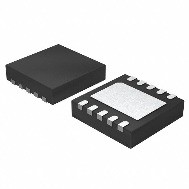
Package:
9-pin CSP (suffix CG)
10-pin MLP/DFN (suffix EJ)
with exposed thermal pad
To maximize battery life in the application, the output can be
completely disconnected from the battery voltage to virtually
eliminate leakage current in the system. The disconnect switch
can pass up to 80 mA current. For system protection, the A8480
has internal overtemperature and overvoltage protection.
The A8480 can be used as a general purpose boost converter
by taking power through the CAP pin. In this configuration, it
can provide up to 520 mA at 12 V with 5.5 V input voltage.
The A8480 is available in both 1.6 mm × 1.6 mm, 0.5 mm
nominal height CSP, and 3 mm × 3 mm, 0.75 mm nominal
height MLP/DFN packages.
Applications include:
▪ WLED flash/torch
▪ WLED backlight
▪ OLED bias supplies
▪ LCD bias supplies
▪ General purpose boost converter
Approximate Scale 1:1
Typical Applications
L1
22 μH
MBRA130LT3
VOUT
L1
VOUT
D1
B1[3]
EJ only
A8480
[1] [PGND]
B2[2]
VSUPPLY
2.8 to 5 V
VIN
C1[4]
C2[5]
CAP
FB[FB1]
OUT1
RADJ
12.1 kΩ
CIN
1 μF
6.3 V
SW
FBADJ
DIM
GND
ON1
D1
B1[3]
A3[10]
EJ only
VIN
A8480
[1] [PGND]
A2[9]
COUT
2.2 μF
16 V
B3[8]
A1[7]
B2[2]
VSUPPLY
C1[4]
CIN
C3[6]
C2[5]
48 kΩ
SW
CAP
FB[FB1]
OUT1
FBADJ
GND
DIM
ON1
A3[10]
A2[9]
COUT
B3[8]
A1[7]
30 Ω
Square brackets indicate pin names or numbers used only with the EJ package;
where no brackets are shown with a pin name, name applies to both CG and EJ packages
Figure 1. Using the A8480 to drive a flash (100 mA) or
torch (20 mA)
8480-DS, Rev. 4
R1
C3[6]
R2
Square brackets indicate pin names or numbers used only with the EJ package;
where no brackets are shown with a pin name, name applies to both CG and EJ packages
Figure 2. The A8480 used as a general boost
�A8480
Boost Regulator for Display Bias or LED Driver
Functional Block Diagram
VIN
VREF1
SW
Error Amplifier
0.6 V
C2
S1
FB
[EJ only: FB1]
C4
R
Q
Driver
S
Soft
Start
∑
C1
PGND
Ramp
Clock
Oscillator
CG only
VCAP
UVLO
Temp
EJ only
CAP
Fault
Protection
S2
OUT1
ON1
On/Off
Logic
DIM
FBADJ
S3
PAD
GND
EJ only
Absolute Maximum Ratings
Package Thermal Characteristics
Input or Output Voltage
SW, CAP, OUT1, FBADJ pins .................................–0.3 to 26 V
VIN pin, VIN .............................................................–0.3 to 9.5 V
All other pins, Vx ....................... –0.3 to VIN + 0.3 V (7 V max.)
Operating Ambient Temperature, TA ................................ –40°C to 85°C
Maximum Junction Temperature, TJ(max) ...................................... 150°C
Storage Temperature, Tstg ............................................. –55°C to 150°C
CG package: 109 °C/W, on a 2-sided board. Please refer to
page 14 for test board layout.
EJ package: RθJA = 45 °C/W, on a 4-layer board.
Additional information is available on the Allegro Web site.
Packages are lead (Pb) free.
EJ package has 100% matte tin leadframe plating.
Selection Guide
Part Number
Package
Packinga
A8480ECGLT-Tb
9-bump chip scale package
Tape and Reel
A8480EEJTR-T
10-pin MLP/DFN package
aContact Allegro
1500 pieces per reel
for additional packing options.
bContact Allegro factory for availability.
Allegro MicroSystems, Inc.
115 Northeast Cutoff
Worcester, Massachusetts 01615-0036 U.S.A.
1.508.853.5000; www.allegromicro.com
2
�A8480
Boost Regulator for Display Bias or LED Driver
Pin-out Diagrams
1
10
A3
A2
A1
2
B3
B2
B1
3
C3
C2
C1
4
7
5
6
CG Package
(Top View)
9
PAD
8
EJ Package
(Top View)
Terminal List Table
Number
CG
EJ
Name
Description
–
1
PGND
A1
–
GND
Power and signal ground connection; connect directly to the ground plane.
Power ground connection; use to avoid interference with signal ground.
–
7
GND
Signal ground reference; connect directly to the ground plane.
A2
9
CAP
This is the connection to the output capacitor for the boost regulator output.
A3
10
SW
This is the connection between the internal boost switch and the external inductor.
Because rapid changes of current occur at this pin, the board traces connected to this pin
should be minimized and the inductor and diode should be connected as close to this pin
as possible.
B1
3
VIN
This is the power input supply connection to the circuit. A bypass capacitor tying this pin
to GND must be connected close to this pin.
B2
–
FB
–
2
FB1
B3
8
OUT1
This is the voltage-controlled output pin for the OLED drive. An internal switch
disconnects the OLED during shutdown.
C1
4
FBADJ
Open collector output driven by DIM. This can be used to provide dimming by connecting
an additional feedback circuit or it can be used to drive external output.
C2
5
DIM
Logic input. Driving DIM puts the FBADJ open collector output low.
C3
6
ON1
This is the enable pin for OUT1.
–
PAD
–
This is the feedback pin for controlling voltage on the OUT1 pin. The nominal reference
voltage on this pin is 600 mV. In order to minimize noise, connect the feedback resistor
network close to this pin.
Exposed thermal pad. Connect to GND plane for enhanced thermal performance.
Allegro MicroSystems, Inc.
115 Northeast Cutoff
Worcester, Massachusetts 01615-0036 U.S.A.
1.508.853.5000; www.allegromicro.com
3
�A8480
Boost Regulator for Display Bias or LED Driver
ELECTRICAL CHARACTERISTICS at TA = 25°C, VIN = ON1 = DIM = 3.0 V (unless noted otherwise)
Characteristics
Input Voltage Range
Quiescent Input Current
Undervoltage Lockout Threshold
Feedback Reference Voltage
Symbol
IIN(Q)
VUVLO
Switch Current Limit
DIM=ON1=0
VIN rising
VFB
2.7 V ≤ VIN ≤ 9 V
Min.
Typ.
Max.
Units
2.7
–
9
V
–
–
1
μA
2.25
2.45
2.60
V
584
610
636
mV
–
0.1
–
%/V
IFB
–
45
100
nA
ISWLim
–
1.5
–
A
Feedback Voltage Line Regulation
Feedback Input Current
Test Conditions
VIN
Switch Frequency
fSW
1
1.2
1.4
MHz
Switch Maximum Duty Cycle*
DC
85
90
–
%
ISW = 0.5 A
–
225
–
mΩ
Switch S1 On Resistance
RDS(on)1
Switch S2 On Resistance
RDS(on)2
ISW = 80 mA
–
3.5
–
Ω
Switch S1 Leakage Current
ISW(lkg)1
VSW = 5 V
–
–
1
μA
Switch S2 Leakage Current
ISW(lkg)2
–
–
1
μA
FBADJ MOSFET On Resistance
RDSF(on)
VDIM > VIH
–
10
–
Ω
FBADJ MOSFET Leakage Current
IFBADJ(lkg)
VDIM < VIL , VFBADJ = 0.6 V
–
1
–
μA
ON1, DIM Input Threshold Low
VIL
–
–
0.4
V
ON1, DIM Input Threshold High
VIH
1.5
–
–
V
ON1, DIM Input Bias Current
IIB
–
65
–
μA
Output Overvoltage Rising Limit
VOVPR
–
24.5
25.5
V
Thermal Shutdown Threshold
TSHDN
–
160
–
°C
Thermal Shutdown Hysteresis
TSHDNhys
–
10
–
°C
–
2
–
ms
Soft-Start Period
tSS
VOUT = 10 V
*Guaranteed by design.
Allegro MicroSystems, Inc.
115 Northeast Cutoff
Worcester, Massachusetts 01615-0036 U.S.A.
1.508.853.5000; www.allegromicro.com
4
�A8480
Boost Regulator for Display Bias or LED Driver
Performance Characteristics
Tests performed using application circuit shown in figure 5
L1 = 4.7 μH, CIN = COUT = 1 μF, TA = 25°C (unless otherwise noted)
Efficiency versus Load Current
VOUT = 12 V
90.00
1.00
0.50
80.00
VIN
(V)
75.00
5.0
4.2
70.00
3.3
2.5
65.00
Load Regulation (%)
85.00
Efficiency (%)
Load Regulation
VOUT = 12 V
0
-0.50
55.00
-2.50
20
40
60
4.2
3.3
3.6
2.5
3.0
-1.50
-2.00
0
5.0
4.2
-1.00
60.00
50.00
VIN
(V)
-3.00
80
0
20
Efficiency versus Load Current
VOUT = 15 V
90.00
80
0.50
VIN
(V)
75.00
5.0
4.2
70.00
3.3
2.5
65.00
Load Regulation (%)
80.00
Efficiency (%)
60
Load Regulation
VOUT = 15 V
1.00
85.00
0
VIN
(V)
-0.50
5.0
4.2
-1.00
3.6
3.0
-1.50
60.00
-2.00
55.00
-2.50
50.00
-3.00
0
20
40
60
0
80
20
Efficiency versus Load Current
VOUT = 18 V
90.00
40
60
80
IOUT (mA)
Load Current (mA)
Load Regulation
VOUT = 18 V
1.00
85.00
VIN
(V)
75.00
5.0
4.2
70.00
3.3
2.5
65.00
60.00
Load Regulation (%)
0.50
80.00
Efficiency (%)
40
IOUT (mA)
Load Current (mA)
0
VIN
(V)
-0.50
5.0
4.2
-1.00
3.6
3.0
-1.50
-2.00
55.00
-2.50
50.00
0
20
40
60
Load Current (mA)
80
-3.00
0
20
40
60
80
IOUT (mA)
Allegro MicroSystems, Inc.
115 Northeast Cutoff
Worcester, Massachusetts 01615-0036 U.S.A.
1.508.853.5000; www.allegromicro.com
5
�A8480
Boost Regulator for Display Bias or LED Driver
Performance Characteristics
Tests performed using application circuit shown in figure 5
L1 = 4.7 μH, CIN = COUT = 1 μF, TA = 25°C (unless otherwise noted)
Line Regulation
VOUT = 12 V
1.00
Startup
IL
Line Regulation (%)
0.50
Dimming
Level
(mA)
0
VOUT1
C1
0
-0.50
20
40
-1.00
60
VSW
C2
80
-1.50
-2.00
C3
-2.50
VON1
-3.00
2.5
3.3
4.2
5
7
9
C4
VIN (V)
t
Symbol
C1
C2
C3
C4
t
Conditions
Line Regulation
VOUT = 15 V
1.00
Line Regulation (%)
0.50
Dimming
Level
(mA)
0
0
-0.50
20
-1.00
Parameter
IL
VOUT1
VSW
VON1
time
Parameter
VIN
VOUT
IOUT
Units/Division
500 mA
10.0 V
10.0 V
2.00 V
1 ms
Value
3.3 V
18 V
80 mA
40
60
-1.50
80
Shutdown
-2.00
-2.50
IL
-3.00
2.5
3.3
4.2
5
7
9
C1
VIN (V)
Line Regulation
VOUT = 18 V
0.50
VSW
C3
0
Line Regulation (%)
VOUT1
C2
Dimming
Level
(mA)
-0.50
0
-1.00
VON1
C4
t
20
-1.50
40
60
-2.00
80
-2.50
-3.00
-3.50
2.5
3.3
4.2
5
VIN (V)
7
9
Symbol
C1
C2
C3
C4
t
Conditions
Parameter
IL
VOUT1
VSW
VON1
time
Parameter
VIN
VOUT
IOUT
Units/Division
500 mA
10.0 V
10.0 V
2.00 V
5 ms
Value
3.3 V
18 V
80 mA
Allegro MicroSystems, Inc.
115 Northeast Cutoff
Worcester, Massachusetts 01615-0036 U.S.A.
1.508.853.5000; www.allegromicro.com
6
�A8480
Boost Regulator for Display Bias or LED Driver
Performance Characteristics
Efficiency and load regulation for general boost without disconnect FET
Tests performed using application circuit shown in figure 2
Efficiency versus Load Current
VIN = 3.3 V
90
0
–0.2
88
86
VOUT
(V)
84
Load Regulation (%)
Efficiency (%)
Load Regulation
VIN = 3.3 V
12
82
15
80
18
78
–0.4
12
–0.8
18
–1.2
74
–1.4
0
50
100
–1.6
150
15
–1.0
76
72
VOUT
(V)
–0.6
0
50
Efficiency versus Load Current
VIN = 5 V
94
150
Load Regulation
VIN = 5 V
0.8
0.6
92
0.4
90
88
86
Load Regulation (%)
VOUT
(V)
12
84
15
82
18
80
78
76
0.2
VOUT
(V)
0
–0.2
12
–0.4
15
–0.6
18
–0.8
–1.0
74
–1.2
72
–1.4
70
–1.6
0
20 40 60 80 100 120 140 160 180 200 220 240 260
0
20
40
60
80 100 120 140 160 180 200 220 240 260
IOUT (mA)
Load Current (mA)
Maximum Output Current versus Input Voltage
Without Disconnect Switch
600
Output Current (mA)
Efficiency (%)
100
IOUT (mA)
Load Current (mA)
500
VOUT
(V)
400
12
15
300
18
200
100
0
2.5
3.0
3.5
4.0
4.5
5.0
5.5
Input Voltage (V)
Allegro MicroSystems, Inc.
115 Northeast Cutoff
Worcester, Massachusetts 01615-0036 U.S.A.
1.508.853.5000; www.allegromicro.com
7
�A8480
Boost Regulator for Display Bias or LED Driver
Functional Description
The A8480 is a boost converter with output disconnect. The boost
stage boosts input battery voltage to a sufficient level to drive
an OLED or a set of series-connected WLEDs. This stage uses
1.2 MHz constant frequency, current mode control. Typical application circuits are shown in figure 1, and the Typical Applications
section.
When OUT1 is enabled and VIN is greater than VIN (min), the
boost stage is ramped-up with soft start, with switch, S2, completely turned on.
The A8480 provides protection against output overvoltage on the
CAP pin, overload, and overtemperature. Also, it has an input
undervoltage lockout to avoid malfunction and battery drain.
At light loads, instantaneous inductor current drops to zero. This
is known as discontinuous mode operation and will result in some
low frequency ripple. In discontinuous mode, the voltage at the
SW pin will ring, due to the resonant LC circuit formed by the
The constant voltage drive for OLED is provided through the
OUT1 pin. The internal switch between the CAP and OUT1 pins
disconnects the OLED when OUT1 is disabled.
inductor and the switch and diode capacitance. This ringing is
For driving OLEDs, output voltage is sensed by the FB1 pin
through a voltage divider network. Output voltage (V) is set as:
R1 + R2
VOUT1 = 0.61 ×
R2
(1)
recommended.
When DIM is high and RFBADJ is used (R2 is configured in
parallel with RFBADJ in the circuit; see figure 5a), the output
voltage is set as follows:
R1 +
VOUT1 = 0.61 ×
R2 + RFBADJ
R2 × RFBADJ
R2 + RFBADJ
tor across the inductor, but this will reduce efficiency and is not
Dual OLED Application
The A8480 can be easily used as a dual OLED driver. In this
application, the main OLED can be connected to OUT1 and the
sub OLED can be connected between the output of the boost
stage, at VOUT , and the FBADJ pin, as in the application shown
R2 × RFBADJ
low frequency and is not harmful. It can be damped with a resis-
in figure 6. The sub OLED is controlled by the DIM pin. Pulling
(2)
the DIM pin high turns on the internal switch S3, which pulls
the FBADJ pin low, allowing the sub OLED to turn on. Figure 6
shows that the sub OLED is grounded as well.
Allegro MicroSystems, Inc.
115 Northeast Cutoff
Worcester, Massachusetts 01615-0036 U.S.A.
1.508.853.5000; www.allegromicro.com
8
�A8480
Boost Regulator for Display Bias or LED Driver
Applications Information
Component Selection
The component values shown in the application circuits will
be sufficient for most applications (typical application circuits
are shown in figure 1, and the Typical Applications section). To
reduce the output ripple, the output inductor may be increased in
value, but in most cases this will result in excessive board area
and cost.
Inductor Selection
The inductor is the most important component in the power
supply design because it affects the steady-state performance,
transient response, and loop stability. The inductance value, DC
resistance, and the saturation current should be considered when
choosing the inductor. The DC current of the inductor can be
calculated by:
IL_DC =
VOUT IOUT
VIN η
(3)
and the inductance value can be calculated by:
⎛
⎞
V
1
⎜⎜1 – imin ⎟⎟
(4)
V
f
OUT
⎝
⎠
where ∆i = (20% to 40%) × IL_DC is the peak-to-peak ripple current.
Lmin =
Vimin
∆i η
Smaller inductance values force the converter into discontinuous
mode, which will reduce the maximum output current. Larger
inductance values reduce the gain and phase margin, which will
result in instability of the loop.
The inductor should have low winding resistance, typically
< 0.2 Ω and low 1.2 MHz core loss for better efficiency.
The inductor should have a saturation current higher than 1.5 A,
in order to provide 20 V at the OUT1 pin, and 100 mA at 2.7 VIN.
For high temperature operation, a suitable derating factor should
be considered. Several inductor manufacturers, including:
Coilcraft, Murata, Panasonic, Sumida, Taiyo Yuden, and TDK,
have and are developing suitable small-size inductors.
Diode Selection
The diode should have a low forward voltage to reduce conduction losses and a low capacitance to reduce switching losses.
Schottky diodes can provide both of these features, if carefully
selected. The forward voltage drop is a natural advantage for
Schottky diodes and decreases as the current rating increases.
However, as the current rating increases, the diode capacitance
also increases, so the optimum selection is usually the lowest current rating above the circuit maximum.
The diode RMS current rating should be:
⎯⎯
IDIODE(RMS) = IOUT = IIN √ 1–D
.
(5)
Diode PIV should be higher than the output voltage on the CAP
pin.
Capacitor Selection
The input capacitor selection is based on the input voltage ripple.
It can be calculated as:
CIN(min) =
8
fSW
∆i
VIN(ripple)
(6)
where VIN(ripple) is the input ripple.
The output capacitor selection is based on the output ripple
requirement. It can be calculated by:
COUT =
VOUT –VIN
VOUT
1
f
IOUT
Vripple(pp)
(7)
where Vripple is the peak-to-peak output ripple.
In addition, the ESR-related output ripple can be calculated by:
Vripple(ESR) = IOUT
ESR
.
(8)
If a ceramic capacitor is selected, the ESR-related ripple can be
neglected, due to the low ESR. If a tantalum electrolytic capacitor
is selected, this portion of ripple voltage has to be considered.
During load transient response, a larger output capacitance
always helps to supply or absorb additional current, which results
in lower overshoot and undershoot voltage.
Because the capacitor values are low, ceramic capacitors are the
best choice for this application. To reduce performance variation
over temperature, low drift types such as X7R and X5R should
be used. Recommended specifications are shown in the table
below. Suitable capacitors are available from TDK, Taiyo Yuden,
Murata, Kemet, and AVX.
The output capacitor is placed on the CAP pin only. An additional
capacitor can be added on the OUT1 pin, but it is not needed for
proper operation and it cannot replace the capacitor on the CAP pin.
Allegro MicroSystems, Inc.
115 Northeast Cutoff
Worcester, Massachusetts 01615-0036 U.S.A.
1.508.853.5000; www.allegromicro.com
9
�A8480
Boost Regulator for Display Bias or LED Driver
Typical Application Circuits
L1
10 μH
+5 V
BAT54S
CS1
1 μF
25 V
BAT54S
VOUT2
–7.5 V
R3
3.3 kΩ
D3
CS4
2.2 μF
16 V
D4
7.5 V
CS5
2.2 μF
16 V
CS3
1 μF
25 V
D2
VOUT1
8.75 V
50 mA
D1
A1[1]
B1[3]
A8480
GND[PGND]
C2[5]
B2[2]
SW
CAP
VIN
[7] [GND]
COUT
A3[10]
A2[9]
Square brackets indicate pin names or numbers
used only with the EJ package; where no brackets
are shown with a pin name, name applies to
both CG and EJ packages
FBADJ C1[4]
DIM
OUT1
ON1
FB[FB1]
R4
512 kΩ
VSW
CIN
EJ only
CS2
1 μF
25 V
B3[8]
R1
820 kΩ
C3[6]
R2
61.9 kΩ
Figure 3a. Dual outputs (VOUT and –VOUT)
CS2
1 μF
25 V
BAT54S
CS1
1 μF
25 V
BAT54S
CS6
1 μF
25 V
R3
3.3 kΩ
CS4
2.2 μF
16 V
D2
D5
BAT54S
D4
7.5 V
CS5
2.2 μF
16 V
VOUT3
R4
512 kΩ –7.5 V
D6
16 V
CS8
2.2 μF
16 V
R6
15 kΩ
CS3
1 μF
25 V
R5
1 kΩ
CS7
2.2 μF
16 V
VOUT2
+15 V
VSW
+5 V
L1
10 μH
CIN
A8480
A1[1]
GND[PGND]
B1[3]
EJ only
D3
VIN
[7] [GND]
C2[5]
B2[2]
DIM
FB[FB1]
D1
SW
CAP
COUT
A3[10]
A2[9]
OUT1
FBADJ C1[4]
ON1
R1
820 kΩ
VOUT1
8.75 V
50 mA
Square brackets indicate pin names or numbers
used only with the EJ package; where no brackets
are shown with a pin name, name applies to
both CG and EJ packages
C3[6]
R2
61.9 kΩ
Figure 3b. Triple outputs (VOUT , –VOUT , and 2VOUT)
Allegro MicroSystems, Inc.
115 Northeast Cutoff
Worcester, Massachusetts 01615-0036 U.S.A.
1.508.853.5000; www.allegromicro.com
10
�A8480
Boost Regulator for Display Bias or LED Driver
D0
VIN
[1]
CIN
[PGND]
B2[2]
FB[FB1]
C1[4]
EJ only
Li+
Battery
2.7 to 5.5 V
A8480
FBADJ
C2[5]
D1
SW
CAP
OUT1
GND
DIM
ON1
DZ
A3[10]
Efficiency versus Input Voltage
D2
74
73
A2[9]
72
B3[8]
COUT
A1[7]
D9
η (%)
B1[3]
VOUT
L1B 10 μH
L1A 10 μH
71
70
69
D10
C3[6]
68
67
2.5
3.0
3.5
R2
30Ω
4.0
4.5
5.0
5.5
VIN (V)
L1A, L1B 744878100; Wurth Electronics
D0
BAT400D-7
DZ
IN4747ADICT
Square brackets indicate pin names or numbers used only with the EJ package;
where no brackets are shown with a pin name, name applies to both CG and EJ packages
Figure 4. Using the A8480 to drive 10 white LEDs (WLED)
VOUT
L1
CIN
B2[2]
VIN
D1
A8480
FB[FB1]
SW
CAP
RADJ
C1[4] FBADJ
[1] [PGND]
Li+
Battery
GND
ON1
COUT
A2[9]
ON1
B3[8]
A1[7]
C3[6]
DIM
R1
EJ only
C2[5] DIM
OUT1
A3[10]
OLED
B1[3]
R2
VOUT
Square brackets indicate pin names or numbers used only with the EJ package;
where no brackets are shown with a pin name, name applies to both CG and EJ packages
Figure 5a. Typical application circuit for A8480
driving an OLED with dimming.
Figure 5b. Timing diagram for circuit shown in
figure 5a.
Allegro MicroSystems, Inc.
115 Northeast Cutoff
Worcester, Massachusetts 01615-0036 U.S.A.
1.508.853.5000; www.allegromicro.com
11
�A8480
Boost Regulator for Display Bias or LED Driver
VOUT
L1
B1[3]
FB[FB1]
C1[4]
FBADJ
SW
CAP
OUT1
GND
COUT
A3[10]
A2[9]
B3[8]
R3
A1[7]
R1
DIM
ON1
C3[6]
R2
OLED
Sub
C2[5]
OLED
Main
EJ only
B2[2]
D1
A8480
[1] [PGND]
CIN
Li+
Battery
VIN
R4
Square brackets indicate pin names or numbers used only with the EJ package;
where no brackets are shown with a pin name, name applies to both CG and EJ packages
Figure 6. Main and sub OLED bias with both grounded
VBATT
+8 to 16 V
VOUT
A1[1]
VIN
+5 V
B2[2]
B1[3]
C1[4]
C2[5]
D1
A8480
GND[PGND]
FB[FB1]
VIN
FBADJ
DIM
SW
COUT
R1
Efficiency versus Input Voltage
R3
A3[10]
95
CAP
A2[9]
OUT1 B3[8]
[GND]
ON1
[7]
96
R2
EJ only
94
18 V
R4
C3[6]
300
00 mA
93
η (%)
CIN
OLED
L1
92
91
250 mA
90
89
200 mA
88
87
8
Square brackets indicate pin names or numbers used only with the EJ package;
where no brackets are shown with a pin name, name applies to both CG and EJ packages
10
12
14
16
VBATT (V)
Figure 7. OLED supply for GPS/Auto Infotainment,
with external output disconnect FET
Allegro MicroSystems, Inc.
115 Northeast Cutoff
Worcester, Massachusetts 01615-0036 U.S.A.
1.508.853.5000; www.allegromicro.com
12
�A8480
Boost Regulator for Display Bias or LED Driver
VOUT
L1
B1[3]
CIN
[1] [PGND]
EJ only
B2[2]
3V
VIN
D1
A8480
CAP
FB[FB1]
A3[10]
A2[9]
COUT
OUT1 B3[8]
C1[4] FBADJ
C2[5]
SW
GND
DIM
ON1
A1[7]
3.4 V
250 mA
C3[6]
R2
2.5Ω
Square brackets indicate pin names or numbers used only with the EJ package;
where no brackets are shown with a pin name, name applies to both CG and EJ packages
Figure 8. A8480 driving high current flash/torch LEDs
D1
MBR0530T1
L1
22 μH
12 V
C1
1 μF
VOUT
D1
B1[3]
EJ only
VIN
A8480
[1] [PGND]
C2[5]
DIM
C1[4] FBADJ
5V
B2[2]
CIN
1 μF
FB[FB1]
SW
CAP
OUT1
GND
ON1
A3[10]
A2[9]
C2
1 μF
B3[8]
A1[7]
C3[6]
30 Ω
30 Ω
30 Ω
Square brackets indicate pin names or numbers used only with the EJ package;
where no brackets are shown with a pin name, name applies to both CG and EJ packages
Figure 9. A8480 driving 21-LED frame for digital photograph display
Allegro MicroSystems, Inc.
115 Northeast Cutoff
Worcester, Massachusetts 01615-0036 U.S.A.
1.508.853.5000; www.allegromicro.com
13
�A8480
Boost Regulator for Display Bias or LED Driver
Thermal Performance
The A8480 CSP package has low thermal impedance, RθJA = 109 °C/W.
This data was taken from tests performed on the CSP demonstration board.
The board layout is presented here for reference (enlarged for clarity).
Top layer
Bottom layer
Allegro MicroSystems, Inc.
115 Northeast Cutoff
Worcester, Massachusetts 01615-0036 U.S.A.
1.508.853.5000; www.allegromicro.com
14
�A8480
Boost Regulator for Display Bias or LED Driver
Package CG, 9-Pin CSP
1.605
3
2
1
3
A
2
1
A
A
B
B
1.625
1.00
0.50
C
C
�X
�.25
0.50
1.00
SEATING
PLANE
C
C
9X
PCB Layout Reference View
0.05 C
0.50
0.255
All dimensions nominal, not for tooling use
Dimensions in millimeters
Dimensions exclusive of burrs
Exact configuration at supplier discretion within limits shown
C
B
A
1.00
0.50
0.312
B
3
2
1
0.50
A Terminal #1 mark area
B Die orientation mark
C
Reference pad layout; all pads a minimum of 0.20 mm from
all adjacent pads; adjust as necessary to meet application
process requirements and PCB layout tolerances
0.302
1.00
Allegro MicroSystems, Inc.
115 Northeast Cutoff
Worcester, Massachusetts 01615-0036 U.S.A.
1.508.853.5000; www.allegromicro.com
15
�A8480
Boost Regulator for Display Bias or LED Driver
Package EJ, 10-Pin MLP/DFN
0.30
3.00
0.85
0.50
10
10
3.00
1.65
3.10
A
1
2
1
11X
D
2.38
0.75
0.08 C
C
0.25
PCB Layout Reference View
0.50
1
All dimensions nominal, not for tooling use
(reference JEDEC MO-229WEED)
Dimensions in millimeters
Exact case and lead configuration at supplier discretion within limits shown
2
0.40
1.65
B
10
2.38
A Terminal #1 mark area
B Exposed thermal pad (reference only, terminal #1
identifier appearance at supplier discretion)
C Reference land pattern layout (reference IPC7351
SON50P300X300X80-11WEED3M);
All pads a minimum of 0.20 mm from all adjacent pads; adjust as
necessary to meet application process requirements and PCB layout
tolerances; when mounting on a multilayer PCB, thermal vias at the
exposed thermal pad land can improve thermal dissipation (reference
EIA/JEDEC Standard JESD51-5)
D Coplanarity includes exposed thermal pad and terminals
Copyright ©2007, Allegro MicroSystems, Inc.
The products described here are manufactured under one or more U.S. patents or U.S. patents pending.
Allegro MicroSystems, Inc. reserves the right to make, from time to time, such departures from the detail specifications as may be required to permit improvements in the performance, reliability, or manufacturability of its products. Before placing an order, the user is cautioned to verify that the
information being relied upon is current.
Allegro’s products are not to be used in life support devices or systems, if a failure of an Allegro product can reasonably be expected to cause the
failure of that life support device or system, or to affect the safety or effectiveness of that device or system.
The information included herein is believed to be accurate and reliable. However, Allegro MicroSystems, Inc. assumes no responsibility for its use;
nor for any infringement of patents or other rights of third parties which may result from its use.
For the latest version of this document, visit our website:
www.allegromicro.com
Allegro MicroSystems, Inc.
115 Northeast Cutoff
Worcester, Massachusetts 01615-0036 U.S.A.
1.508.853.5000; www.allegromicro.com
16
�