A8498
Wide Input Voltage 3.0 A Step Down Regulator
FEATURES AND BENEFITS
•
•
•
•
•
DESCRIPTION
8 to 50 V input range
Integrated DMOS switch
Adjustable fixed off-time
Highly efficient
Adjustable 0.8 to 24 V output
The A8498 is a step down regulator that will handle a wide
input operating voltage range.
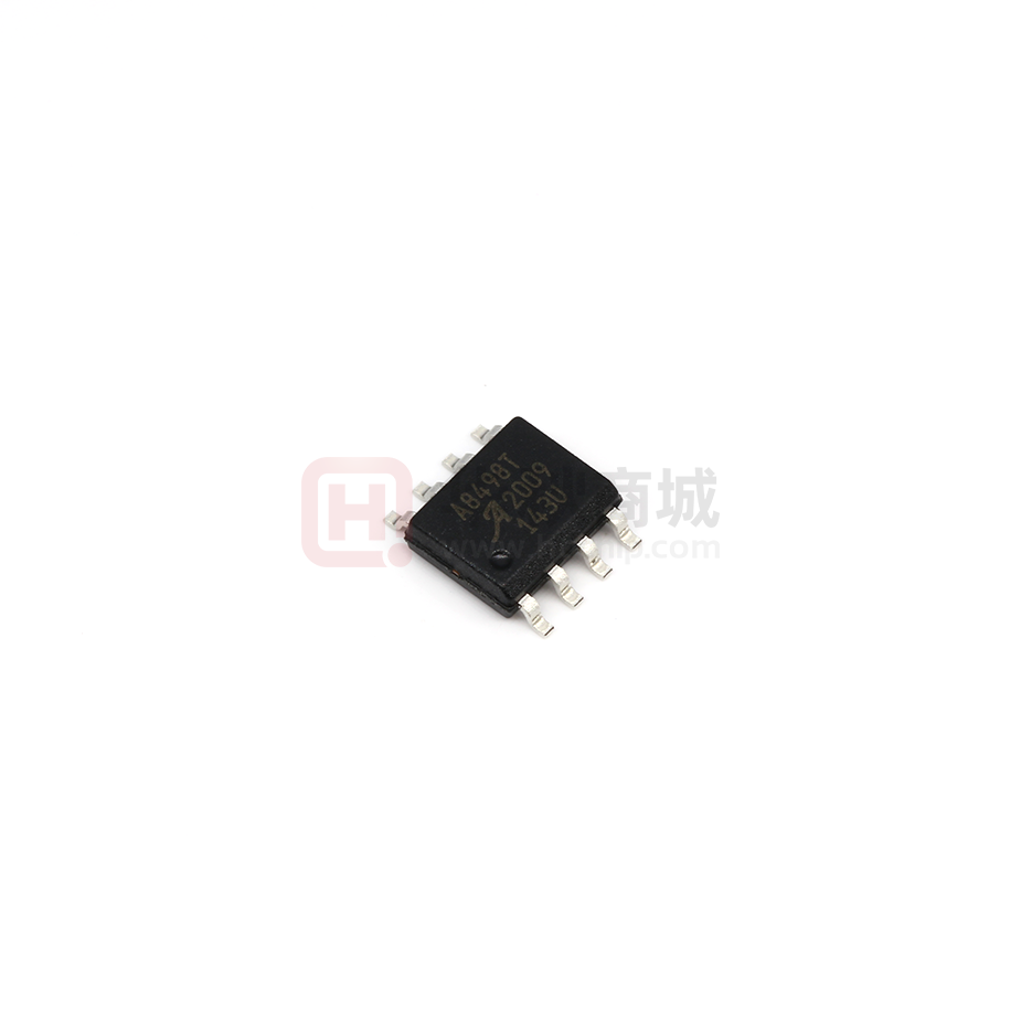
The A8498 is supplied in a low-profile 8-lead SOIC with
exposed pad (package LJ). Applications include:
• Applications with 8 to 50 V input voltage range needing
buck regulator for 3.0 A output current
• Consumer equipment power
• Uninterruptible power supplies (lead acid battery
charger)
• Automotive telematics: 9 to 16 V input, with higher
voltage protection
• 12 V lighter-powered applications (portable DVD, etc.)
• Point of Sale (POS) applications
• Industrial applications with 24 or 36 V bus
Package: 8-Lead SOIC with Exposed Thermal Pad (suffix LJ)
Approximate Scale 1:1
+42 V
CBOOT
0.01 µF
ENB
TSET
CIN2
220 µF
50 V
VIN
A8498
LX
L1
68 µH
VOUT
3.3 V / 3 A
VBIAS
RTSET
63.4 kΩ
R1
6.34 kΩ
GND
CIN1
0.22 µF
FB
D1
R2
2 kΩ
ESR
COUT
220 µF
25 V
Efficiency %
BOOT
Efficiency vs. Output Current
90.0
88.0
86.0
84.0
82.0
80.0
78.0
76.0
74.0
72.0
70.0
VOUT (V)
5
3.3
0
Typical Application
500
1000
1500
2000
2500
IOUT (mA)
Circuit for 42 V step down to 3.3 V at 3 A. Efficiency data from circuit shown in left panel. Data is for reference only.
A8498-DS, Rev. 7
3000
�A8498
Wide Input Voltage 3.0 A Step Down Regulator
SPECIFICATIONS
Ordering Information
Use the following complete part numbers when ordering:
Part Numbera
A8498SLJTR-T
aLeadframe
Packingb
Description
13 in. reel, 3000 pieces/reel
LJ package, SOIC surface mount with
exposed thermal pad
plating 100% matte tin.
for additional packing options.
bContact Allegro
Absolute Maximum Ratings
Characteristic
Load Supply Voltage, VIN pin
Input Voltage, VBIAS pin
Switching Voltage
Input Voltage Range, ENB pin
Operating Ambient Temperature Range
Symbol
Conditions
Min.
Typ.
Max.
Units
VIN
–
–
50
V
VBIAS
–0.3
–
7
V
VS
–1
–
–
V
VENB
–0.3
–
7
V
TA
–20
–
85
°C
Junction Temperature
TJ(max)
–
–
150
°C
Storage Temperature
TS
–55
–
150
°C
*Output current rating may be limited by duty cycle, ambient temperature, and heat sinking. Under any set of conditions, do not exceed the specified current ratings, or a
junction temperature, TJ, of 150°C.
Package Thermal Characteristics*
Package
RθJA
(°C/W)
PCB
LJ
35
4-layer
* Additional information is available on the Allegro website.
Allegro MicroSystems, LLC
115 Northeast Cutoff
Worcester, Massachusetts 01615-0036 U.S.A.
1.508.853.5000; www.allegromicro.com
2
�A8498
Wide Input Voltage 3.0 A Step Down Regulator
Terminal List Table
BOOT
1
ENB
2
TSET
3
GND
4
Pad
8
VIN
Number
Name
7
LX
1
BOOT
6
VBIAS
2
ENB
On/off control; logic input
FB
3
TSET
Off-time setting
5
4
GND
Ground
Package LJ, 8-Pin SOIC Pin Out Diagram
BOOT
Description
Gate drive boost node
5
FB
6
VBIAS
Feedback for adjustable regulator
7
LX
Buck switching node
8
VIN
Supply input
Bias supply input
VIN
Boot Charge
+
VIN
–
VOUT
LX
L1
D1
ESR
COUT
Switch PWM Control
Switch
Disable
Clamp
+
TSET
I_Peak
–
I_Demand
Error
FB
–
+
µC
ENB
COMP
GND
VBB UVLO
TSD
Soft Start
Ramp Generation
Bias Supply
VBIAS
VBIAS is connected to VOUT
when VOUT target is between
3.3 and 5 V
0.8 V
Functional Block Diagram
Allegro MicroSystems, LLC
115 Northeast Cutoff
Worcester, Massachusetts 01615-0036 U.S.A.
1.508.853.5000; www.allegromicro.com
3
�A8498
Wide Input Voltage 3.0 A Step Down Regulator
ELECTRICAL CHARACTERISTICS1,2 at TA = 25°C, VIN = 8 to 50 V (unless noted otherwise)
Characteristics
VIN Quiescent Current
VBIAS Input Current
Buck Switch On Resistance
Symbol
IVIN(Q)
IBIAS
RDS(on)
Fixed Off-Time Proportion
Feedback Voltage
Output Voltage Regulation
Typ.
Max.
Units
VENB = LOW, VIN = 42 V, VBIAS = 3.2 V,
VFB = 1.5 V (not switching)
–
0.90
1.35
mA
VENB = LOW, VIN = 42 V, VBIAS < 3 V,
VFB = 1.5 V
–
4.4
6.35
mA
VENB = HIGH
–
–
100
µA
VBIAS = VOUT
–
3.5
5
mA
TA = 25°C, IOUT = 3 A
–
450
–
mΩ
TA = 125°C, IOUT = 3 A
–
650
–
mΩ
Based on calculated value
VOUT
IFB
Soft Start Time
tss
ENB Open Circuit Voltage
Min.
VFB
Feedback Input Bias Current
Buck Switch Current Limit
Test Conditions
ICL
VOC
IOUT = 0 mA to 3 A
–15
–
15
%
0.784
0.8
0.816
V
–3
–
3
%
–400
–100
100
nA
5
10
15
ms
VFB > 0.4 V
3.5
–
5
A
VFB < 0.4 V
0.5
–
1.5
A
Output disabled
2.0
–
7
V
–
–
1.0
V
ENB Input Voltage Threshold
VENB(0)
LOW level input (Logic 0), output enabled
ENB Input Current
IENB(0)
VENB = 0 V
–10
–
–1
µA
VIN Undervoltage Threshold
VUVLO
VIN rising
6.6
6.9
7.2
V
VIN Undervoltage Hysteresis
VUVLO(hys)
VIN falling
Thermal Shutdown Temperature
Thermal Shutdown Hysteresis
1Negative
TJTSD
TJTSD(hys)
0.7
–
1.1
V
Temperature increasing
–
165
–
°C
Recovery = TJTSD – TJTSD(hys)
–
15
–
°C
current is defined as coming out of (sourcing) the specified device pin.
over the junction temperature range of 0ºC to 125ºC are assured by design and characterization.
2Specifications
Allegro MicroSystems, LLC
115 Northeast Cutoff
Worcester, Massachusetts 01615-0036 U.S.A.
1.508.853.5000; www.allegromicro.com
4
�A8498
Wide Input Voltage 3.0 A Step Down Regulator
FUNCTIONAL DESCRIPTION
The A8498 is a fixed off-time, current-mode–controlled buck
switching regulator. The regulator requires an external clamping
diode, inductor, and filter capacitor, and operates in both continuous and discontinuous modes. An internal blanking circuit is used
to filter out transients resulting from the reverse recovery of the
external clamp diode. Typical blanking time is 200 ns.
with an internal supply and pay a penalty in efficiency, as the bias
current will come from the high voltage supply, VIN. VBIAS can
also be supplied with an external voltage source. No power-up
sequencing is required for normal operation.
The value of a resistor between the TSET pin and ground determines the fixed off-time (see graph in the tOFF section).
The ENB pin is externally pulled to ground to enable the device
and begin the soft start sequence. When the ENB is open circuited, the switcher is disabled and the output decays to 0 V.
VOUT. The output voltage is adjustable from 0.8 to 24 V, based on
the combination of the value of the external resistor divider and
the internal 0.8 V ±2% reference. The voltage can be calculated
with the following formula:
VOUT = VFB × (1 + R1/R2)
(1)
ON/OFF Control
Protection
The buck switch will be disabled under one or more of the following fault conditions:
• VIN < 6 V
Light Load Regulation
• ENB pin = open circuit
To maintain voltage regulation during light load conditions, the
switching regulator enters a cycle-skipping mode. As the output
current decreases, there remains some energy that is stored during
the power switch minimum on-time. In order to prevent the output voltage from rising, the regulator skips cycles once it reaches
the minimum on-time, effectively making the off-time larger.
• TSD fault
Soft Start
An internal ramp generator and counter allow the output to
slowly ramp up. This limits the maximum demand on the external
power supply by controlling the inrush current required to charge
the external capacitor and any dc load at startup. Internally, the
ramp is set to 10 ms nominal rise time. During soft start, current
limit is 3.5 A minimum.
When the device comes out of a TSD fault, it will go into a soft
start to limit inrush current.
tOFF
The value of a resistor between the TSET pin and ground determines the fixed off-time. The formula to calculate tOFF (µs) is:
1–0.03 VBIAS
,
tOFF = RTSET
9
10.2 × 10
where RTSET (kΩ) is the value of the resistor. Results are shown
in the following graph:
Off-Time Setting versus Resistor Value
The following conditions are required to trigger a soft start:
200
180
• VIN > 6 V
• Reset of a TSD (thermal shut down) event
VBIAS
To improve overall system efficiency, the regulator output, VOUT,
is connected to the VBIAS input to supply the operating bias current during normal operating conditions. During startup the circuitry is run off of the VIN supply. VBIAS should be connected
to VOUT when the VOUT target level is between 3.3 and 5 V. If
the output voltage is less than 3.3 V, then the A8498 can operate
160
RTSET (kΩ)
• ENB pin input falling edge
(2)
140
VBIAS = 5 V
120
VBIAS = 3.3 V
100
80
60
40
20
0
1
2
3
4
5
6
7
8
9
10
11 12 13 14 15
16
tOFF (µs)
Allegro MicroSystems, LLC
115 Northeast Cutoff
Worcester, Massachusetts 01615-0036 U.S.A.
1.508.853.5000; www.allegromicro.com
5
�A8498
Wide Input Voltage 3.0 A Step Down Regulator
tON.
Shorted Load
From the volt-second balance of the inductor, the turn-on time,
ton , can be calculated approximately by the equation:
If the voltage on the FB pin falls below 0.4 V, the regulator will
invoke a 1.5 A typical overcurrent limit to handle the shorted
load condition at the regulator output. For low output voltages
at power up and in the case of a shorted output, the offtime is
extended to prevent loss of control of the current limit due to the
minimum on-time of the switcher.
tON =
(VOUT + Vf + IOUT RL) tOFF
(3)
VIN – IOUT RDS(on) – IOUT RL – VOUT
The extension of the off-time is based on the value of the TSET
multiplier and the FB voltage, as shown in the following table:
where
Vf is the voltage drop across the external Schottky diode,
RL is the winding resistance of the inductor, and
RDS(on) is the on-resistance of the switching MOSFET.
The switching frequency is calculated as follows:
fSW =
1
tON + tOFF
(4)
VFB (V)
< 0.16
< 0.32
< 0.5
> 0.5
TSET Multiplier
8 × tOFF
4 × tOFF
2 × tOFF
tOFF
Allegro MicroSystems, LLC
115 Northeast Cutoff
Worcester, Massachusetts 01615-0036 U.S.A.
1.508.853.5000; www.allegromicro.com
6
�A8498
Wide Input Voltage 3.0 A Step Down Regulator
COMPONENT SELECTION
L1
Substituting into equation 8:
The inductor must be rated to handle the total load current. The
value should be chosen to keep the ripple current to a reasonable
value. The ripple current, IRIPPLE, can be calculated by:
IRIPPLE = VL(OFF) × tOFF / L
(5)
VL(OFF) = VOUT + Vf + IL(AV) × RL
(6)
Example:
Given VOUT = 5 V, Vf = 0.55 V, VIN = 42 V, ILOAD = 0.5 A, power
inductor with L = 180 µH and RL = 0.5 Ω Rdc at 55°C, tOFF =
7 µs, and RDS(on) = 0.5 Ω.
Substituting into equation 6:
Substituting into equation 7:
fSW = 1 / (7 µs +1.11 µs) = 123 kHz
Higher inductor values can be chosen to lower the ripple current. This may be an option if it is required to increase the total
maximum current available above that drawn from the switching
regulator. The maximum total current available, ILOAD(MAX) , is:
ILOAD(MAX) = ICL(min) – IRIPPLE / 2
(10)
where ICL(min) is 3.5 A, from the Electrical Chracteristics table.
D1
The Schottky catch diode should be rated to handle 1.2 times the
maximum load current. The voltage rating should be higher than
the maximum input voltage expected during all operating conditions. The duty cycle for high input voltages can be very close to
100%.
VL(OFF) = 5 V + 0.55 V+ 0.5 A × 0.5 Ω = 5.8 V
Substituting into equation 5:
IRIPPLE = 5.8 V × 7 µs / 180 µH = 225 mA
The switching frequency, fSW, can then be estimated by:
COUT
fSW = 1 / ( tON + tOFF )
(7)
tON = IRIPPLE × L / VL(ON)
(8)
VL(ON) = VIN – IL(AV) × RDS(on) – IL(AV) × RL– VOUT
tON = 225 mA × 180 µH / 36.5 V = 1.11 µs
(9)
Substituting into equation 9:
VL(ON) = 42 V – 0.5 A × 0.5 Ω – 0.5 A × 0.5 Ω – 5 V = 36.5 V
The main consideration in selecting an output capacitor is voltage ripple on the output. For electrolytic output capacitors, a
low-ESR type is recommended.
The peak-to-peak output voltage ripple is simply IRIPPLE × ESR.
Note that increasing the inductor value can decrease the ripple
current. The ESR should be in the range from 50 to 500 mΩ.
Allegro MicroSystems, LLC
115 Northeast Cutoff
Worcester, Massachusetts 01615-0036 U.S.A.
1.508.853.5000; www.allegromicro.com
7
�A8498
Wide Input Voltage 3.0 A Step Down Regulator
RTSET Selection
tolerance should also be considered, so that under no operating
conditions the resistance on the TSET pin is allowed to go below
the minimum value.
Correct selection of RTSET values will ensure that minimum on
time of the switcher is not violated and prevent the switcher from
cycle skipping. For a given VIN to VOUT ratio, the RTSET value
must be greater than or equal to the value defined by the curve in
the plot below.
FB Resistor Selection
The impedance of the FB network should be kept low to improve
noise immunity. Large value resistors can pick up noise generated by the inductor, which can affect voltage regulation of the
switcher.
Note. The curve represents the minimum RTSET value. When
calculating RTSET , be sure to use VIN(max) / VOUT(min). Resistor
13.0
12.5
12.0
Violation of
Minimum On-Time
11.5
11.0
10.5
10.0
9.5
9.0
VIN / VOUT
8.5
ue
8.0
7.5
7.0
um
im
in
6.5
M
6.0
5.5
l
Va
T
SE
RT
of
Safe Operating Area
5.0
4.5
4.0
3.5
3.0
2.5
2.0
70.0
65.0
67.5
60.0
62.5
57.5
55.0
50.0
52.5
47.5
42.5
45.0
40.0
35.0
37.5
32.5
27.5
30.0
22.5
25.0
17.5
20.0
15.0
10.0
12.5
RTSET (kΩ)
Recommended Components
Component
Inductor
Diode
CBOOT
CIN1
VIN = 42 V
(Through Hole)
Description
Part Number
Sumida, 68 μH
NIEC Schottky
Barrier, 60 V,
TO-252AA
Ceramic X7A,
0.01 μF, 100 V
Ceramic X7A,
0.22 μF, 50 V
NSQ03A06
Generic
Generic
Rubycon ZL,
220 μF, 50 V
50-ZL-220-M-10
X 16
COUT
Rubycon ZL,
220 μF, 25 V
25-ZL-220-M-8 X
11.5
R2
RTSET
Description
RCH1216BNP-680K 47 µH, 53 mΩ, 3.9 A, ±20%
CIN2
R1
VIN = 24 V
(SMD)
2.55 kΩ at VOUT = 1.8 V
6.34 kΩ at VOUT = 3.3 V
10.5 kΩ at VOUT = 5.0 V
2 kΩ
63.4 kΩ
Schottky, 30V, 3A, SMA
VIN = 12 V
(SMD)
Part Number
Description
Part Number
CDRH127/LDNP-470MC
33 µH, 53 mΩ, 3.9 A,
±20%
CDRH127/LDNP-330MC
B330
Schottky, 20 V, 3 A,
SMA
B320
C0603C103K5RACTU
Ceramic, X7R, ±10%,
0.01 µF / 50 V
(Kemet)
Ceramic, X7R, ±10%, GRM188R71H104KA93D
0.1 µF / 50 V
(Murata)
Aluminum electrolytic,
35 V / 82 µF, 930 mA 35V-ZAV-820-8 X 12 (two)
ripple current
Aluminum electrolytic ,
EEVFC0J331P
6.3 V / 330 µF, 450 mA
(Panasonic)
ripple current
2.55 kΩ at VOUT = 1.8 V
6.34 kΩ at VOUT = 3.3 V
10.5 kΩ at VOUT = 5.0 V
2 kΩ
47.5 kΩ
Ceramic, X7R, ±10%,
C0603C103K5RACTU
0.01 µF / 50 V
(Kemet)
Ceramic, X7R, ±10%, GRM188R71H104KA93D
0.1 µF / 50 V
(Murata)
Aluminum electrolytic,
35 V / 82 µF, 930 mA 35V-ZAV-820-8 X 12 (two)
ripple current
Aluminum electrolytic,
EEVFC0J331P
6.3 V / 330 µF, 450 mA
(Panasonic)
ripple current
2.55 kΩ at VOUT = 1.8 V
6.34 kΩ at VOUT = 3.3 V
10.5 kΩ at VOUT = 5.0 V
2 kΩ
35.2 kΩ
Allegro MicroSystems, LLC
115 Northeast Cutoff
Worcester, Massachusetts 01615-0036 U.S.A.
1.508.853.5000; www.allegromicro.com
8
�A8498
Wide Input Voltage 3.0 A Step Down Regulator
PACKAGE OUTLINE DRAWING
For Reference Only – Not for Tooling Use
(Reference MS-012BA)
Dimensions in millimeters – NOT TO SCALE
Dimensions exclusive of mold flash, gate burrs, and dambar protrusions
Exact case and lead configuration at supplier discretion within limits shown
4.90 ±0.10
1.27
0.65
8°
0°
8
8
0.25
0.17
1.75
B
2.41 NOM
3.90 ±0.10
6.00 ±0.20
2.41
5.60
A
1.04 REF
1
2
1
1.27
0.40
3.30 NOM
3.30
0.25 BSC
Branded Face
2
C
PCB Layout Reference View
SEATING PLANE
GAUGE PLANE
C
8X
0.10
1.70 MAX
C
SEATING
PLANE
0.51
0.31
1.27 BSC
0.15
0.00
A
Terminal #1 mark area
B
Exposed thermal pad (bottom surface)
C
Reference land pattern layout (reference IPC7351 SOIC127P600X175-9AM);
all pads a minimum of 0.20 mm from all adjacent pads; adjust as necessary
to meet application process requirements and PCB layout tolerances; when
mounting on a multilayer PCB, thermal vias at the exposed thermal pad land
can improve thermal dissipation (reference EIA/JEDEC Standard JESD51-5)
Package LJ 8-Pin SOIC with Exposed Thermal Pad
Allegro MicroSystems, LLC
115 Northeast Cutoff
Worcester, Massachusetts 01615-0036 U.S.A.
1.508.853.5000; www.allegromicro.com
9
�A8498
Wide Input Voltage 3.0 A Step Down Regulator
Revision History
Revision
Revision Date
6
September 10, 2014
7
July 7, 2016
Description of Revision
Revised ICL Max. spec.
Revised VENB Max. spec.
Copyright ©2006-2016, Allegro MicroSystems, LLC
Allegro MicroSystems, LLC reserves the right to make, from time to time, such departures from the detail specifications as may be required to
permit improvements in the performance, reliability, or manufacturability of its products. Before placing an order, the user is cautioned to verify that
the information being relied upon is current.
Allegro’s products are not to be used in any devices or systems, including but not limited to life support devices or systems, in which a failure of
Allegro’s product can reasonably be expected to cause bodily harm.
The information included herein is believed to be accurate and reliable. However, Allegro MicroSystems, LLC assumes no responsibility for its
use; nor for any infringement of patents or other rights of third parties which may result from its use.
For the latest version of this document, visit our website:
www.allegromicro.com
Allegro MicroSystems, LLC
115 Northeast Cutoff
Worcester, Massachusetts 01615-0036 U.S.A.
1.508.853.5000; www.allegromicro.com
10
�