A89303
Three-Phase Sensorless Fan Driver IC
FEATURES AND BENEFITS
DESCRIPTION
•
•
•
•
•
•
•
•
•
•
•
•
•
The A89303 three-phase motor driver incorporates sensorless
drive intended to drive low power automotive BLDC motors.
A trapezoidal drive algorithm is implemented to minimize time
to ramp up to maximum speed.
AEC-Q100 qualified
I2C serial port control
Fast startup features
Trapezoidal drive
Sensorless (no Hall sensors required)
Low RDS(ON) power MOSFETs
FG speed output
Lock detection
Soft start
Overcurrent protection
Overvoltage protection
Diagnostic outputs
Small for factor automotive pump
The device can be operated by PWM duty or I2C interface.
The I2C serial port can be used to customize the startup and
running operation via EEPROM.
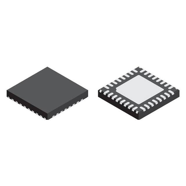
The A89303 is available in a 20-lead TSSOP with exposed
power pad (suffix LP) and a 32-contact 5 mm × 5 mm QFN
with exposed thermal pad and wettable flank (suffix ET).
PACKAGES:
20-lead TSSOP with
exposed thermal pad
(LP package)
32-contact QFN with
exposed thermal pad
and wettable flank
5 mm × 5 mm × 0.90 mm
(ET package)
Not to scale
CP2
CP1
0.22 µF/X7R
Logic Supply
CLK
DATA
OCP
Vds Monitor
Enable
VCP
0.22 µF/X7R
VBB
VBB
Vin
22 µF
I2C serial port
&
EEPROM
System
Variables
Duty In
Charge Pump
VCP
OUTC
GATE
DRIVE
OUTB
OUTA
PWM/SCL
RS
6
FG/SDA
Control
Logic
Ocl
Comp
LSS
LSS
VR
FF1
CTAP
OUTB
OUTC
OUTA
Position
Detect
FF2
GND
Figure 1: Typical Application
A89303-DS
MCO-0000950
August 27, 2020
�A89303
Three-Phase Sensorless Fan Driver IC
SPECIFICATIONS
SELECTION GUIDE
Part Number
Operating Temperature
Range (TA) (°C)
Packaging
Packing
A89303KLPTR-T
–40 to 125
20-lead TSSOP with exposed thermal pad
4000 pieces per 13-inch reel
A89303KETSR-J
–40 to 125
32-contact QFN with exposed thermal pad and wettable flank
6000 pieces per 13-inch reel
ABSOLUTE MAXIMUM RATINGS
Characteristic
Symbol
Notes
Supply Voltage
VBB
Logic Input Voltage Range
VIN
PWM
Logic Output
VO
FG, FF1, FF2
Output Current
IOUT
LSS
VLSS
Output Voltage
VOUT
Rating
Unit
40
V
–0.3 to 6
V
6
V
3.6
A
DC
±0.36
V
t < 200 ns
±2.5
V
–1.5 to VBB + 1
V
CTAP
–0.6 to VBB + 0.6
V
VCP
VBB – 0.3 to VBB + 8
V
CP1
–0.3 to VBB + 0.3
V
CP2
VBB – 0.3 to VCP + 0.3
V
OUTA, OUTB, OUTC
Junction Temperature
TJ
150
°C
Storage Temperature Range
Tstg
–55 to 150
°C
Operating Temperature Range
TA
–40 to 125
°C
THERMAL CHARACTERISTICS
Characteristic
Package Thermal Resistance
Symbol
RθJA
Value
Unit
20-lead TSSOP (package LP), on 2-sided PCB 1-in.2 copper
Test Conditions*
35
°C/W
32-contact QFN (package ET), on 2-sided PCB 1-in.2 copper
40
°C/W
*Additional thermal information available on the Allegro website.
TABLE OF CONTENTS
Features and Benefits............................................................ 1
Description........................................................................... 1
Packages............................................................................. 1
Typical Application................................................................. 1
Specifications....................................................................... 2
Selection Guide................................................................. 2
Absolute Maximum Ratings................................................. 2
Recommended Operational Range...................................... 2
Thermal Characteristics...................................................... 2
Pinout Diagram and Terminal List Table................................... 3
Electrical Characteristics........................................................ 4
Functional Description........................................................... 6
Basic Operation................................................................. 6
TSD/Fault Flag with PWM High Timing................................. 9
Power On / Power Off Timing............................................ 10
Startup Sequence............................................................ 12
PWM Control................................................................... 12
EEPROM Map.................................................................... 13
Serial Port.......................................................................... 14
I2C Timing Diagrams........................................................ 14
Write Command............................................................... 15
Read Command.............................................................. 15
Programming EEPROM.................................................... 16
Application Information........................................................ 18
Pin Diagrams...................................................................... 19
Package Outline Drawings................................................... 20
Allegro MicroSystems
955 Perimeter Road
Manchester, NH 03103-3353 U.S.A.
www.allegromicro.com
2
�A89303
Three-Phase Sensorless Fan Driver IC
PINOUT DIAGRAMS AND TERMINAL LIST TABLE
Terminal List Table
1
20
VCP
CP2
2
19
OUTC
n/c
3
18
VBB
PWM/SCL
4
17
n/c
n/c
5
16
LSS
n/c
6
15
OUTB
FF2
7
14
LSS
FF1
8
13
VBB
FG/SDA
9
12
GND
10
11
n/c
n/c
n/c
n/c
FF2
FF1
n/c
26
27
28
29
30
31
CP2
1
21
Charge pump capacitor
CP1
2
22
Charge pump capacitor
n/c
3
23
4
24
n/c
5
25, 26, 27
OUTA
n/c
6
28, 29, 30
CTAP
FF2
7
31
Logic output signal
FF1
8
32
Logic output signal
n/c
–
1
9
2
n/c
–
3
GND
10
4
n/c
–
5
CTAP
11
6
Motor common
OUTA
12
7
Motor terminal
n/c
–
8
VBB
13
9
CP2
n/c
–
10
20
VCP
LSS
14
11
CTAP
6
19
n/c
OUTA
7
18
OUTC
n/a
8
17
n/c
16
21
5
VBB
4
n/c
15
GND
n/c
CP1
14
22
LSS
3
13
n/c
OUTB
n/c
11
23
12
2
n/c
FG/SDA
LSS
PWM/SCL
9
24
10
1
n/c
Logic input – PWM duty or I2C clock
FG/SDA
n/c
VBB
Description
ET
PWM/SCL
LP Package Pinouts
32
Number
LP
n/c
PAD
Name
25
CP1
ET Package Pinouts
I/O – Speed output signal or I2C data
Ground
Input supply
Low-side source connection
n/c
–
12
OUTB
15
13
Motor terminal
LSS
16
14
Low-side source connection
n/c
17
15
VBB
18
16
n/c
–
17
OUTC
19
18
Input supply
Motor terminal
n/c
–
19
VCP
20
20
Charge pump capacitor
PAD
–
–
Exposed pad for enhanced thermal dissipation
Allegro MicroSystems
955 Perimeter Road
Manchester, NH 03103-3353 U.S.A.
www.allegromicro.com
3
�A89303
Three-Phase Sensorless Fan Driver IC
ELECTRICAL CHARACTERISTICS: Valid for TJ = –40°C to 125°C and VBB = 5.5 to 40 V, unless noted otherwise
Characteristics
Symbol
Test Conditions
Min.
Typ.
Max.
Unit
Driving
5.5
–
VBBOV
V
Operating
5.5
–
40
V
GENERAL
Load Supply Operating Range
VBB
VBB Supply Current
IBB
Charge Pump
VCP
Active mode (PWM duty < DC_ON)
–
8.5
12
mA
6.5
7
7.7
V
Relative to VBB, VBB = 5.5 V
4
5
–
V
IOUT = 1.5 A, TJ = 25°C, VBB = 12 V
–
300
–
mΩ
IOUT = 1.5 A, TJ = 125°C, VBB = 12 V
–
450
520
mΩ
Source Driver, TJ = 25°C, VBB = 12 V
–
150
–
mΩ
Relative to VBB, VBB = 8 V
POWER DRIVER
Total Driver On-Resistance
(Sink + Source)
RDS(ON)
–
150
–
mΩ
fPWM
Sink Driver, TJ = 25°C, VBB = 12 V
23.3
24.5
25.7
kHz
fPWMIN
2.1
–
45
kHz
Duty Cycle On Threshold
DCON
9.5
10
10.5
%
Duty Cycle Off Threshold
DCOFF
7
7.5
8
%
External PWM Delay ON
tPWM_ON
494
520
546
μs
External PWM Delay OFF
tPWM_OFF
494
520
546
μs
Motor PWM Frequency
MOTOR CONTROL LOGIC
PWM Input Frequency Range
PROTECTION CIRCUITS
VBB Undervoltage Threshold
VBBUVLO
VBB Undervoltage Hysteresis
VBBHYS
VBB Overvoltage
VBB Overvoltage Hysteresis
VBBOV
VBB rising
VBB rising
VBBOVHYS
4.85
5
V
500
600
mV
29
–
31.5
V
1.5
2
2.5
V
VCP UVLO
VCPUVLO
3.6
3.85
4.1
V
VCP UVLO Hysteresis [2]
VCPUVHYS
200
–
400
mV
tVCPUV
–
80
400
μs
tPOR_DELAY
–
80
90
μs
–5
0
5
%
5
–
–
A
Charge Pump Power Up Time [2]
POR Delay Time
VCP rising
4.7
400
Overcurrent Threshold
VOCL
Overcurrent Protection
IOCP
Thermal Shutdown Temperature
TJTSD
Temperature increasing
165
175
185
°C
ΔTJ
Recovery = TJTSD – ΔTJ
–
20
–
°C
Thermal Shutdown Hysteresis
[1]
[2]
VRI = 160 mV
Specified limits are tested at a single temperature and assured over temperature range by design and characterization.
Ensured by design and characterization, not production tested
Continued on next page...
Allegro MicroSystems
955 Perimeter Road
Manchester, NH 03103-3353 U.S.A.
www.allegromicro.com
4
�A89303
Three-Phase Sensorless Fan Driver IC
ELECTRICAL CHARACTERISTICS (continued): Valid for TJ = –40°C to 125°C and VBB = 5.5 to 40 V, unless noted otherwise
Characteristics
Symbol
Test Conditions
Min.
Typ.
Max.
Unit
–5
0
很抱歉,暂时无法提供与“A89303KETSR-J”相匹配的价格&库存,您可以联系我们找货
免费人工找货