APS12400
Two-Wire Hall-Effect Latch
FEATURES AND BENEFITS
• ASIL A functional safety
□□ Developed in accordance with ISO 26262:2011
(pending assessment)
□□ Internal diagnostics and a defined Safe State
□□ A2-SIL™ documentation available
• Multiple product options
□□ Magnetic polarity, switch points, and hysteresis
□□ Temperature coefficient (supports SmCo, NdFeB, and
ferrite magnets)
□□ Output polarity and current levels
• Reduces module bill of materials (BOM) and assembly cost
□□ Integrated overvoltage clamp (40 V load dump) and
reverse-battery diode
□□ Integrated series resistor and bypass capacitor (UC package)
□□ Enables PCB-less sensor modules
• Automotive-grade ruggedness and fault tolerance
□□ Extended AEC-Q100 Grade 0 qualification
□□ Operation at –40°C to 175°C junction temperature
□□ 3 to 24 V operating voltage range
□□ High EMC/ESD immunity
□□ Overtemperature indication
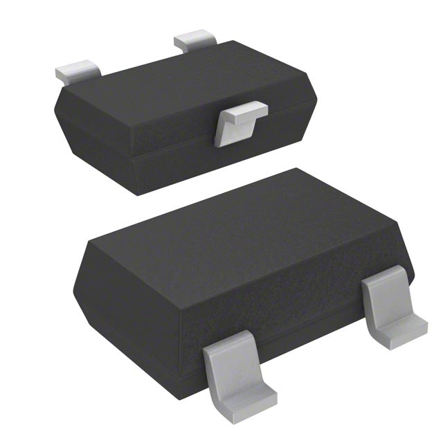
PACKAGES
3-pin SOT23-W (LH)
DESCRIPTION
APS12400 devices are two-wire planar Hall-effect sensor
integrated circuits (ICs) developed in accordance with
ISO 26262:2011 (pending assessment). They include internal
diagnostics and support a functional safety level of ASIL A.
The enhanced two-wire current-mode interface provides
interconnect open/short diagnostics and adds a Safe State
to communicate diagnostic information while maintaining
compatibility with legacy two-wire systems. Two-wire sensors
are well-suited to safety applications, especially those involving
long wire harnesses.
The APS12400 is a factory-calibrated latch (bipolar switch)
available in several product options including magnetic
switch points, temperature coefficient, and output polarity.
The response can be matched to SmCo, NdFeB, or low-cost
ferrite magnets. There is a choice of two output current levels
and either output polarity.
APS12400 sensors are engineered to operate in the harshest
environments with minimal external components. They are
qualified beyond the requirements of AEC-Q100 Grade 0
and will survive extended operation at 175°C junction
Continued on the next page…
3-pin ultramini SIP (UA)
3-pin SIP (UC)
TYPICAL APPLICATIONS
• Automotive and industrial safety systems
• Sunroof/convertible top/tailgate/liftgate actuation
• Clutch-by-wire
• Electric power steering (EPS)
• Transmissions actuators
• Wiper motors
Not to scale
VCC
VINT
68 Ω
0.1 µF
Regulator
UVLO
Device
Configuration
ICC Adjust
0.01 µF
Clock Generator
UC Package
Only
Dynamic Offset
Cancellation
LH and UA
Packages
Only
Switch Point
Control
Output
Polarity
Amp
Low-Pass
Filter
Functional Block Diagram
APS12400-DS, Rev. 3
MCO-0000402
Temp
Comp
GND
April 3, 2020
�APS12400
Two-Wire Hall-Effect Latch
DESCRIPTION (continued)
temperature. These monolithic ICs include on-chip reverse-battery
protection, overvoltage protection (40 V load dump), ESD protection,
overtemperature detection, and an internal voltage regulator for
operation directly from an automotive battery bus. These integrated
features reduce the end-product bill of materials (BOM) and
assembly cost.
The available SIP package with integrated discrete components
(UC) enables PCB-less applications by incorporating all of the EMC
protection components into the IC package. Other package options
include industry-standard surface-mount SOT (LH) and throughhole SIP (UA) packages. All three packages are RoHS-compliant
and lead (Pb) free with 100% matte-tin-plated leadframes.
For situations where a functionally equivalent but factory-programmed
two-wire latch or end-of-line programmable device is preferred, refer
to the APS12400 and APS11900 device families, respectively.
RoHS
COMPLIANT
Complete Part Number Format
Allegro Iden�fier (Device Family)
APS – Digital Posi�on Sensor
Configura�on Op�ons
APS 12400
Allegro Device Number
12400 – 2-wire Planar Hall-effect Latch
LLHALX- 0L1A
Temperature Coefficient
A – Flat
B – -0.035%/°C
C – -0.12%/°C
D – -0.2%/°C
ICC(L) Selec�on
1 – 5 to 6.9 mA
2 – 2 to 5 mA
Output Polarity for B > BOP
H – ICC(H)
L – ICC(L)
Device Switch Threshold
0 – BOP: +80 G max; BRP: -80 G max
1 – BOP: +40 G max; BRP: -40 G max
Instruc�ons (Packing)
LT – 7-in. reel, 3,000 pieces/reel (LH Only)
LX – 13-in. reel, 10,000 pieces/reel (LH Only)
TN – 13-in . reel , 4,000 pieces /reel (UA Only )
(no op�on code) – bulk, 500 pieces/bag (UA Only)
Package Designa�on
LHA – 3-pin SOT23W Surface Mount
UAA – 3-pin SIP Through-Hole
UCD* – 3-pin SIP Through-Hole w/ passives
Ambient Opera�ng Temperature Range
L – -40°C to +150°C
* Contact Allegro for availability.
Allegro MicroSystems
955 Perimeter Road
Manchester, NH 03103-3353 U.S.A.
www.allegromicro.com
2
�APS12400
Two-Wire Hall-Effect Latch
SELECTION GUIDE
Part Number [1]
Package
Packing
APS12400LLHALT-0H1A
3-pin SOT23-W surface mount
7-inch reel, 3000 pieces/reel
APS12400LLHALX-0H1A
3-pin SOT23-W surface mount
13-inch reel, 10000 pieces/reel
APS12400LUAA-0H1A
3-pin SIP through-hole
Bulk, 500 pieces/bag
APS12400LUAATN-0H1A
3-pin SIP through-hole
13-inch reel, 4000 pieces/reel
APS12400LUAA-0H2A
3-pin SIP through-hole
Bulk, 500 pieces/bag
APS12400LUAATN-0H2A
3-pin SIP through-hole
13-inch reel, 4000 pieces/reel
APS12400LUCD-0H1A [2]
3-pin SIP through-hole
Bulk, 500 pieces/bag
APS12400LUCDTN-0H1A [2]
3-pin SIP through-hole
13-inch reel, 4000 pieces/reel
[1] Contact Allegro
[2] Contact Allegro
Magnetic
Temperature
Coefficient
Output Polarity
for B > BOP
Device Switch
Threshold (G)
ICC(L)
Selection
(mA)
Flat
ICC(H)
BOP: +80 max
BRP: –80 max
5 to 6.9
Flat
ICC(H)
BOP: +80 max
BRP: –80 max
5 to 6.9
Flat
ICC(H)
BOP: +80 max
BRP: –80 max
2 to 5
Flat
ICC(H)
BOP: +80 max
BRP: –80 max
5 to 6.9
MicroSystems for options not listed in the selection guide.
MicroSystems for availability.
Allegro MicroSystems
955 Perimeter Road
Manchester, NH 03103-3353 U.S.A.
www.allegromicro.com
3
�APS12400
Two-Wire Hall-Effect Latch
SPECIFICATIONS
ABSOLUTE MAXIMUM RATINGS
Characteristic
Supply
Symbol
Notes
Rating
Unit
VCC
40
V
VRCC
–23
V
Voltage [1]
Reverse Supply Voltage
B
Unlimited
G
165
°C
175
°C
–65 to 170
°C
Magnetic Flux Density
Maximum Junction Temperature
TJ(max)
Storage Temperature
For 500 hours
Tstg
[1] This
rating does not apply to extremely short voltage transients such as load dump and/or ESD. Those events have individual ratings
specific to the respective transient voltage event. Contact your local field applications engineer for information on EMC test results.
INTERNAL DISCRETE COMPONENT RATINGS (UC Package Only)
Characteristics
Component
Symbol
Test Conditions
Resistor
RSERIES
In series with VCC
Capacitor
CSUPPLY
Connected between VCC and GND
Rated Nominal
Rated
Resistance/Capacitance Voltage
Rated
Tolerance
Rated Temp.
Range
Rated Power
Handling
68 Ω
50 V
±15%
–
1/8 W
100 nF
50 V
±10%
X7R
–
Allegro MicroSystems
955 Perimeter Road
Manchester, NH 03103-3353 U.S.A.
www.allegromicro.com
4
�APS12400
Two-Wire Hall-Effect Latch
PINOUT DIAGRAMS AND TERMINAL LIST TABLE
3
Terminal List Table (LH, UA Packages)
Number
Package Name
Function
LH
UA
1
VCC
VCC
Supply voltage
2
GND
GND
Ground terminal
3
GND
GND
Ground terminal
Note: For best performance, tie Pins 2 and 3 together
close to the IC.
2
1
1
LH Package, 3-Pin SOT23W Pinout
2
3
UA Package, 3-Pin SIP Pinout
Terminal List Table (UC Package)
Number
1
2
3
Package Name
UC
Function
VCC
Supply voltage
VINT
This pin reflects the internal
voltage, VINT, after the
internal series resistor. This
pin should be kept floating.
GND
100 nF
68 Ω
Ground terminal
1
2
3
UC Package, 3-Pin SIP Pinout
Allegro MicroSystems
955 Perimeter Road
Manchester, NH 03103-3353 U.S.A.
www.allegromicro.com
5
�APS12400
Two-Wire Hall-Effect Latch
ELECTRICAL CHARACTERISTICS: Valid over full operating voltage and ambient temperature ranges for TJ < TJ(max) and
CBYP = 0.01 µF, unless otherwise specified
Characteristics
Symbol
Test Conditions
Min.
Typ. [3]
Max.
Unit
SUPPLY AND STARTUP
Supply Voltage
Operating, TJ < 165°C
LH and UA
packages
3.0
–
24
V
Operating, TJ < 165°C
UC package
4.33
–
24
V
VCC(UV)DIS
After power-on, as VCC increases, output
is forced to POS until this voltage is
reached
LH and UA
packages
–
2.6
–
V
UC package
–
3.5
–
V
VCC(UV)EN
After POK, when VCC drops below this
voltage, output is forced to POS
LH and UA
packages
–
2.3
–
V
UC package
–
3.2
–
V
ICC(L1)
5
–
6.9
mA
ICC(L2)
2
–
5
mA
VCC
Undervoltage Lockout [4]
Supply Current
ICC(H)
ISAFE
Output Slew Rate
dI/dt
12
–
17
mA
Safe current state. Indicates overtemperature or device
configuration error.
–
–
2
mA
No bypass capacitor; CL [5] = 20 pF
LH and UA
packages
–
50
–
mA/µs
–
0.22
–
mA/µs
UC package
–
0.22
–
mA/µs
–
70
CBYP = 100 nF; CL [5] = 20 pF
Internal bypass capacitor; CL [5] = 20 pF
Power-On Time
[6]
Power-On State [7]
Chopping Frequency
tPO
POS
VCC ≥ VCC(min), B > BOP(max), B < BRP(min)
fC
Output Jitter (p-p)
–
t < tPO, VCC ≥ VCC(UV)EN
µs
ICC(H)
mA
–
800
–
kHz
1 kHz square wave signal
–
5
–
µs
ON-BOARD PROTECTION
Supply Zener Clamp Voltage
VZ
ICC = ICC(H) + 1 mA, TA = 25°C
40
–
–
V
Reverse Supply Zener Clamp
Voltage
VRZ
ICC = –1 mA
–
–
–23
V
Overtemperature Shutdown
TSD
Temperature increasing
–
205
–
°C
Overtemperature Hysteresis
TJHYS
–
25
–
°C
Typical data is at TA = 25°C and VCC = 12 V unless otherwise noted; for design information only.
UC minimum VCC is higher to accommodate voltage drop in the internal series resistor. UC package minimum VCC is higher to accommodate
voltage drop in the internal series resistor. This also affects the VCC(UV).
[5] C – scope capacitance.
L
[6] Measured from V
CC ≥ VCC(MIN) to valid output.
[7] Power-on state is defined only when V
CC slew rate 1 V/s or greater
[3]
[4]
Allegro MicroSystems
955 Perimeter Road
Manchester, NH 03103-3353 U.S.A.
www.allegromicro.com
6
�APS12400
Two-Wire Hall-Effect Latch
MAGNETIC CHARACTERISTICS: Valid over full operating voltage and ambient temperature ranges for TJ < TJ(max) and
CBYP = 0.01 µF, unless otherwise specified
Characteristics
Operate Point
Release Point
Hysteresis
Switch Point Temperature
Coefficient
[8]
[9]
Symbol
BOP
BRP
BHYS
Magnetic
Switch Point
Option
Temperature
Coefficient
Test Conditions
Min.
Typ. [8]
Max.
Unit [9]
5
–
80
G
-0
A – Flat
TA = –40°C to 150°C
-1
A – Flat
TA = –40°C to 150°C
5
–
40
G
-0
A – Flat
TA = –40°C to 150°C
–80
–
–5
G
-1
A – Flat
TA = –40°C to 150°C
–40
–
–5
G
-0
A – Flat
TA = –40°C to 150°C
40
–
110
G
-1
A – Flat
TA = –40°C to 150°C
15
40
65
G
All
A – Flat
TA = –40°C to 150°C
–
0
–
%/°C
Typical data is at TA = 25°C and VCC = 12 V, unless otherwise noted; for design information only.
Magnetic flux density, B, is indicated as a negative value for north-polarity magnetic fields, and a positive value for south-polarity magnetic fields.
Allegro MicroSystems
955 Perimeter Road
Manchester, NH 03103-3353 U.S.A.
www.allegromicro.com
7
�APS12400
Two-Wire Hall-Effect Latch
THERMAL CHARACTERISTICS: May require derating at maximum conditions; see application information
Characteristic
Symbol
Test Conditions*
RθJA
Package Thermal Resistance
Value
Unit
Package LH, on 1-layer PCB based on JEDEC standard
228
°C/W
Package LH, on 2-layer PCB with 0.463 in.2 of copper area each side
110
°C/W
Package UA, on 1-layer PCB with copper limited to solder pads
165
°C/W
Package UC, on 1-layer PCB with copper limited to solder pads
270
°C/W
*Additional thermal information available on the Allegro website.
Maximum Allowable VCC (V)
Power Derating Curve
28
27
26
25
24
23
22
21
20
19
18
17
16
15
14
13
12
11
10
9
8
7
6
5
4
3
2
VCC(max)
2-layer PCB, LH package
(RθJA = 110 °C/W)
1-layer PCB, Package UC
(RθJA = 270°C/W)
1-layer PCB, UA package
(RθJA = 165 °C/W)
1-layer PCB, LH package
(RθJA = 228°C/W)
20
40
60
80
100
VCC(min)
120
140
160
180
Ambient Temperature (°C)
Power Dissipation, PD (mW)
Power Dissipation versus Ambient Temperature
1900
1800
1700
1600
1500
1400
1300
1200
1100
1000
900
800
700
600
500
400
300
200
100
0
Package LH, 2-layer PCB
(RθJA = 110°C/W)
Package UA, 1-layer PCB
(RθJA = 165°C/W)
Package LH, 1-layer PCB
(RθJA = 228°C/W)
Package UC, 1-layer PCB
(RθJA = 270°C/W)
20
40
60
80
100
120
140
160
180
Temperature (°C)
Allegro MicroSystems
955 Perimeter Road
Manchester, NH 03103-3353 U.S.A.
www.allegromicro.com
8
�APS12400
Two-Wire Hall-Effect Latch
CHARACTERISTIC PERFORMANCE DATA
ICC(H) vs. TA
ICC(H) vs. VCC
17
16
VCC (V)
15
3
12
14
15
13
24
12
-50
-20
10
40
70
100
130
Supply Current, ICC(H) (mA)
Supply Current, ICC(H) (mA)
17
16
TA (°C)
15
-40
14
25
150
13
12
160
0
5
10
Ambient Temperature, TA (°C)
ICC(L1) vs. TA
6.5
VCC (V)
6.25
3
6
12
5.75
15
5.5
24
5.25
-20
10
40
70
100
130
Supply Current, ICC(L1) (mA)
Supply Current, ICC(L1) (mA)
6.75
-50
160
7
6.8
6.6
6.4
6.2
6
5.8
5.6
5.4
5.2
5
-40
25
150
0
5
10
ICC(L2) vs. TA
15
20
25
30
ICC(L2) vs. VCC
5
4.5
VCC (V)
4
3
3.5
12
3
15
2.5
24
-50
-20
10
40
70
100
130
Supply Current, ICC(L2) (mA)
Supply Current, ICC(L2) (mA)
30
Supply Voltage, VCC (V)
5
4.5
-40
3.5
25
3
150
2.5
2
160
TA (°C)
4
0
5
Ambient Temperature, TA (°C)
10
ISAFE vs. TA
20
25
30
ISAFE vs. VCC
1.5
VCC (V)
1.25
1
3
0.75
24
0.5
0.25
-50
-20
10
40
70
100
Ambient Temperature, TA (°C)
130
160
Supply Current, ISAFE (mA)
2
1.75
0
15
Supply Voltage, VCC (V)
2
Supply Current, ISAFE (mA)
25
TA (°C)
Ambient Temperature, TA (°C)
2
20
ICC(L1) vs. VCC
7
5
15
Supply Voltage, VCC (V)
1.75
1.5
TA (°C)
1.25
-40
1
0.75
25
0.5
150
0.25
0
0
5
10
15
20
25
30
Supply Voltage, VCC (V)
Allegro MicroSystems
955 Perimeter Road
Manchester, NH 03103-3353 U.S.A.
www.allegromicro.com
9
�APS12400
Two-Wire Hall-Effect Latch
FUNCTIONAL DESCRIPTION
Functional Safety
Operation
The APS12400 was designed in accordance with the international
standard for automotive functional safety,
ISO 26262:2011 (pending assessment). This
2
product achieves an ASIL (Automotive Safety
Integrity Level) rating of ASIL A according to
the standard. The APS12400 is classified as a
SEooC (Safety Element out of Context) and
can be easily integrated into safety-critical systems requiring
higher ASIL ratings that incorporate external diagnostics or use
measures such as redundancy. Safety documentation will be
provided to support and guide the integration process. Contact
your local FAE for A2-SIL™ documentation: www.allegromicro.
com/ASIL.
The APS12400 devices are two-wire unipolar planar Hall-effect
latches. The user can select a device that respond to a north or
south magnetic field. There is a choice of two output current
levels, ICC(L1) and ICC(L2), and the user can determine which current state is applied, ICC(L) or ICC(H), when the magnetic field is
greater than BOP or less than BRP.
-
The APS12400 has internal diagnostics to check the voltage supply
(an undervoltage lockout regulator) and to detect overtemperature
conditions. See the Diagnostics section for more information.
The difference between the magnetic operate and release points is
called the hysteresis of the device, BHYS. Hysteresis allows clean
switching of the output even in the presence of external mechanical vibration and electrical noise.
Figure 1 shows the potential configuration options for the
APS12400. The direction of the applied magnetic field is perpendicular to the branded face for the APS12400. See Figure 2 for an
illustration.
Latch
I+
ICC(H)
Switch to Low
Switch to High
Standard
Output
Polarity
(POL = 0)
BRP
0
BOP
ICC(L)
0
B+
A
Y
X
B
Y
X
C
Y
X
BHYS
Z
Z
Latch
I+
Switch to High
ICC(H)
Switch to Low
Reversed
Output
Polarity
(POL = 1)
Z
Figure 2: Magnetic Sensing Orientations
APS12400 LH (Panel A), UA (Panel B), and UC (Panel C)
BRP
0
BOP
ICC(L)
0
B+
BHYS
Figure 1: Unipolar Hall Latch Magnetic and
Output Current Polarity Options
B- indicates increasing north polarity magnetic field strength, and
B+ indicates increasing south polarity magnetic field strength.
Allegro MicroSystems
955 Perimeter Road
Manchester, NH 03103-3353 U.S.A.
www.allegromicro.com
10
�APS12400
Two-Wire Hall-Effect Latch
Power-On Behavior
The APS12400 has an internal voltage regulator with undervoltage lockout. As the device powers up, it stays in the power-on
state (POS) of ICC(H) until the supply voltage exceeds VCC(UV)DIS.
After tPO, the current consumption is ICC(L) or ICC(H), according
to the magnetic field and the device configuration, as shown in
Figure 1.
Similarly, when the supply voltage decreases, the device returns
to the power on state (POS) when the supply voltage drops below
VCC(UV)EN, as shown in Figure 3.
When the device powers on in the hysteresis range (less than BOP
and higher than BRP), the output corresponds to the power-on
state. In this case, the correct state is attained after the first excursion beyond BOP or BRP.
Any value of ICC between the allowed ranges for ICC(H) and ICC(L)
indicates a general fault condition.
+ mA
ICC(H) (max)
ICC(H) (min)
ICC(L) (max)
ICC(L) (min)
Fault
ICC(H) Range
Fault
ICC(L) Range
Fault
ISAFE
0
Overtemp, Device Config Error ISAFE Range
Fault
Figure 4: Interpreting ICC for System-Level Diagnostics
Key
VCC for LH, UA;
VINT for UC
V
POS
Temperature Coefficient and Magnet Selection
VCC(min)
VCC(UV)DIS
VCC(UV)EN
V
0
POS
ICC
ICC(H)
Current Undefined
tPO
Output according to
device se�ngs, based
on B
t
POS
Current
Undefined
ICC(Lx)
t
Figure 3: Power-On/UVLO Behavior
Diagnostic Features
When properly supplied, APS12400 always has current flowing at
a specified level: either ICC(H), ICC(L ), or ISAFE. Any current outside of these narrow ranges is a fault condition. If there is a short,
current increases so that ICC > ICC(H) (max), outside the valid ICC(H)
range. If there is an open, the current lowers below the ICC(L) (min),
outside the valid output current range. In this way, connectivity
issues between the ECU and the sensor can easily be detected.
Additionally, the APS12400 has an overtemperature feature: if
the junction temperature increases beyond TSD, then the current
is reduced to ISAFE. The device current also changes to ISAFE if
there is an error in the device configuration which is checked at
power-on and after an overtemperature event.
The APS12400 allows the user to select the magnetic temperature coefficient to compensate for drifts of SmCo, NdFeB, and
ferrite magnets over temperature—as indicated in the specifications table on page 5. This compensation improves the magnetic
system performance over the entire temperature range. For
example, the magnetic field strength from ferrite decreases as the
temperature increases from 25°C to 150°C. This lower magnetic
field strength means that a lower switching threshold is required
to maintain switching at the same distance from the magnet to the
sensor. Correspondingly, higher switching thresholds are required
at cold temperatures, as low as –40°C, due to the higher magnetic
field strength from the ferrite magnet. The APS12400 compensates the switching thresholds over temperature as described
above. It is recommended that system designers evaluate their
magnetic circuit over the expected operating temperature range to
ensure the magnetic switching requirements are met.
For example, the typical ferrite compensation is –0.2%/°C.
With a 25°C temperature BOP switch point of 80 G, the switch
point changes nominally by –0.2%/°C × 80 × (150°C – 25°C) =
–20 G to 80 G – 20 G = 60 G at 150°C. And at –40°C, the switch
point changes by –0.2%/°C × 80 × (–40°C – 25°C) = 10 G to
80 G + 10 G = 90 G.
Allegro MicroSystems
955 Perimeter Road
Manchester, NH 03103-3353 U.S.A.
www.allegromicro.com
11
�APS12400
Two-Wire Hall-Effect Latch
Applications
For the LH and UA packages, an external bypass capacitor (from
0.01 µF to 0.1 µF) should be connected (in close proximity to
the Hall element) between the supply and ground of the device
to reduce both external noise and noise generated by the chopper stabilization. Some applications may require additional EMC
immunity which is achieved with an enhanced protection circuit.
For example, increasing the bypass capacitor from 0.01 µF to
0.1 µF improves immunity to Powered ESD (ISO 10605) and
Direct Capacitive Coupling.
A series resistor and a 0.1 µF bypass capacitor is integrated into
the UC package, making it easy to achieve an EMC-robust design
with no external components or PCB required.
Note that the bypass capacitor selection directly affects the slew
rate. See the Electrical Characteristics table for the typical slew
rate with 0.1 µF bypass capacitor. A 0.01 µF bypass capacitor
slew rate is ten times faster.
Typical application circuits are shown in “Figure 5: Typical
Application Circuits” on page 13.
Extensive applications information for Hall-effect devices is
available in:
• Hall-Effect IC Applications Guide, AN27701
• Hall-Effect Devices: Guidelines For Designing Subassemblies
Using Hall-Effect Devices, AN27703.1
• Soldering Methods for Allegro’s Products – SMT and ThroughHole, AN26009
• www.allegromicro.com/ASIL
All are provided on the Allegro Web site:
www.allegromicro.com
Allegro MicroSystems
955 Perimeter Road
Manchester, NH 03103-3353 U.S.A.
www.allegromicro.com
12
�APS12400
Two-Wire Hall-Effect Latch
V+
ECU
VCC
APS12400
R SENSE
V SENSE
V+
C BYP
0.1 µF
VCC
C BYP
0.1 µF
A119x
APS12400
GND
V SENSE
ECU
R SENSE
GND
(A) Low-Side Sensing (LH, UA package)
(B) High-Side Sensing (LH, UA package)
ECU
VCC
V+
R SENSE
APS12400
V SENSE
68 Ω
V+
VINT
VCC
APS12400
68 Ω
0.1 µF
VINT
GND
ECU
0.1 µF
V SENSE
R SENSE
GND
(C) Low-Side Sensing (UC package)
(D) High-Side Sensing (UC package)
Figure 5: Typical Application Circuits
Allegro MicroSystems
955 Perimeter Road
Manchester, NH 03103-3353 U.S.A.
www.allegromicro.com
13
�APS12400
Two-Wire Hall-Effect Latch
Chopper Stabilization Technique
A limiting factor for switch point accuracy when using Halleffect technology is the small-signal voltage developed across
the Hall plate. This voltage is proportionally small relative to the
offset that can be produced at the output of the Hall sensor. This
makes it difficult to process the signal and maintain an accurate,
reliable output over the specified temperature and voltage range.
Chopper stabilization is a proven approach used to minimize
Hall offset.
The technique, dynamic quadrature offset cancellation, removes
key sources of the output drift induced by temperature and package stress. This offset reduction technique is based on a signal
modulation-demodulation process. “Figure 6: Model of Chopper
Stabilization Circuit (Dynamic Offset Cancellation)” illustrates
how it is implemented.
The undesired offset signal is separated from the magnetically
induced signal in the frequency domain through modulation. The
subsequent demodulation acts as a modulation process for the
offset causing the magnetically induced signal to recover its original spectrum at baseband while the DC offset becomes a highfrequency signal. Then, using a low-pass filter, the signal passes
while the modulated DC offset is suppressed. Allegro’s innovative
chopper-stabilization technique uses a high-frequency clock.
The high-frequency operation allows a greater sampling rate that
produces higher accuracy, reduced jitter, and faster signal processing. Additionally, filtering is more effective and results in a
lower noise analog signal at the sensor output. Devices such as the
APS12400 that use this approach have an extremely stable quiescent Hall output voltage, are immune to thermal stress, and have
precise recoverability after temperature cycling. This technique is
made possible through the use of a BiCMOS process which allows
the use of low offset and low noise amplifiers in combination with
high-density logic and sample-and-hold circuits.
Regulator
Hall Element
Amp
Sample and
Hold
Clock/Logic
Low-Pass
Filter
Figure 6: Model of Chopper Stabilization Circuit
(Dynamic Offset Cancellation)
Allegro MicroSystems
955 Perimeter Road
Manchester, NH 03103-3353 U.S.A.
www.allegromicro.com
14
�APS12400
Two-Wire Hall-Effect Latch
POWER DERATING
The device must be operated below the maximum junction
temperature, TJ (max). Reliable operation may require derating
supplied power and/or improving the heat dissipation properties
of the application.
17 mA, calculate the maximum allowable power level, PD (max).
First, using equation 3:
∆T (max) = TJ (max) – TA = 165°C – 150°C = 15°C
Thermal Resistance (junction to ambient), RθJA, is a figure of
merit summarizing the ability of the application and the device to
dissipate heat from the junction (die), through all paths to ambient air. RθJA is dominated by the Effective Thermal Conductivity,
K, of the printed circuit board which includes adjacent devices
and board layout. Thermal resistance from the die junction to
case, RθJC, is a relatively small component of RθJA. Ambient air
temperature, TA, and air motion are significant external factors in
determining a reliable thermal operating point.
This provides the allowable increase to TJ resulting from internal
power dissipation. Then, from equation 2:
The following three equations can be used to determine operation
points for given power and thermal conditions.
PD (max) = ∆T (max) ÷ RθJA = 15°C ÷ 165°C/W = 91 mW
Finally, using equation 1, solve for maximum allowable VCC for
the given conditions:
VCC (est) = PD (max) ÷ ICC (max) = 91 mW ÷ 17 mA = 5.4 V
The result indicates that, at TA, the application and device can
dissipate adequate amounts of heat at voltages ≤ VCC (est).
PD = VIN × IIN
(1)
If the application requires VCC > VCC(est) then RθJA must by
improved. This can be accomplished by adjusting the layout,
PCB materials, or by controlling the ambient temperature.
∆T = PD × RθJA
(2)
Determining Maximum TA
TJ = TA + ∆T
(3)
In cases where the VCC (max) level is known, and the system
designer would like to determine the maximum allowable ambient temperature TA (max), for example, in a worst-case scenario
with conditions VCC (max) = 24 V, ICC (max) = 17 mA, and RθJA
= 228°C/W for the LH package using equation 1, the largest possible amount of dissipated power is:
For example, given common conditions: TA = 25°C, VCC = 12 V,
ICC = 6 mA, and RθJA = 110°C/W for the LH package, then:
PD = VCC × ICC = 12 V × 6 mA = 72 mW
∆T = PD × RθJA = 72 mW × 110°C/W = 7.92°C
TJ = TA + ∆T = 25°C + 7.92°C = 32.92°C
Determining Maximum VCC
For a given ambient temperature, TA, the maximum allowable power dissipation as a function of VCC can be calculated.
PD (max) represents the maximum allowable power level without
exceeding TJ (max) at a selected RθJA and TA.
Example: VCC at TA = 150°C, package UA, using low-K PCB.
Using the worst-case ratings for the device, specifically: RθJA =
165°C/W, TJ (max) = 165°C, VCC (max) = 24 V, and ICC (max) =
PD = VIN × IIN
PD = 24 V × 17 mA = 408 mW
Then, by rearranging equation 3 and substituting with equation 2:
TA (max) = TJ (max) – ΔT
TA (max) = 165°C – (408 mW × 228°C/W)
TA (max) = 165°C – 93°C = 72°C
Finally, note that the TA (max) rating of the device is 150°C and
performance is not guaranteed above this temperature for any
power level.
Allegro MicroSystems
955 Perimeter Road
Manchester, NH 03103-3353 U.S.A.
www.allegromicro.com
15
�APS12400
Two-Wire Hall-Effect Latch
Package LH, 3-Pin SOT23W
+0.12
2.98 –0.08
1.49 D
4°±4°
3
A
+0.020
0.180–0.053
0.96 D
+0.10
2.90 –0.20
+0.19
1.91 –0.06
2.40
0.70
D
0.25 MIN
1.00
2
1
0.55 REF
0.25 BSC
0.95
Seating Plane
Gauge Plane
8× 10° REF
B
PCB Layout Reference View
Branded Face
1.00 ±0.13
0.95 BSC
+0.10
0.05 –0.05
0.40 ±0.10
XXX
1
C
Standard Branding Reference View
Line 1 = Three digit assigned brand number
For reference only; not for tooling use (reference DWG-0000055).
Dimensions in millimeters.
Dimensions exclusive of mold flash, gate burrs, and dambar protrusions.
Exact case and lead configuration at supplier discretion within limits shown.
A
Active Area Depth, 0.28 ±0.04 mm
B
Reference land pattern layout
All pads a minimum of 0.20 mm from all adjacent pads; adjust as necessary
to meet application process requirements and PCB layout tolerances
C
Branding scale and appearance at supplier discretion
D
Hall element, not to scale
Allegro MicroSystems
955 Perimeter Road
Manchester, NH 03103-3353 U.S.A.
www.allegromicro.com
16
�APS12400
Two-Wire Hall-Effect Latch
Package UA, 3-Pin SIP
+0.08
4.09 –0.05
45°
B
C
E
+0.08
3.02 –0.05
2.05 NOM
1.52 ±0.05
1.44 NOM
E
10°
Mold Ejector
Pin Indent
E
Branded
Face
A
1.02
MAX
45°
XXX
0.79 REF
1
D Standard Branding Reference View
1
2
Line 1: Logo A
Line 2: Three digit assigned brand number
3
+0.03
0.41 –0.06
14.99 ±0.25
+0.05
0.43 –0.07
For reference only; not for tooling use (reference DWG-0000404, Rev. 1).
Dimensions in millimeters.
Dimensions exclusive of mold flash, gate burrs, and dambar protrusions.
Exact case and lead configuration at supplier discretion within limits shown.
A
Dambar removal protrusion (6×)
B
Gate and tie bar burr area
C
Active Area Depth, 0.50 ±0.08 mm
D
Branding scale and appearance at supplier discretion
E
Hall element (not to scale)
1.27 NOM
Allegro MicroSystems
955 Perimeter Road
Manchester, NH 03103-3353 U.S.A.
www.allegromicro.com
17
�APS12400
Two-Wire Hall-Effect Latch
Package UC, 3-Pin SIP
For Reference Only – Not for Tooling Use
(Reference DWG-0000409, Rev. 3)
Dimensions in millimeters – NOT TO SCALE
Dimensions exclusive of mold flash, gate burs, and dambar protrusions
Exact case and lead configuration at supplier discretion within limits shown
0.545 REF× 2
B
1.36 REF
+0.05
0.10
–0.10
4×10°
+0.06
4.00
–0.05
1.50 ±0.05
Detail A
C
R 0.20 All Corners
0.25 REF × 4
Detail A
1.5
4.00
0.15 REF
Mold Ejector
Pin Indent
+0.06
–0.07
E
Branded
Face
45°
A
0.25 REF
0.42 ±0.05
0.30 REF
XXXXX
Date Code
Lot Number
0.85 ±0.05
1.27 REF × 2
D Standard Branding Reference View
1
18.00 ±0.10
2
3
Lines 1, 2, 3: max. 5 characters per line
12.20 ±0.10
0.25
+0.07
–0.03
Line 1: 5-digit Part Number
Line 2: 4-digit Date Code
Line 3: Characters 5, 6, 7, 8 of
Assembly Lot Number
Plating Included
0.38 REF
A Dambar removal protrusion (12×)
0.25 REF
B
0.85 ±0.05
1.80
Gate and tie burr area
C Active Area Depth, 0.38 ±0.05 mm
D Branding scale and appearance at supplier discretion
+0.06
–0.07
F
4.00 +0.06
–0.05
E
Hall element (not to scale)
F
Molded Lead Bar to prevent damage to leads during shipment
R 0.30 All Corners
1.50 ±0.05
Allegro MicroSystems
955 Perimeter Road
Manchester, NH 03103-3353 U.S.A.
www.allegromicro.com
18
�APS12400
Two-Wire Hall-Effect Latch
REVISION HISTORY
Number
Date
Description
–
March 23, 2018
Initial release
1
September 11, 2018
2
April 1, 2019
Updated ASIL status (page 1 and 10)
3
April 3, 2020
Minor editorial updates
Updated Selection Guide table (page 3), Corrected supply current values and plots (pages 6 and 9);
added UC package availability footnote to Complete Part Number Format diagram and Selection Guide
table (page 2-3)
Copyright 2020, Allegro MicroSystems.
Allegro MicroSystems reserves the right to make, from time to time, such departures from the detail specifications as may be required to permit
improvements in the performance, reliability, or manufacturability of its products. Before placing an order, the user is cautioned to verify that the
information being relied upon is current.
Allegro’s products are not to be used in any devices or systems, including but not limited to life support devices or systems, in which a failure of
Allegro’s product can reasonably be expected to cause bodily harm.
The information included herein is believed to be accurate and reliable. However, Allegro MicroSystems assumes no responsibility for its use; nor
for any infringement of patents or other rights of third parties which may result from its use.
Copies of this document are considered uncontrolled documents.
For the latest version of this document, visit our website:
www.allegromicro.com
Allegro MicroSystems
955 Perimeter Road
Manchester, NH 03103-3353 U.S.A.
www.allegromicro.com
19
�