A17201
Two-Wire AC-Coupled Differential Sensor IC
with Integrated Filter Capacitor
FEATURES AND BENEFITS
DESCRIPTION
• Integrated tracking capacitor
• Integrated capacitor reduces requirements for external
EMI protection components (UB package)
• Used for sensing motion of ring magnet or ferrous targets
• Wide operating temperature range
• Operation with magnetic input signal frequency from
8 Hz to 20 kHz
• Large effective air gaps
• 3.5 to 24.0 V supply operating range
• Reverse battery protection
• Resistant to mechanical and thermal stress
The A17201 is an AC-coupled Hall-effect sensor IC which
includes monolithic integrated circuits that switch in response
to changing differential magnetic fields created by rotating ring
magnets or, when coupled with a magnet, by ferrous targets.
This device also includes an integrated tracking capacitor
that provides the high accuracy of analog sensing without an
external filter capacitor. This reduces cost and components,
while improving the reliability of the final sensor solution.
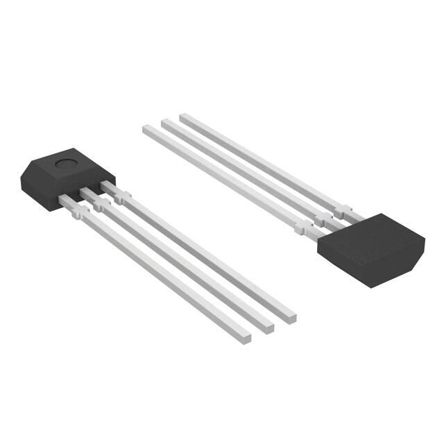
PACKAGES:
3-pin SIP,
matrix HD style
(suffix UA)
2-pin SIP
(suffix UB)
Magnetic field changes affect the two integrated Hall
transducers and then are differentially amplified on the chip.
Differential design provides immunity to radial vibration,
within the device operating air gap range, by rejection of this
common-mode signal change. Steady-state system offsets are
eliminated using an on-chip differential bandpass filter with
integrated capacitor. This filter also provides relative immunity
to interference from electromagnetic sources. The device uses
advanced temperature compensation for the high-pass filter,
sensitivity, and Schmitt trigger switchpoints to guarantee
optimal operation to low frequencies over a wide range of air
gaps and temperatures.
Continued on next page...
Not to scale
VS+
VCC
(Pin 1)
Regulator
10 nF
(UA Package Only)
Bandpass Filter Integrated
Tracking Capacitor
Dual Hall
Transducers
Comparator
Hall
Amp
Gain
Stage
VREF
Output
Control
UA Package: GND (Pin 2 or Pin 3)
UB Package: GND (Pin 2)
Figure 1: Functional Block Diagram
A17201-DS, Rev. 4
MCO-0000390
January 7, 2020
�Two-Wire AC-Coupled Differential Sensor IC
with Integrated Filter Capacitor
A17201
DESCRIPTION (continued)
The device includes: a voltage regulator, two Hall transducers,
temperature compensating circuitry, a signal conditioning amplifier,
bandpass filter, Schmitt trigger, and an output control. The on-board
regulator permits operation with supply voltages from 3.5 to 24 V.
wheel speed applications. The device packages have an operating
ambient temperature range of –40°C to 150°C, and are provided in a
3-pin plastic SIP (suffix UA) or a 2-pin plastic SIP (suffix UB). Both
packages are lead (Pb) free, with 100% matte-tin-plated leadframes.
The regulated current output is configured for two-wire interface
circuitry and is ideally suited for obtaining speed information in
SELECTION GUIDE
[1]
Packing [1]
Operating Ambient
Temperature Range,
TA (°C)
ICC(LOW) min
ICC(LOW) max
3-pin through hole SIP
Bulk, 500 pieces per bag
–40 to 150
3
7
2-pin through hole SIP
4000 pieces per 13-inch reel
–40 to 150
3
7
Part Number
Package
A17201LUAA
A17201LUBBTN
Supply Current
Contact Allegro for additional packing options.
ABSOLUTE MAXIMUM RATINGS
Characteristic
Symbol
Notes
Rating
Unit
Supply Voltage
VCC
28
V
Reverse Supply Voltage
VRCC
–18
V
Operating Ambient Temperature
TA
–40 to 150
°C
Maximum Junction Temperature
TJ(MAX)
165
°C
Tstg
–65 to 170
°C
Storage Temperature
Range L
Allegro MicroSystems
955 Perimeter Road
Manchester, NH 03103-3353 U.S.A.
www.allegromicro.com
2
�Two-Wire AC-Coupled Differential Sensor IC
with Integrated Filter Capacitor
A17201
PINOUT DIAGRAMS AND TERMINAL LIST
Terminal List
Name
1
1
2
2
Number
UA Package
UB Package
Description
VCC
1
1
Supply Voltage
GND
2
2
Ground
GND
3
–
Ground
3
UA Package
Pinout Diagram
UB Package
Pinout Diagram
INTERNAL DISCRETE CAPACITOR RATINGS (UB PACKAGE ONLY)
Characteristic
Nominal Capacitance
Symbol
CSUPPLY
Test Conditions
Connected between VCC and GND
Value (Typ.)
Unit
10
nF
Allegro MicroSystems
955 Perimeter Road
Manchester, NH 03103-3353 U.S.A.
www.allegromicro.com
3
�Two-Wire AC-Coupled Differential Sensor IC
with Integrated Filter Capacitor
A17201
OPERATING CHARACTERISTICS: Valid throughout full operating and temperature ranges, unless otherwise noted
Characteristics
Symbol
Test Conditions
Min.
Typ. [1]
Max.
Unit
3.5
12
24
V
ELECTRICAL CHARACTERISTICS
Supply Voltage [2]
Reverse Supply
Current [3]
VCC
Operating, TJ < TJ(MAX)
IRCC
VCC = –18 V
–
–
–1
mA
Supply Zener Current
IZSUPPLY
VCC = 28 V
–
–
19
mA
Supply Zener Clamp Voltage
VZSUPPLY
ICC = ICC(MAX) + 3 mA, TA = 25°C
28
33
37
V
ICC(LOW)
Low-current state
3
–
7
mA
ICC(HIGH)
High-current state
12.0
–
16.0
mA
–
7
15
ms
Supply Current
RESPONSE CHARACTERISTICS
Power-On Time [4][5]
Settling
Time [5][6]
Response Time [5]
tPO
VCC > VCC(MIN)
tSETTLING
fBdiff ≥ 100 Hz
tRESPONSE Equal to tPO + tSETTLING; fBdiff ≥ 100 Hz
–
–
310
ms
–
–
325
ms
Upper Corner Frequency [7]
fCU
–3 dB, single pole
20
–
–
kHz
Lower Corner Frequency [7]
fCL
–3 dB, single pole
–
–
8
Hz
No load (UA package only)
7
–
–
mA/μs
OUTPUT CHARACTERISTICS
[8]
Output Slew Rate Time
dI/dt
Output Rise Time
tr
ΔI/Δt from 10% to 90% ICC level; corresponds to
measured output slew rate with CSUPPLY
–
–
5.5
μs
Output Fall Time
tf
ΔI/Δt from 90% to 10% ICC; corresponds to
measured output slew rate with CSUPPLY
–
–
5.5
μs
MAGNETIC CHARACTERISTICS
Operate Point [9]
BOP
Bdiff increasing, fBdiff = 200 Hz,
Bdiff = 50 Gp-p,
ICC switches from low to high
–
7
17.4
G
Release Point [8]
BRP
Bdiff decreasing, fBdiff = 200 Hz,
Bdiff = 50 Gp-p,
ICC switches from high to low
–17.4
–7
–
G
BHYS
fBdiff = 200 Hz, Bdiff = 50 Gp-p
–
14
–
G
Bdiff
Differential p-p magnetic field
–
–
1250
G
Hysteresis [8]
Applied Magnetic
Field [10]
Typical values are at TA = 25°C and VCC = 12 V. Performance may vary for individual units, within the specified maximum and minimum limits.
Maximum voltage must be adjusted for power dissipation and junction temperature; see Power Derating section.
[3] Negative current is defined as conventional current coming out of (sourced from) the specified device terminal.
[4] Time required to initialize device.
[5] See Definitions of Terms section.
[6] Time required for the output switchpoints to be within specification.
[7] The specification is based on statistical evaluation of a limited sample population.
[8] Load circuit is R = 100 Ω and C = 10 pF. Pulse duration measured at threshold of ((I
L
L
CC(HIGH) + ICC(LOW)) / 2).
[9] For lower frequencies, the absolute values of B , B , and B
OP
RP
HYS may decrease due to delay induced by the high-pass filter.
[10] Exceeding the maximum magnetic field may result in compromised absolute accuracy.
[1]
[2]
Allegro MicroSystems
955 Perimeter Road
Manchester, NH 03103-3353 U.S.A.
www.allegromicro.com
4
�Two-Wire AC-Coupled Differential Sensor IC
with Integrated Filter Capacitor
A17201
THERMAL CHARACTERISTICS: May require derating at maximum conditions; see application information
Characteristic
Symbol
Test Conditions
RθJA
Package Thermal Resistance
Value
Units
Package UA, 1-layer PCB with copper limited to solder pads
165
°C/W
Package UB, 1-layer PCB with copper limited to solder pads
213
°C/W
Power Derating Curve
26
VCC(max)
Maximum Allowable VCC (V)
24
22
20
UA Package RθJA = 165°C/W
18
16
14
UB Package RθJA = 213°C/W
12
10
8
6
VCC(min)
4
2
0
20
40
60
80
100
120
140
160
180
Ambient Temperature, TA (ºC)
Power Dissipation versus Ambient Temperature
1000
Power Dissipation, PD (mW)
900
800
700
600
UA Package RθJA = 165°C/W
500
400
300
200
UB Package RθJA = 213°C/W
100
0
20
40
60
80
100
120
140
160
180
Ambient Temperature, TA (ºC)
Allegro MicroSystems
955 Perimeter Road
Manchester, NH 03103-3353 U.S.A.
www.allegromicro.com
5
�A17201
Two-Wire AC-Coupled Differential Sensor IC
with Integrated Filter Capacitor
DEFINITION OF TERMS
The following provides additional information about some of the
parameters cited. For additional information, visit the Allegro
website at www.allegromicro.com.
Power-On Time, tPO – The time needed by the device, after
power is applied, to initialize all circuitry necessary for proper
operation.
Applied Magnetic Field, Bdiff – The differential magnetic flux
density, which is calculated as the arithmetic difference of the
flux densities observed by each of the two Hall elements. fBdiff is
the input signal frequency.
Settling Time, tSETTLING – The time required by the device,
after tPO, and after a valid magnetic signal has been applied, to
provide proper output transitions. Settling time is a function of
magnetic offset, offset polarity, signal phase, signal frequency,
and signal amplitude.
Output Off Switchpoint (Operate Point), BOP – The value
of increasing differential magnetic flux density at which the output signal, ICC switches from ICC(LOW) to ICC(HIGH).
Output On Switchpoint (Release Point), BRP – The value
of decreasing differential magnetic flux density at which the
output signal, ICC from ICC(HIGH) to ICC(LOW).
Response Time, tRESPONSE – The total time required for
generating zero-crossing output transitions after initialization (the
sum of Power-On Time and Settling Time).
Allegro MicroSystems
955 Perimeter Road
Manchester, NH 03103-3353 U.S.A.
www.allegromicro.com
6
�Two-Wire AC-Coupled Differential Sensor IC
with Integrated Filter Capacitor
A17201
APPLICATIONS INFORMATION
The A17201 is a versatile high-precision differential sensor IC
that can be used in a wide range of applications. Proper choice
of the target material and shape, magnet material and shape, and
assembly techniques enables large working air gaps and high
switchpoint accuracy over the device operating temperature
range.
Device Operation
The A17201 contains two integrated Hall transducers that are
used to differentially respond to a magnetic field across the
surface of the IC. As shown in Figure 2, the trigger switches
the output signal ICC high when the differential magnetic field
crosses the BOP level while increasing in strength (referred to as
the positive direction) and switches the output signal, ICC low
when the differential magnetic field crosses BRP while decreasing
(the negative direction).
Start-Up
During power-on time, tPO, the output signal, ICC is high. Beyond
this time, if the applied magnetic field, Bdiff, is smaller than
BHYS, the switching state and output polarity are indeterminate.
ICC will be valid for Bdiff > BHYS, after the additional settling
time, tSETTLING, has also elapsed.
Delay
The bandpass filter induces delay in the output signal, ICC, relative to the applied magnetic field, Bdiff. Simulation data shown
in the Characteristic Data section quantify the effect of the input
signal amplitude on the phase shift of the output. Positive values
of delay indicate a lagging output, while negative values indicate
a leading output.
Applied Magnetic BOP
Field, Bdiff BRP
Output Signal, ICC
ICC(HIGH)
ICC(LOW)
Figure 2: Typical Output Characteristic
Allegro MicroSystems
955 Perimeter Road
Manchester, NH 03103-3353 U.S.A.
www.allegromicro.com
7
�Two-Wire AC-Coupled Differential Sensor IC
with Integrated Filter Capacitor
A17201
AC-Coupled Operation
Power Supply Protection
Steady-state magnet and system offsets are eliminated using an
on-chip differential bandpass filter. The upper and lower cutoff
frequencies of this patented filter are set using an internal integrated capacitor. The differential structure of this filter improves
the ability of the IC to reject single-ended noise on the GND
or VCC lines and, as a result, makes the device more resistant
to EMI (electromagnetic interference) typically seen in hostile
remote-sensing environments.
The device contains an on-chip voltage regulator and can operate
over a wide supply voltage range. In applications that operate
the device from an unregulated power supply, transient protection must be added externally. For applications using a regulated
line, EMI/RFI protection may still be required. The circuit shown
in Figure 3 is the most basic configuration required for proper
device operation.
Typical Circuit
A resistor sense, RL, to exhibit two wire output between GND
and Pin 2, is shown in Figure 3.
VCC
VCC
1
1
VCC
VCC
A17201UA
10 nF
CBYPASS
A17201UB
GND
GND
2/3
RL
100 Ω
2
CL
RL
100 Ω
CL
Figure 3: Typical Application Circuits
Allegro MicroSystems
955 Perimeter Road
Manchester, NH 03103-3353 U.S.A.
www.allegromicro.com
8
�Two-Wire AC-Coupled Differential Sensor IC
with Integrated Filter Capacitor
A17201
POWER DERATING
The device must be operated below the maximum junction
temperature of the device, TJ(max). Under certain combinations of
peak conditions, reliable operation may require derating supplied
power or improving the heat dissipation properties of the application. This section presents a procedure for correlating factors
affecting operating TJ. (Thermal data is also available on the
Allegro MicroSystems Web site.)
The Package Thermal Resistance, RθJA, is a figure of merit summarizing the ability of the application and the device to dissipate
heat from the junction (die), through all paths to the ambient air.
Its primary component is the Effective Thermal Conductivity, K,
of the printed circuit board, including adjacent devices and traces.
Radiation from the die through the device case, RθJC, is relatively
small component of RθJA. Ambient air temperature, TA, and air
motion are significant external factors, damped by overmolding.
The effect of varying power levels (Power Dissipation, PD), can
be estimated. The following formulas represent the fundamental
relationships used to estimate TJ, at PD.
PD = VIN × IIN
ΔT = PD × RθJA
(1)
(2)
TJ = TA + ΔT (3)
For example, given common conditions such as: TA= 25°C,
VCC = 3.5 V, ICC = 12 mA, and RθJA = 165°C/W, then:
Example: Reliability for VCC at TA = 150°C, package UA, using
single-layer PCB.
Observe the worst-case ratings for the device, specifically:
RθJA = 165°C/W, TJ(max) = 165°C, VCC(max) = 24 V, and
ICC(max) = 16 mA (Note: ICC(LOW) = 7 mA, ICC(HIGH) = 16 mA
with a duty cycle of 50.0% and a worst case means ICC of
11.5 mA).
Calculate the maximum allowable power level, PD(max). First,
invert equation 3:
ΔTmax = TJ(max) – TA = 165°C – 150°C = 15°C
This provides the allowable increase to TJ resulting from internal
power dissipation. Then, invert equation 2:
PD(max) = ΔTmax ÷ RθJA = 15°C ÷ 165°C/W = 90 mW
Finally, invert equation 1 with respect to voltage:
VCC(est) = PD(max) ÷ ICC(max) = 90 mW ÷ 11.5 mA = 7.8 V
The result indicates that, at TA, the application and device can
dissipate adequate amounts of heat at voltages ≤VCC(est).
Compare VCC(est) to VCC(max). If VCC(est) ≤ VCC(max), then reliable operation between VCC(est) and VCC(max) requires enhanced
RθJA. If VCC(est) ≥ VCC(max), then operation between VCC(est) and
VCC(max) is reliable under these conditions.
PD = VCC × ICC = 3.5 V × 12 mA = 42 mW
ΔT = PD × RθJA = 42 mW × 165°C/W = 6.9°C
TJ = TA + ΔT = 25°C + 6.9°C = 31.9°C
A worst-case estimate, PD(max), represents the maximum allowable power level (VCC(max), ICC(max)), without exceeding TJ(max),
at a selected RθJA and TA.
Allegro MicroSystems
955 Perimeter Road
Manchester, NH 03103-3353 U.S.A.
www.allegromicro.com
9
�Two-Wire AC-Coupled Differential Sensor IC
with Integrated Filter Capacitor
A17201
PACKAGE OUTLINE DRAWING
For Reference Only – Not for Tooling Use
(Reference DWG-0000404, Rev. 1)
NOT TO SCALE
Dimensions in millimeters
Dimensions exclusive of mold flash, gate burrs, and dambar protrusions
Exact case and lead configuration at supplier discretion within limits shown
+0.08
4.09 –0.05
45°
B
C
E
E
1.40
1.30
1.52 ±0.05
1.44 E
+0.08
3.02 –0.05
E E1
10°
Mold Ejector
Pin Flash Protrusion
E2 E
Branded
Face
0.51 REF
45°
D Standard Branding Reference View
0.79 REF
1.02
MAX
XXX
A
1
2
3
1
Line 1: Logo A
Line 2: 3-digit assigned brand
+0.03
0.41 –0.06
14.99 ±0.25
+0.05
0.43 –0.07
A
Dambar removal protrusion (6×)
B
Gate and tie bar burr area
C
Active Area Depth, 0.50 ±0.08 mm
D
Branding scale and appearance at supplier discretion
E
Hall elements (E1, E2), not to scale
1.27 NOM
Figure 4: Package UA, 3-pin SIP
Allegro MicroSystems
955 Perimeter Road
Manchester, NH 03103-3353 U.S.A.
www.allegromicro.com
10
�Two-Wire AC-Coupled Differential Sensor IC
with Integrated Filter Capacitor
A17201
PACKAGE OUTLINE DRAWING
For Reference Only – Not for Tooling Use
(Reference DWG-0000408, Rev. 3)
Dimensions in millimeters
Dimensions exclusive of mold flash, gate burrs, and dambar protrusions
Exact case and lead configuration at supplier discretion within limits shown
+0.06
4.00 –0.05
B
4 × 10°
E
1.30
1.50 ±0.05
E
1.35
0.65 ±0.07
C
1.34 E
4.00
+0.06
–0.07
E E1
E2 E
Branded
Face
A
4 × 2.50 ±0.10
0.25 REF
0.30 REF
XXXXX
Date Code
Lot Number
Mold Ejector
Pin Indent
45°
1
D
0.85 ±0.05
Standard Branding Reference View
Line 1: 5-digit Part Number
Line 2: 4-digit Date Code
Line 3: Characters 5, 6, 7, 8
of Assembly Lot Number
0.42 ±0.05
2.54 REF
4 × 0.85 REF
1
18.00 ±0.10
2
1.00 ±0.05
12.20 ±0.10
+0.07
0.25 –0.03
4 × 7.37 REF
1.80
±0.10
A
Dambar removal protrusion (8×)
B
Gate and tie bar burr area
C
Active Area Depth, 0.38 mm ±0.03
D
Branding scale and appearance at supplier discretion
E
Hall elements (E1 and E2); not to scale
F
Molded Lead Bar for alignment during shipment
0.38 REF
0.25 REF
4 × 0.85 REF
0.85 ±0.05
1.80
+0.06
–0.07
F
4.00
+0.06
–0.05
1.50 ±0.05
Figure 5: Package UB, 2-pin SIP
Allegro MicroSystems
955 Perimeter Road
Manchester, NH 03103-3353 U.S.A.
www.allegromicro.com
11
�Two-Wire AC-Coupled Differential Sensor IC
with Integrated Filter Capacitor
A17201
Revision History
Number
Date
Description
–
March 12, 2018
1
September 4, 2018
Initial release
Changed part number
2
November 30, 2018
Updated part numbers in selection guide
3
April 12, 2019
4
January 7, 2020
Updated selection guide (page 2) and supply current (page 4)
Updated capacitor values (pages 1, 38), part numbers (page 2), and Output Rise and Fall Time
values (page 4)
Copyright 2020, Allegro MicroSystems.
Allegro MicroSystems reserves the right to make, from time to time, such departures from the detail specifications as may be required to permit
improvements in the performance, reliability, or manufacturability of its products. Before placing an order, the user is cautioned to verify that the
information being relied upon is current.
Allegro’s products are not to be used in any devices or systems, including but not limited to life support devices or systems, in which a failure of
Allegro’s product can reasonably be expected to cause bodily harm.
The information included herein is believed to be accurate and reliable. However, Allegro MicroSystems assumes no responsibility for its use; nor
for any infringement of patents or other rights of third parties which may result from its use.
Copies of this document are considered uncontrolled documents.
For the latest version of this document, visit our website:
www.allegromicro.com
Allegro MicroSystems
955 Perimeter Road
Manchester, NH 03103-3353 U.S.A.
www.allegromicro.com
12
�