1. 物料型号:
- 型号:SI-3000ZD系列
2. 器件简介:
- 描述:表面贴装式低压差线性稳压器集成电路。
- 特点:紧凑的表面贴装封装(TO263-5)、最大输出电流3.0A、低压差电压:VoIF ≤ 0.6V(在Io = 3.0A时)、输出关闭时的低电路电流:Iq(OFF) ≤ 1uA、内置过热保护电路。
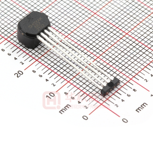
3. 引脚分配:
- VC:控制电压(输出开启时为高电平,输出关闭时为低电平)。
- w:地线(GND)。
- e:输入电压(VIN)。
- t:输出电压(VO)。
- Sense(ADJ,仅SI-3011ZD):用于输出电压调整。
4. 参数特性:
- 输入电压:VIN' = 10V
- 输出控制端电压:Ve = 6V
- 输出电流:Io'1 = 3.0A
- 功率耗散:P3 = 3W
- 结温:T = -30至+125℃
- 工作环境温度:Top = -30至+85℃
- 存储温度:Tdg = -40至+125℃
- 热阻(结到环境空气):6 = 33.3°C/W
- 热阻(结到外壳):心 = 3°C/W
5. 功能详解:
- 输出电压调整:通过连接R1和R2来设置输出电压,推荐R2值为10kΩ或11kΩ。
- 过流保护:启动电流Is1 = 3.2A。
6. 应用信息:
- 应用:二次稳定电源供电(如汽车电源)。
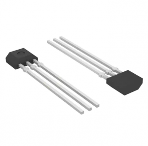
7. 封装信息:
- 封装类型:塑料模具封装,阻燃等级:UL94V-0。
- 产品重量:约1.48g。
- 外部尺寸:TO263-5封装。