1-1-1 Linear Regulator ICs
SI-3000ZFE Series 5-Terminal, Low Dropout Voltage Linear Regulator ICs
■Features
• Compact full-mold package (equivalent to TO220) • Output current: 3.0A • Low dropout voltage: VDIF ≤ 0.7V (at IO = 3.0A) • Low circuit current at output OFF: Iq (OFF) ≤ 1µA • Built-in overcurrent and thermal protection circuits
■Absolute Maximum Ratings
Parameter DC Input Voltage Output Control Terminal Voltage DC Output Current Power Dissipation Junction Temperature Operating Ambient Temperature Storage Temperature Thermal Resistance (Junction to Case) Thermal Resistance (Junction to Ambient Air) Symbol VIN*1 VC IO*1 PD1 PD2 Tj Top Tstg Ratings 10 6 3.0 20 (With infinite heatsink) 1.5 (Without heatsink, stand-alone operation) –30 to +125 –30 to +100 –30 to +125 5.0 66.7 (Without heatsink, stand-alone operation) V V A W W °C °C °C
(Ta = 25°C) Unit
■Applications
• Secondary stabilized power supply (local power supply)
θ j-c θ j-a
°C/W °C/W
■Recommended Operating Conditions
Parameter Input Voltage Output Current Operating Ambient Temperature Operating Junction Temperature Output Voltage Variable Range Symbol VIN IO Top (a) Top (j) VOADJ Ratings
*2
Unit V A °C °C V
to 6*1
0 to 3 –20 to +85 –20 to +100 1.2 to 5
*1: VIN (max) and IO (max) are restricted by the relationship PD = (VIN - VO) × IO. *2: Set the input voltage to 2.4V or higher when setting the output voltage to 2.0V or lower.
■Electrical Characteristics
Parameter Symbol min. Reference Voltage Line Regulation Load Regulation Dropout Voltage Quiescent Circuit Current Circuit Current at Output OFF Temperature Coefficient of Output Voltage Ripple Rejection Overcurrent Protection Starting Current*2
*4
(Ta = 25°C, VC = 2V unless otherwise specified)
SI-3011ZFE typ. 1.100 VIN=VO+1V, IO=10mA 10 VIN=3.3 to 5V, IO=10mA (VO=2.5V) 40 VIN=3.3V, IO=0 to 3A (VO=2.5V) 0.7 IO=3A (VO=2.5V) 1 VIN=VO+1V, IO=0A, VC=2V 1 VIN=VO+1V, VC=0V ± 0.3 Tj=0 to 100°C 60 VIN=VO+1V, f=100 to 120HZ, IO=0.1A 3.2 VIN=VO+1V 2 0.8 100 VC=2.7V –5 0 VC=0V 1.5 max. 1.122 V mV mV V mA 1.078 Unit
VADJ Conditions ∆VOLINE Conditions ∆VOLOAD Conditions VDIF Conditions Iq Conditions Iq (OFF) Conditions ∆VO/∆Ta Conditions RREJ Conditions IS1 Conditions VC, IH VC, IL IC, IH Conditions IC, IL Conditions
µA
mV/ °C dB A V
Control Voltage (Output ON)*3 Control Voltage (Output OFF)*3 VC Control Current(Output ON) Terminal Control Current(Output OFF)
µA µA
*1: *2: *3: *4:
Set the input voltage to 2.4V or higher when setting the output voltage to 2.0V or lower. IS1 is specified at the 5% drop point of output voltage VO under the Output Voltage parameter conditions. Output is OFF when the output control terminal VC is open. Each input level is equivalent to LS-TTL level. Therefore, the device can be driven directly by LS-TTLs. These products cannot be used in the following applications because the built-in foldback-type overcurrent protection may cause errors during start-up stage. (1) Constant current load (2) Positive and negative power supply (3) Series-connected power supply (4) VO adjustment by raising ground voltage
38
ICs
�SI-3000ZFE Series
■External Dimensions (TO220F-5)
Type A
±0.1
(unit : mm) Type B
10.16
±0.2
4.7
3.3
±0.2
0.5
2.54 0.7
±0.2
±0.2
φ 3.2±0.2
10.0
±0.2
4.2 ±0.2 2.8
4.0±0.2 7.9±0.2
±0.2
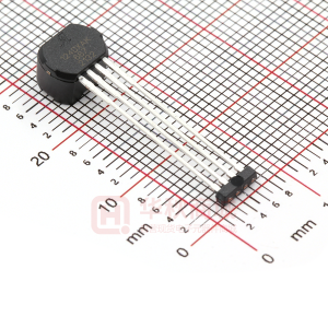
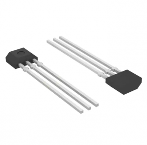
a. Part Number b. Lot number c. Administer number Pin Assignment q VC w VIN e GND r Vo t ADJ Plastic Mold Package Type Flammability: UL94V-0 Product Mass: Approx. 2.3g The external dimension shall be either A or B.
5.4
±0.2
6.68
A SK C B
.2
(17.9)
2.76
±0.2
A
B
2.6±0.1
(2.0)
(2)
0.8
±0.6
0.95
+0.1 R-end
±0.15 +0.2
4 × p1.7 9.6
±0.2
±0.6
0.5 –0.1
+0.2
4.3 8.2
±0.7
±0.7
4.3
0.85 –0.1 P1.7±0.7×4=6.8±0.7
0.45 –0.1
+0.2
3.9±0.7
(4.3) 8.2±0.7
1234
5
12345
■Typical Connection Diagram/Block Diagram
SI-3011ZFE
VIN
+
2
4
VO
R3
*
CIN REF
+ +
R1
+
Drive TSD OCP AMP1
5 ADJ CO R2
CIN: Input capacitor (Approx. 10µF) This capacitor is required when the input line contains inductance or when the wiring is long. CO: Output capacitor (47µF or higher) The output voltage may oscillate if a low ESR type capacitor (such as a ceramic capacitor) is used for the output capacitor in SI-3000ZFE. R1, R2: Output voltage setting resistors The output voltage can be set by connecting R1 and R2 as shown at left. The recommended value for R2 is 10kΩ or 11kΩ.
VC
ON/ OFF 1
+
3 GND
R1= (VO–VADJ) / (VADJ/R2)
*: Insert R3 in case of setting VO to VO ≤ 1.8V. The recommended value for R3 is 10kΩ.
■Ta-PD Characteristics
25 With Silicone Grease Heatsink: Aluminum
Power Dissipation PD (W)
20
With Infinite Heatsink
15
200×200×2mm (2.3°C/W) 100×100×2mm (5.2°C/W) 75×75×2mm (7.6°C/W)
10
5 Without heatsink 0 –30 0 25 50 75 100
Ambient Temperature Ta (°C)
4.6±0.6
0.5 –0.05
(4.6)
5.0±0.6
(17.9)
3.
2
±0
C
16.9±0.3
15.87
-
φ
ICs
39
�
很抱歉,暂时无法提供与“SI-3011ZFE”相匹配的价格&库存,您可以联系我们找货
免费人工找货