Re L i n gu e a lat r ors
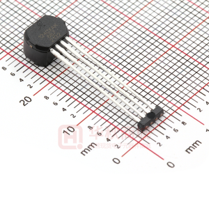
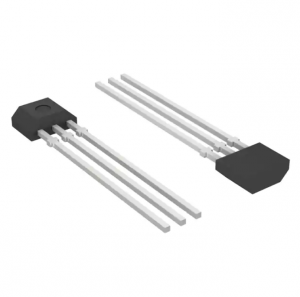
SI-3018LSA
LOW-VOLTAGE, HIGH-CURRENT 1.8 V LINEAR REGULATOR
IN INTERNAL CONNECTION SUPPLY ENABLE
1 2 3 4 8
OUT OUT GND GND
The SI-3018LSA is designed to meet the requirement for increased integration and reliability in low-voltage, high-current, linear regulator applications such as personal computers (PCs) and set-top boxes. Each device incorporates a monolithic low-level reference and control circuit with a high-current pnp transistor in a power multi-chip module (PMCM™). Regulated output voltages of 2.5 V or 3.3 V are also available. The high-current pass element provides an output current to 1 A. Regulator accuracy of ±2 % and excellent temperature characteristics are provided. The logic-compatible ENABLE input gives the designer complete control over power up, power down, and standby or sleep. These devices are supplied in a fully molded 8-lead miniature surface-mount package (tape and reel) with enhanced power-dissipating qualities. They are rated for continuous operation between -30°C and
Data Sheet 27468.18*
IC VR VS SUB
7 6 5
Dwg. PK-012
ABSOLUTE MAXIMUM RATINGS
Input Voltage, VI ................................ 16 V Supply Voltage, VS ............................ 16 V Continuous Output Current, IO ........ 1.0 A* Logic Input Voltage, VE ......................... VS Package Power Dissipation, PD ........................................ See Graph Output Junction Temperature, TJ ............................................ +150°C† Operating Temperature Range, TA ............................... -30°C to +100°C Storage Temperature Range, Tstg ............................. -30°C to +150°C
* Output current rating may be limited by duty cycle, ambient temperature, and heat sinking. Under any set of conditions, do not exceed the specified current rating or a junction temperature of 150˚C. † Fault conditions that produce excessive junction temperature will activate the device’s thermal protection circuitry. These conditions can be tolerated but should be avoided.
+100°C.
FEATURES
s s s s s 1 A Output Current LSTTL/CMOS-Compatible On/Off Control Less Than 1 µA “Sleep” Current Internal Foldback Overcurrent Limiting Internal Thermal Protection Surface-Mount Package
Always order by complete part number: SI-3018LSA-TL , where “-TL” indicates tape and reel.
Sanken Power Devices from Allegro MicroSystems
™
�FUNCTIONAL BLOCK DIAGRAM
INPUT 1 INTERNAL CONNECTION 2 8 OUTPUT
SUPPLY
3
THERMAL PROTECTION
SUB +
ENABLE
4
GROUND
5
Leads 7 and 8 are soldered to the copper area and provide heat sinking of the pass transistor.
RECOMMENDED OPERATING CONDITIONS
Max. Input Voltage, VI ................................................ 3.5 V Output Current, IO .......................................... 0 A to 1.0 A Output Junction Temperature Range, TJ -20 °C to +125°C Ambient Temperature Range, TA .............. -30°C to +85°C For the availability of parts meeting -40°C requirements, contact Allegro’s Sales Representative.
This data sheet is based on Sanken data sheet SSJ-01835.
2
115 Northeast Cutoff, Box 15036 Worcester, Massachusetts 01615-0036 (508) 853-5000 Copyright © 2001, 2005 Allegro MicroSystems, Inc.
Re L i n gu e a lat r ors
7 OUTPUT 6 GROUND
Dwg. FK-019
TM
SI-3018LSA LOW-VOLTAGE, HIGH-CURRENT 1.8 V LINEAR REGULATOR
�ELECTRICAL CHARACTERISTICS at TA = +25°C, VI = VS = 3.3 V, VE = 2.0 V (unless otherwise noted).
Limits Characteristic Output Voltage Symbol VO VOQ Output Volt. Temp. Coeff. Overcurrent Limit Line Regulation Load Regulation Dropout Voltage Ground Terminal Current aVO IOM ∆VO(∆VI) ∆VO(∆IO) VImin - VO IGND IQ Rejection Ratio ENABLE Input Voltage PSRR VEH VEL ENABLE Input Current IEH IEL Thermal Protection Temp. Thermal Resistance TJ RθJL To terminals 7 and 8 Test Conditions IO = 500 mA VE = 0 V, Output Off IO = 5 mA, 0°C ≤ TJ ≤ 100°C VO = 95% of VO at IO = 500 mA 3.1 V ≤ VI = VS ≤ 3.5 V, IO = 300 mA 0 ≤ IO ≤ 1 A IO ≤ 1 A IO = 0 mA VE = 0 V, IO = 0 mA 100 Hz ≤ f ≤ 120 Hz Output On Output Off VE = 2 V, Output On VE = 0 V, Output Off Min. 1.764 — — 1.2 — — — — — — 2.0 — — — 135 — Typ. 1.800 — ±0.3 1.5 2.0 10 0.55 1.7 — 60 — — 30 0 150 36 Max. 1.836 0.5 — — 10 20 1.2 2.5 1.0 — — 0.8 80 -5.0 — — Units V V mV/°C A mV mV V mA µA dB V V µA µA °C °C/W
Re L i n gu e a lat r ors
SI-3018LSA LOW-VOLTAGE, HIGH-CURRENT 1.8 V LINEAR REGULATOR
Typical values are at TA = +25°C and are given for circuit design information only.
www.allegromicro.com
3
�TYPICAL CHARACTERISTICS at TA = 25°C
Dropout voltage
0.6
1.86
Load regulation
0.5
1.84
DROPOUT VOLTAGE
OUTPUT VOLTAGE
0.4
1.82
0.3
1.80
0.2
1.78
0.1
1.76
0 0 0.2 0.4 0.6 0.8 1.0 1.2
Dwg. GK-025
1.74 0 0.2 0.4 0.6 0.8 1.0 1.2
Dwg. GK-026
OUTPUT CURRENT in AMPERES
OUTPUT CURRENT in AMPERES
Overcurrent protection
2.0
2.0
VOUT vs VIN
VI = VS = 3.2 V 1.5 VI = VS = 5 V VI = VS = 6 V
1.5 IO = 0 A
OUTPUT VOLTAGE
OUTPUT VOLTAGE
IO = 0.5 A 1.0 IO = 1 A
1.0
0.5
0.5
0 0 0.5 1.0 1.5 2.0
Dwg. GK-027
0 0 1.0 2.0 3.0 4.0 5.0
Dwg. GK-028
OUTPUT CURRENT in AMPERES
INPUT VOLTAGE
4
115 Northeast Cutoff, Box 15036 Worcester, Massachusetts 01615-0036 (508) 853-5000
Re L i n gu e a lat r ors
VI = VS = 8 V VI = VS = 5 V VI = VS = 3.2 V
TM
SI-3018LSA LOW-VOLTAGE, HIGH-CURRENT 1.8 V LINEAR REGULATOR
�Re L i n gu e a lat r ors
SI-3018LSA LOW-VOLTAGE, HIGH-CURRENT 1.8 V LINEAR REGULATOR
TYPICAL CHARACTERISTICS at TA = 25°C (cont’d)
Line regulation GND current
20
1.86
1.84
15
GROUND CURRENT in mA
OUTPUT VOLTAGE
1.82
IO = 1 A IO = 0.5 A 10 IO = 0 A
1.80 IO = 1 A 1.78 IO = 0.5 A IO = 0 A 1.76
5.0
1.74 0 2.0 4.0 6.0 8.0 10 12
Dwg. GK-029
0 0 2.0 4.0 6.0 8.0 10 12
Dwg. GK-030
INPUT VOLTAGE
INPUT VOLTAGE
ENABLE input current
60
50
VI = VS = 3.3 V IO = 5 mA
ENABLE INPUT CURRENT in µ A
40
30
20
10
0 0 0.5 1.0 1.5 2.0 2.5 3.0
Dwg. GK-023
ENABLE VOLTAGE in VOLTS
www.allegromicro.com
5
�APPLICATIONS INFORMATION
Thermal protection and heat sinking. Thermal protection circuitry turns off the device should the junction temperature rise above 135°C. This is intended only to protect the device from failures due to excessive junction temperatures and should not imply that high-temperature operation is permitted. Ambient temperature is affected by air circulation and proximity to other heat-producing components. Normal operation is resumed when the junction temperature is reduced. Output terminals 7 and 8 are the lead frame and substrate of the pass transistor and provide a low thermal-resistance path for heat sinking. In general, the maximum ambient temperature has the most effect on determining the heat sinking that is needed to maintain a safe normal operating junction temperature. The maximum heat sinking thermal resistance (RθJA) can be calculated as RθJA = (135 – TA) / IO (VI – 1.8) where TA is the maximum ambient temperature in °C, IO is the maximum output (load) current in amperes, and VI is the maximum input voltage in volts. The following graph gives the required copper foil area (soldered to leads 7 and 8) to provide the required thermal resistance. Note that more is always better and both sides of the printed wiring board can be used. ENABLE input. The ENABLE input includes an internal pull2000 GLASS-EPOXY PRINTED WIRING BOARD 1000
down resistor. If this terminal is not connected (open-circuit fault), the device output is turned off. Overcurrent protection. The SI-3018LSA includes an overcurrent protection circuit, which limits the output current at start up. It thus cannot be used with 1) a constant-current load, 2) a power supply with positive and negative to a common load (center-tap type power supply), 3) a series power supply, or 4) a diode or resistor in series with the device ground to raise the output voltage. Input voltage. Including ripple voltage and transients, the minimum input voltage should be greater than the sum of the output voltage and the maximum rated dropout voltage; the maximum input voltage must be less than the absolute maximum rated input voltage (16 V). In most applications, the input voltage (terminal 1, VI) and the supply voltage (terminal 3, VS) are connected together. Output capacitor. A 22 µF tantalum electrolytic capacitor is recommended between the output and ground. Very-low ESR capacitors should not be used. Input capacitor. A 0.1 µF to 10 µF tantalum capacitor is recommended between the input and ground to prevent oscillation.
FOIL AREA in SQ. mm
500
300
200
100 90 100 110 120 130
Dwg. GK-031
JUNCTION-TO-AMBIENT THERMAL RESISTANCE in ° C/W
6
115 Northeast Cutoff, Box 15036 Worcester, Massachusetts 01615-0036 (508) 853-5000
Re L i n gu e a lat r ors
TM
SI-3018LSA LOW-VOLTAGE, HIGH-CURRENT 1.8 V LINEAR REGULATOR
�Re L i n gu e a lat r ors
SI-3018LSA LOW-VOLTAGE, HIGH-CURRENT 1.8 V LINEAR REGULATOR
Dimensions in Millimeters
(controlling dimensions)
8
7
6
5
0.25 0.10
±0.2
4.4
±0.3 ±0.1
6.2
0.5
±0.1
0.4
1
±0.4
1.27
BSC
0° TO 10°
5.1
1.55
±0.15
0.10 MAX.
Dwg. MK-006-8 mm
NOTES: 1. Exact body and lead configuration at vendor’s option within limits shown. 2. Lead spacing tolerance is non-cumulative. 3. Leads 7 and 8 are internally connected together and provide heat sinking of the pass transistor.
www.allegromicro.com
7
�Tape and Reel Dimensions in Millimeters
(controlling dimensions)
1.55
CENTER LINES OF CAVITY 0.7
4.0
0.3 2.5
2.0
5.5
8.0
COVER TAPE
USER DIRECTION OF UNREELING
2.0
Dwg. MA-015-1
ACCESS HOLE 2.0 15.4 ± 1.0 (MEASURED AT HUB
180
13 ± 0.2
60
13.0 ± 0.3 (MEASURED AT HUB TAPE SLOT IN CORE FOR TAPE START
Dwg. MA-018-1
115 Northeast Cutoff, Box 15036 Worcester, Massachusetts 01615-0036 (508) 853-5000
TM
8
10.25
12.0
5.6
Re L i n gu e a lat r ors
SI-3018LSA LOW-VOLTAGE, HIGH-CURRENT 1.8 V LINEAR REGULATOR
�The products described herein are manufactured in Japan by Sanken Electric Co., Ltd. for sale by Allegro MicroSystems, Inc. Sanken and Allegro reserve the right to make, from time to time, such departures from the detail specifications as may be required to permit improvements in the performance, reliability, or manufacturability of its products. Therefore, the user is cautioned to verify that the information in this publication is current before placing any order. When using the products described herein, the applicability and suitability of such products for the intended purpose shall be reviewed at the users responsibility. Although Sanken undertakes to enhance the quality and reliability of its products, the occurrence of failure and defect of semiconductor products at a certain rate is inevitable. Users of Sanken products are requested to take, at their own risk, preventative measures including safety design of the equipment or systems against any possible injury, death, fires or damages to society due to device failure or malfunction. Sanken products listed in this publication are designed and intended for use as components in general-purpose electronic equipment or apparatus (home appliances, office equipment, telecommunication equipment, measuring equipment, etc.). Their use in any application requiring radiation hardness assurance (e.g., aerospace equipment) is not supported. When considering the use of Sanken products in applications where higher reliability is required (transportation equipment and its control systems or equipment, fire- or burglar-alarm systems, various safety devices, etc.), contact a Sanken sales representative to discuss and obtain written confirmation of your specifications. The use of Sanken products without the written consent of Sanken in applications where extremely high reliability is required (aerospace equipment, nuclear powercontrol stations, life-support systems, etc.) is strictly prohibited. The information included herein is believed to be accurate and reliable. Application and operation examples described in this publication are given for reference only and Sanken and Allegro assume no responsibility for any infringement of industrial property rights, intellectual property rights, or any other rights of Sanken or Allegro or any third party that may result from its use.
Re L i n gu e a lat r ors
SI-3018LSA LOW-VOLTAGE, HIGH-CURRENT 1.8 V LINEAR REGULATOR
www.allegromicro.com
9
�