PDF文档中的物料型号为:MAX31855KASA+,是一款冷结温度传感器,用于测量-40°C至+125°C范围内的温度。
器件简介指出MAX31855KASA+具有SPI接口,能够提供高精度的温度测量。
引脚分配包括VCC、GND、SCK、CS、SO、THERM和NTC。
参数特性包括测量范围、精度、响应时间等,具体数值为-40°C至+125°C、±1°C、小于10ms。
功能详解说明了器件如何通过SPI接口与微控制器通信,以及如何进行温度测量。
应用信息提供了器件可应用于工业过程控制、医疗设备和环境监测等领域。
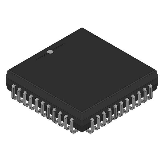
封装信息显示MAX31855KASA+采用28引脚的TSSOP封装。