8-Line EMI Filter with Integrated ESD Protection
AOZ8040
General Description
The AOZ8040 is an 8-line device integrating EMI filtering with ESD protection for each line. It is designed to suppress unwanted EMI/RFI signals and provide electrostatic discharge (ESD) protection in portable electronic equipment. This state-of-the-art device utilizes AOS leading edge Trench Vertical Structure [TVS]2 ™ technology for superior clamping performance and filter attenuation over the full operating display range. The AOZ8040 has been optimized for protection of color LCD displays and CCD camera lines in cellular phones and other portable consumer electronic devices. The AOZ8040 consists of eight identical circuits comprised of TVS diodes for ESD protection, and a resistor–capacitor network for EMI/RFI filtering. A series resistor value of 100Ω and a capacitance value of 9pF are used to achieve -20dB minimum attenuation from 1.0GHz to 3.0GHz. The TVS diodes provide effective suppression of ESD voltages in excess of ±20kV (air discharge) and ±20kV (contact discharge). This exceeds IEC 61000-4-2, level 4 ESD immunity test. The AOZ8040 comes in an RoHS compliant, 1.2mm x 3.5mm, 0.4mm pitch DFN package and is rated over a -40°C to +85°C ambient temperature range.
Features
●
8 lines for EMI filtering and ESD protection: – Exceeds IEC 61000-4-2, level 4 (ESD) immunity test – ±20kV (air discharge) and ±20kV (contact discharge) Trench Vertical Structure [TVS]2 ™ based technology used to achieve excellent ESD clamping & filter performance over the full operating display range Filter performance: -20db attenuation from 1.0GHz to 3.0GHz Low operating voltage: 5.0V Capacitance stability over wide range of voltages and temperatures DFN package: 1.2mm x 3.5mm, 0.4mm pitch Pb-Free device Green product
●
● ● ● ● ● ●
Applications
● ● ●
EMI filtering and ESD protection for data lines LCD displays, camera interface, I/O interface Portable handheld devices, cell phones, PDA phones
Typical Application
D0
100Ω
CH1
9pF 9pF
100Ω
D1
CH2
LCD/Camera Module
9pF
9pF
D7
100Ω
CH8
9pF 9pF
Figure 1.
Rev. 1.2 March 2010
www.aosmd.com
Page 1 of 7
�AOZ8040
Ordering Information
Part Number
AOZ8040DI
Ambient Temperature Range
-40°C to +85°C
Package
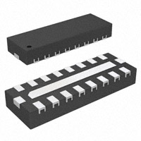
DFN-16
Environmental
RoHS Compliant Green Product
AOS Green Products use reduced levels of Halogens, and are also RoHS compliant. Please visit www.aosmd.com/web/quality/rohs_compliant.jsp for additional information.
Pin Configuration
1 16
16 15
1 2
2
15
3
14
Exposed Pad (GND)
14 13 12 11 10 9
3
4 13
4 5 6
6 11 5 12
7 8
7 10
DFN-16
(Bottom View)
8
9
Top View
Pin Description
Pin Number
1,16 2, 15 3, 14 4, 13 5, 12 6, 11 7, 10 8, 9 Exposed Pad
Pin Name
CH 1 CH 2 CH 3 CH 4 CH 5 CH 6 CH 7 CH 8 GND
Pin Function
Channel 1 Connections Channel 2 Connections Channel 3 Connections Channel 4 Connections Channel 5 Connections Channel 6 Connections Channel 7 Connections Channel 8 Connections Common Ground Connection
Rev. 1.2 March 2010
www.aosmd.com
Page 2 of 7
�AOZ8040
Absolute Maximum Ratings
Exceeding the Absolute Maximum ratings may damage the device.
Parameter
Storage Temperature (TS) ESD Rating per IEC61000-4-2, contact ESD Rating per IEC61000-4-2, air
(1) (1)
Rating
-65°C to +150°C ±20kV ±20kV ±30kV
ESD Rating per Human Body Model(2)
Notes: 1. IEC 61000-4-2 discharge with CDischarge = 150pF, RDischarge = 330Ω.
2. Human Body Discharge per MIL-STD-883, Method 3015 CDischarge = 100pF, RDischarge = 1.5kΩ.
Electrical Characteristics
TA = 25°C unless otherwise specified.
Symbol
VRWM VBR IR VCL
Parameter
Reverse Working Voltage Reverse Breakdown Voltage Reverse Leakage Current Signal Clamp Voltage
(3)
Conditions
IT = 1mA(4)
Min.
6
Typ.
7
Max.
5.0 8 0.1
Units
V V µA V
VRWM = 3.3V ILOAD = 1A, positive ILOAD = 1A, negative clamp(5)(8) ILOAD = 5A, positive clamp(5)(8) ILOAD = 5A, negative clamp(5)(8) ILOAD = 12A, positive clamp(5)(8) ILOAD = 12A, negative clamp(5)(8) clamp(5)(8)
7.0 -3.0 8.0 -5.0 10.0 -10.0 90 8 100 9 250 -20 110 10
RCH CCH fC
Total Series Resistance Channel Capacitance Cut-off Frequency Attenuation from 1.0GHz to 3.0GHz
IR = 20mA Input to Ground(6)(7)(8) Measured with 50Ω source and 50Ω load termination VR = 0V Measured with 50Ω source and 50Ω load termination
Ω
pF MHz dB
Notes: 3. The working peak reverse voltage, VRWM, should be equal to or greater than the DC or continuous peak operating voltage level. 4. VBR is measured at the pulse test current IT. 5. Measurements performed using a 100ns Transmission Line Pulse (TLP) system. 6. Total capacitance is equal to 2 x CCH. 7. Measured at 25°C, VR = 2.5V, f = 1.0MHz. 8. Guaranteed by design.
Rev. 1.2 March 2010
www.aosmd.com
Page 3 of 7
�AOZ8040
Typical Performance Characteristics
Insertion Loss Characteristics
0 -5 -10 Insertion Loss (dB) -15 S21 (db) -20 -25 -30 -35 -40 -45 -50 -120 -120 1 10 100 Frequency (MHz) 1000 10000 1 10 100 Frequency (MHz) 1000 10000 -20 -40 -60 -80 0
Crosstalk Crosstalk (I/O-I/O) vs. Frequency
-100
Clamping Voltage vs. Peak Pulse Current
11
Forward Voltage vs. Forward Current
12
(tperiod = 100ns, tr = 1ns)
(tperiod = 100ns, tr = 1ns)
Clamping Voltage, Vcl (V)
10 Forward Voltage (V)
10
9
8
8
6
7
4
6 0 2 4 6 8 10 12 Peak Pulse Current, Ipp (A)
2 0 2 4 6 8 10 12 Forward Current (A)
Typical Resistance vs. Temperature
110
105 Resistance (Ω)
100
95
90 -45
-25
-5
5
25
45
65
85
Temparature (°C)
Rev. 1.2 March 2010
www.aosmd.com
Page 4 of 7
�AOZ8040
Package Dimensions, DFN 3.5 x 1.2, 16L
D b D1
E L Pin 1 Marking
E1
TOP VIEW
e
BOTTOM VIEW
Pin 1 ID (C0.2x45°)
A
A1
SIDE VIEW
A3
RECOMMENDED LAND PATTERN
2.80 0.15 0.20 0.20 0.15 0.20
Dimensions in millimeters
Symbols A A1 A3 b D D1 Min. 0.50 0.00 Nom. 0.55 Max. 0.60
Dimensions in inches
Symbols A A1 A3 b D D1 E E1 e L Min. 0.020 0.000 Nom. 0.022 Max. 0.024
— 0.05 0.152 Ref. 0.15 0.20 0.25 3.45 2.75 1.15 0.25 0.20 3.50 2.80 3.55 2.85
— 0.002 0.006 Ref. 0.006 0.008 0.010 0.136 0.108 0.045 0.010 0.008 0.138 0.110 0.140 0.112
0.30
1.00
E E1 e L
1.20 1.25 0.30 0.35 0.40 BSC 0.25 0.30
0.047 0.049 0.012 0.014 0.016 BSC 0.010 0.012
0.30 0.40 0.20
Notes: 1. All dimensions are in millimeters. Angles is degree. 2. Warpage shall not exceed 0.10mm. 3. Marking is for package orientation reference only.
Rev. 1.2 March 2010
www.aosmd.com
Page 5 of 7
�AOZ8040
Tape & Reel Dimensions, DFN 3.5 x 1.2, 16L
Carrier Tape
K0 P1 P2 D0 E1 E2 B1 B0 E (B2) (A2) A0 A1 UNIT: mm Package DFN 3.5x1.2 T 0.30 ±0.05 B0 3.80 ±0.1 B1 3.75 ±0.1 B2 4.16 A0 1.50 ±0.1 A1 1.45 ±0.1 A2 1.86 K0 0.75 ±0.1 D0 ø1.55 ±0.05 E 12.00 ±0.3 E1 1.75 ±0.1 E2 5.50 ±0.05 0.15 P0
0.15 T
Feeding Direction P0 4.00 ±0.10 P1 4.0 ±0.1 P2 2.00 ±0.05
Reel
B W1
S K 60° 120° M N
H
2.84 B 2.24 W
Arbor Hole Detail A Scale 2:1 Front View
Back View
Unit: mm Tape Size Reel Size 12mm ø1800
Section: B-B
M ø179.0 +1.0
N ø60.0 ±0.5
W 13.0 ±0.5
W1 17.0
H ø13.0 ±0.2
K 10.5 ±0.25
S 1.8 (Bottom)
Leader / Trailer & Orientation
Trailer Tape 300mm Min.
Components Tape Orientation in Pocket
Leader Tape 500mm Min.
Rev. 1.2 March 2010
www.aosmd.com
Page 6 of 7
�AOZ8040
Package Marking
H1F
Part Number Code Assembly Lot Code Week and Year Code
Alpha & Omega Semiconductor reserves the right to make changes to this data sheet at any time without notice. LIFE SUPPORT POLICY ALPHA & OMEGA SEMICONDUCTOR PRODUCTS ARE NOT AUTHORIZED FOR USE AS CRITICAL COMPONENTS IN LIFE SUPPORT DEVICES OR SYSTEMS. As used herein: 1. Life support devices or systems are devices or systems which, (a) are intended for surgical implant into the body or (b) support or sustain life, and (c) whose failure to perform when properly used in accordance with instructions for use provided in the labeling, can be reasonably expected to result in a significant injury of the user. 2. A critical component in any component of a life support, device, or system whose failure to perform can be reasonably expected to cause the failure of the life support device or system, or to affect its safety or effectiveness.
Rev. 1.2 March 2010
www.aosmd.com
Page 7 of 7
�