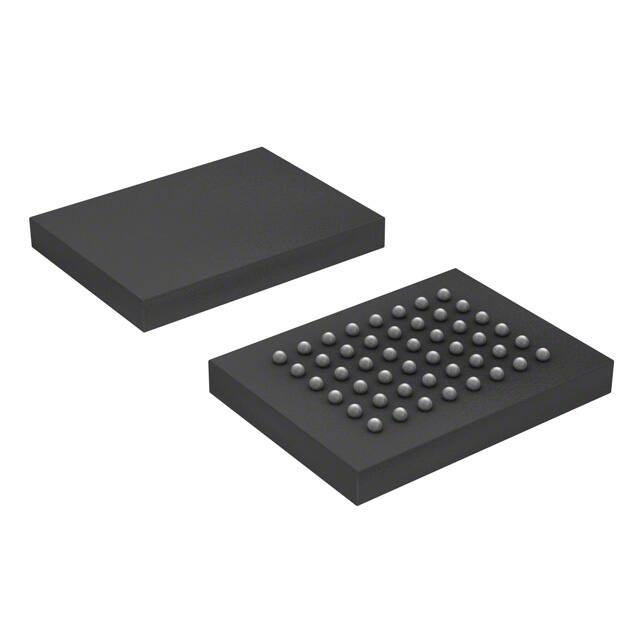
AS1C1M16P-70BIN
Revision History
16M (1M x 16 bit) PSEUDO STATIC RAM
48ball FPBGA Package
Revision
Rev 1.0
Details
Preliminary datasheet
Date
Aug 2018
Alliance Memory Inc. 511 Taylor Way, San Carlos, CA 94070 TEL: (650) 610-6800 FAX: (650) 620-9211
Alliance Memory Inc. reserves the right to change products or specification without notice
Confidential
- 1 of 11 -
Rev.1.0 Aug. 2018
�AS1C1M16P-70BIN
1Mb x16 Pseudo Static RAM Specification
GENERAL DESCRIPTION
The AS1C1M16P-70BIN is 16,777,216 bits of Pseudo SRAM which uses DRAM type memory cells, but
this device has refresh-free operation and extreme low power consumption technology. Furthermore the
interface is compatible to a low power Asynchronous type SRAM. The AS1C1M16P-70BIN is
organized as 1,048,576 Words x 16 bit.
FEATURES
- Organization :1M x16
- Address access speed 70ns
- Power Supply Voltage : 2.6 ~ 3.3V
- Separated I/O power(VccQ) & Core power(Vcc)
- Three state outputs
- Byte read/write control by UB# / LB#
- Auto-TCSR for power saving
- - Package type : 48ball-FPBGA (6.0x7.0)
- - Operating Temperature
- . Industrial : -40 ℃ ~ 85 ℃
PRODUCT FAMILY
Power Dissipation
Operating
Temp.
Part Number
Power
Supply
Operating ICC ( Max.)
Speed
(tRC)
Standby
(ISB, Max.)
AS1C1M16P-70BIN
-40oC to 85oC
2.6 ~ 3.3V
70ns
120uA
ICC1
( f = 1MHz)
5mA
ICC2
( f = fmax)
25mA
FUNCTION BLOCK DIAGRAM
ZZ#
CS#
UB#
LB#
WE#
OE#
CONTROL
LOGIC
A0~A19
ADDRESS
DECODER
DQ0~
DQ15
Self-Refresh
CONTROL
ROW SELECT
COLUMN SELECT
Memory Array
1M X 16
Din/Dout BUFFER
I/O CIRCUIT
Confidential
- 2 of 11 -
Rev.1.0 Aug. 2018
�AS1C1M16P-70BIN
PIN DESCRIPTION(48-FPBGA-6.00 x 7.00)
2
1
3
4
5
6
A
LB#
OE#
A0
A1
A2
ZZ#
B
DQ8
UB#
A3
A4
CS#
DQ0
C
DQ9
DQ10
A5
A6
DQ1
DQ2
D
VSSQ
DQ11
A17
A7
DQ3
VCC
E
VCCQ
DQ12
DNU
A16
DQ4
VSS
F
DQ14
DQ13
A14
A15
DQ5
DQ6
G
DQ15
A19
A12
A13
WE#
DQ7
H
A18
A8
A9
A10
A11
NC
TOP VIEW (Ball Down)
Name
Function
Name
Function
CS#
Chip select input
LB#
Lower byte (DQ0~7)
OE#
Output enable input
UB#
Upper byte (DQ8~15)
WE#
Write enable input
VCC
Power supply
ZZ#
Connected with VCC in this version VCCQ
I/O power supply
DQ0-15
Data in-out
VSS(Q)
Ground
A0-19
Address inputs
NC
No connection
DNU
Do not use
Confidential
- 3 of 11 -
Rev.1.0 Aug. 2018
�AS1C1M16P-70BIN
ABSOLUTE MAXIMUM RATINGS 1)
Parameter
Symbol
Ratings
Voltage on Any Pin Relative to Vss
VIN, VOUT
Voltage on Vcc supply relative to Vss
VCC, VCCQ
-0.2 to VCCQ+0.3V
V
-0.22) to VCCQ+0.3V
V
PD
1.0
TSTG
-65 to 150
o
TA
-40 to 85
o
Power Dissipation
Storage Temperature
Unit
Operating Temperature
W
C
C
1. Stresses greater than those listed above “Absolute Maximum Ratings” may cause permanent damage to the device.
Functional operation should be restricted to recommended operating condition. Exposure to absolute maximum rating conditions for
extended periods may affect reliability.
2. Undershoot at power-off : -1.0V in case of pulse width < 20ns
FUNCTIONAL DESCRIPTION
CS#
OE#
WE#
LB#
UB#
DQ0~7
DQ8~15
Mode
Power
H
X
X
X
X
High-Z
High-Z
Deselected
Stand by
L
H
H
L
X
High-Z
High-Z
Output Disabled
Active
L
H
H
X
L
High-Z
High-Z
Output Disabled
Active
L
L
H
L
H
Data Out
High-Z
Lower Byte Read
Active
L
L
H
H
L
High-Z
Data Out
Upper Byte Read
Active
L
L
H
L
L
Data Out
Data Out
Word Read
Active
L
X
L
L
H
Data In
High-Z
Lower Byte Write
Active
L
X
L
H
L
High-Z
Data In
Upper Byte Write
Active
L
X
L
L
L
Data In
Data In
Word Write
Active
Note:
1. X means don’t care. (Must be low or high state)
Confidential
- 4 of 11 -
Rev.1.0 Aug. 2018
�AS1C1M16P-70BIN
RECOMMENDED DC OPERATING CONDITIONS 1)
Parameter
Symbol
Min
Typ
Max
Unit
VCC
2.6
3.0
3.3
V
VCCQ
2.6
3.0
3.3
V
VSS, VSSQ
0
0
0
V
Input high voltage
VIH
0.8 * VCCQ
-
VCCQ + 0.22)
V
Input low voltage
VIL
-
0.2 * VCCQ
V
Supply voltage
Ground
1.
2.
3.
4.
-0.23)
TA= -30 to 85oC, otherwise specified
Overshoot: VCC +1.0 V in case of pulse width < 20ns
Undershoot: -1.0 V in case of pulse width < 20ns
Overshoot and undershoot are sampled, not 100% tested.
CAPACITANCE1) (f =1MHz, TA=25oC)
Item
Symbol
Test Condition
Min
Max
Unit
Input capacitance
CIN
VIN=0V
-
8
pF
Input/Output capacitance
CIO
VIO=0V
-
8
pF
1. Capacitance is sampled, not 100% tested
DC AND OPERATING CHARACTERISTICS
Parameter
Symbol
Test Conditions
Min
Typ
Max
Unit
Input leakage current
ILI
VIN=VSS to VCCQ , VCC=VCCmax
-1
-
1
uA
Output leakage current
ILO
CS#=VIH , OE#=VIH or WE#=VIL ,
VIO=VSS to VCCQ , VCC=VCCmax
-1
-
1
uA
-
-
5
mA
Average operating current
ICC1
Cycle time = 1us, IIO=0mA, 100% duty,
CS#VCCQ-0.2V, Other inputs = 0 ~ VCCQ
Standby current (CMOS)
ISB
(Typ. condition : VCC=3.0V @ 25oC)
(Max. condition : VCC=3.3V @ 85oC)
1. Maximum Icc specifications are tested with VCC = VCCmax.
Confidential
- 5 of 11 -
Rev.1.0 Aug. 2018
�AS1C1M16P-70BIN
AC OPERATING CONDITIONS
Dout
Test Conditions (Test Load and Test Input/Output Reference)
Input Pulse Level : 0.2V to VCCQ-0.2V
Input Rise and Fall Time : 5ns
Input and Output reference Voltage : VCCQ/2
CL1)
Output Load (See right) : CL1) = 30pF
1. Including scope and Jig capacitance
AC CHARACTERISTICS
Read
Write
Speed
Symbol
Parameter List
Unit
Min
Max
Read Cycle Time
tRC
70
10k
ns
Address access time
tAA
-
70
ns
Chip enable to data output
tCO
-
70
ns
Output enable to valid output
tOE
-
25
ns
UB#, LB# enable to data output
tBA
-
25
ns
Chip enable to low-Z output
tLZ
10
-
ns
UB#, LB# enable to low-Z output
tBLZ
0
-
ns
Output enable to low-Z output
tOLZ
0
-
ns
Chip disable to high-Z output
tHZ
0
20
ns
UB#, LB# disable to high-Z output
tBHZ
0
20
ns
Output disable to high-Z output
tOHZ
0
20
ns
Output hold from Address change
tOH
5
-
ns
Write Cycle Time
tWC
70
10k
ns
Chip enable to end of write
tCW
60
-
ns
Address setup time
tAS
0
-
ns
Address valid to end of write
tAW
60
-
ns
UB#, LB# valid to end of write
tBW
60
-
ns
Write pulse width
tWP
50
-
ns
Write recovery time
tWR
0
-
ns
Write to output high-Z
tWHZ
0
20
ns
Data to write time overlap
tDW
20
-
ns
Data hold from write time
tDH
0
-
ns
End write to output low-Z
tOW
5
-
ns
Confidential
- 6 of 11 -
Rev.1.0 Aug. 2018
�AS1C1M16P-70BIN
TIMING DIAGRAMS
READ CYCLE (1) (Address controlled, CS#=OE#=VIL, WE#=VIH, UB# or/and LB#=VIL)
tRC
Address
tAA
tOH
Data Out
Data Valid
Previous Data Valid
READ CYCLE (2) (WE#=VIH)
tRC
Address
tAA
CS#
tOH
tCO
tHZ
tBA
LB#, UB#
tBHZ
tOE
OE#
Data Out
High-Z
tOLZ
tBLZ
tOHZ
Data Vaild
tLZ
NOTES (READ CYCLE)
1. tHZ , tBHZ and tOHZ are defined as the time at which the outputs achieve the open circuit conditions and are not referenced
to output voltage levels.
2. Do not Access device with cycle timing shorter than tRC for continuous periods > 10us.
Confidential
- 7 of 11 -
Rev.1.0 Aug. 2018
�AS1C1M16P-70BIN
WRITE CYCLE (1) (WE# controlled)
tWC
Address
tAW
tCW
CS#
tBW
LB#,UB#
WE#
tAS
Data In
tWR
tWP
tDH
tDW
High-Z
Data Valid
tWHZ
tOW
Data Undefined
Data Out
WRITE CYCLE (2) (CS# controlled)
tWC
Address
tAS
CS#
tWR
tCW
tAW
LB#,UB#
tBW
WE#
tWP
tDH
tDW
Data In
Data Out
Data Valid
High-Z
WRITE CYCLE (3) (UB#/LB# controlled)
tWC
Address
tWR
tCW
CS#
tAW
tAS
LB#,UB#
tBW
tWP
WE#
tDW
Data Valid
Data In
Data Out
Confidential
tDH
High-Z
- 8 of 11 -
Rev.1.0 Aug. 2018
�AS1C1M16P-70BIN
NOTES (WRITE CYCLE)
1. A write occurs during the overlap(tWP) of low CS#, low WE# and low UB# or LB#. A write begins at the last
transition among low CS# and low WE# with asserting UB# or LB# low for single byte operation or simultaneously
asserting UB# and LB# low for word operation. A write ends at the earliest transition among high CS# and high WE#.
The tWP is measured from the beginning of write to the end of write.
2. tCW is measured from CS# going low to end of write.
3. tAS is measured from the address valid to the beginning of write.
4. tWR is measured from the end of write to the address change. tWR applied in case a write ends as CS# or WE# going high.
5. Do not access device with cycle timing shorter than tWC for continuous periods > 10us.
TIMING WAVEFORM OF POWER UP
200us
VCC(Min.)
VCC
CS#
Power Up Mode
Normal Operation
NOTE ( POWER UP )
1. After Vcc reaches Vcc(Min.) , wait 200us with CS# high. Then you get into the normal operation.
Confidential
- 9 of 11 -
Rev.1.0 Aug. 2018
�AS1C1M16P-70BIN
Unit: millimeters
PACKAGE DIMENSION
48 Ball Fine Pitch BGA (0.75mm ball pitch)
Confidential
- 10 of 11 -
Rev.1.0 Aug. 2018
�AS1C1M16P-70BIN
PART NUMBERING SYSTEM
AS1C
PSEUDO
SRAM
1M16P
1M16=1Mx16
P=PSEUDO
SRAM
-70
B
I
N
70ns
B = FPBGA
I=Industrial
(-40° C~+85° C)
Indicates Pb
and Halogen
Free
XX
Packing Type
None:Tray
TR:Reel
Alliance Memory, Inc.
511 Taylor Way,
San Carlos, CA 94070
Tel: 650-610-6800
Fax: 650-620-9211
www.alliancememory.com
Copyright © Alliance Memory
All Rights Reserved
© Copyright 2007 Alliance Memory, Inc. All rights reserved. Our three-point logo, our name and Intelliwatt are
trademarks or registered trademarks of Alliance. All other brand and product names may be the trademarks of their
respective companies. Alliance reserves the right to make changes to this document and its products at any time
without notice. Alliance assumes no responsibility for any errors that may appear in this document. The data
contained herein represents Alliance's best data and/or estimates at the time of issuance. Alliance reserves the right
to change or correct this data at any time, without notice. If the product described herein is under development,
significant changes to these specifications are possible. The information in this product data sheet is intended to be
general descriptive information for potential customers and users, and is not intended to operate as, or provide, any
guarantee or warrantee to any user or customer. Alliance does not assume any responsibility or liability arising out of
the application or use of any product described herein, and disclaims any express or implied warranties related to the
sale and/or use of Alliance products including liability or warranties related to fitness for a particular purpose,
merchantability, or infringement of any intellectual property rights, except as express agreed to in Alliance's Terms
and Conditions of Sale (which are available from Alliance). All sales of Alliance products are made exclusively
according to Alliance's Terms and Conditions of Sale. The purchase of products from Alliance does not convey a
license under any patent rights, copyrights; mask works rights, trademarks, or any other intellectual property rights of
Alliance or third parties. Alliance does not authorize its products for use as critical components in life-supporting
systems where a malfunction or failure may reasonably be expected to result in significant injury to the user, and the
inclusion of Alliance products in such life-supporting systems implies that the manufacturer assumes all risk of such
use and agrees to indemnify Alliance against all claims arising from such use.
Confidential
- 11 of 11 -
Rev.1.0 Aug. 2018
�


 工商网监
湘ICP备2023018690号
工商网监
湘ICP备2023018690号