2Gb/4Gb/8Gb LPDDR4
Revision History
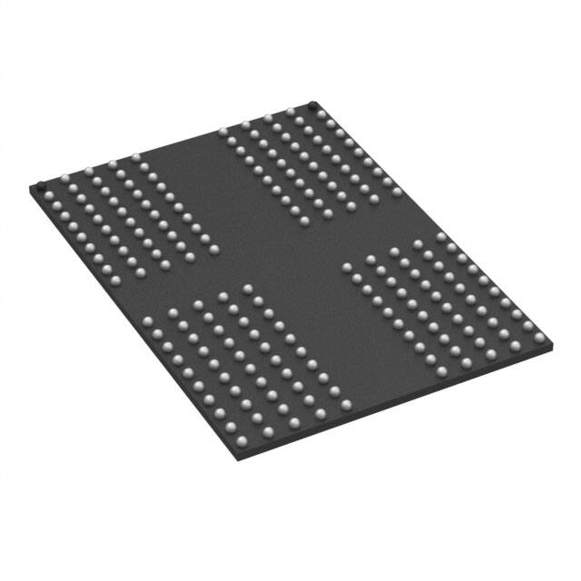
For 2Gb/4Gb/8Gb LPDDR4 200ball FBGA Package
Revision
Details
Date
Rev 1.0
Initial Release
Aug 2020
Confidential
- 1 of 64 -
Rev. 1.0 Aug. 2020
�2Gb/4Gb/8Gb LPDDR4
1 Overview
The LPDDR4 SDRAM is organized as 1 or 2 channels per device, and individual channel is 8-banks and 16-bits.
This product uses a double-data-rate architecture to achieve high-speed operation. The double data rate architecture is
essentially a 16n prefetch architecture with an interface designed to transfer two data words per clock cycle at the I/O pins.
This product offers fully synchronous operations referenced to both rising and falling edges of the clock. The data paths
are internally pipelined and 16n bits prefetched to achieve very high bandwidth.
1.1 Features
The 2Gb/4Gb/8Gb LPDDR4 SDRAM offers the
following key features:
Configuration:
- x32 for 2-channels per device (AS4C64M32MD4 ,
AS4C128M32MD4, AS4C256M32MD4)
- x16 for 1-channel per device
(AS4C128M16MD4, AS4C256M16MD4)
- 8 internal banks per each channel
On-Chip ECC:
- Single-bit error correction (per 64-bits), which will
maximize reliability
- Optional ERR output signal per channel, which
indicates ECC event occurrence
- ECC Register, which controls ECC function
Low-voltage Core and I/O Power Supplies:
- VDD2 /VDDQ = 1.06-1.17V, VDD1 = 1.70-1.95V
LVSTL(Low Voltage Swing Terminated Logic) I/O
Interface
Internal VREF and VREF Training
Dynamic ODT :
- DQ ODT :VSSQ Termination
- CA ODT :VSS Termination
Selectable output drive strength (DS)
Max. Clock Frequency : 1.6GHz (3.2Gbps for one
channel)
16-bit Pre-fetch DDR data bus
Single data rate (multiple cycles) command/address
bus
Bidirectional/differential data strobe per byte of data
(DQS, DQS)
DMI pin support for write data masking and DBI
functionality
Programmable READ and WRITE latencies (RL/WL)
Programmable and on-the-fly burst lengths (BL =16,
32)
Support non-targert DRAM ODT control
Directed per-bank refresh for concurrent bank
operation and ease of command scheduling
ZQ Calibration
Operation Temperature:
- Automotive A2 (TC = -40°C to 105°C)
On-chip temperature sensor to control self refresh rate
On-chip temperature sensor whose status can be
read from MR4
RoHS-compliant, “green” packaging
Package:
2Gb/4Gb : 200 ball FBGA (10mm x 14.5mm x 0.8mm)
8Gb : 200 ball FBGA (10mm x 14.5mm x 1.1mm)
Table 1. Speed Grade Information
Speed Grade
DDR4L-3200
Clock Frequency
RL
tCK (ns)
1600MHz
28
0.625
*Other clock frequencies/data rates supported; please refer to AC timing tables
Confidential
- 2 of 64 -
Rev. 1.0 Aug. 2020
�2Gb/4Gb/8Gb LPDDR4
1.2 Product List
Table 2 shows all possible products within the 2Gbit/4Gbit/8Gbit LPDDR4 SDRAM component generation. Availability
depends on application needs.
Table2. Ordering Information for 2Gb/4Gb/8Gb LPDDR4
Product part No
Org
Temperature
Max Clock (MHz)
Package
AS4C128M16MD4-062BAN 128M x 16
Automotive -40°C to 105°C
1600
200-ball FBGA
AS4C128M32MD4-062BAN 128M x 32
Automotive -40°C to 105°C
1600
200-ball FBGA
AS4C256M16MD4-062BAN 256M x 16
Automotive -40°C to 105°C
1600
200-ball FBGA
AS4C256M32MD4-062BAN 256M x 32
Automotive -40°C to 105°C
1600
200-ball FBGA
AS4C64M32MD4-062BAN
Automotive -40°C to 105°C
1600
200-ball FBGA
Confidential
64M x 32
- 3 of 64 -
Rev. 1.0 Aug. 2020
�2Gb/4Gb/8Gb LPDDR4
1.3 Addressing
Table 4 - 2Gb/4Gb/8Gb LPDDR4 SDRAM Addressing
Memory Density
4Gb
4Gb
8Gb
2Gb
2Gb
Organization
x32
x16
x32
x32
x16
Number of Channels
2
1
2
2
1
Density per channel
2Gb
4Gb
4Gb
1Gb
2Gb
Configuration
16Mb x 16DQ x
8 banks x 2
channels
32Mb x 16DQ x
8 banks x 1
channel
32Mb x 16DQ x
8 banks x 2
channels
8Mb x 16DQ x 8
banks x 2
channels
16Mb x 16DQ x
8 banks x 1
channel
Number of Banks (per Channel)
8
8
8
8
8
Array Pre-Fetch (Bits, per channel)
256
256
256
256
266
8,192
16,384
Number of Rows (per channel)
16,384
32,768
32,768
Number of Columns (fetch boundaries)
64
64
64
64
64
Page Size (Bytes)
2,048
2,048
2048
2048
2048
BA0-BA2
BA0-BA2
BA0-BA2
BA0-BA2
BA0-BA2
R0-R13
R0-R14
R0-R14
R0-R12
R0-R13
C0-C9
C0-C9
C0-C9
C0-C9
C0-C9
64-bit
64-bit
64-bit
64-bit
64-bit
Bank Address
X16
Row
Addresses
Column
Addresses
Burst Starting Address Boundary
NOTE 1 The lower two column addresses (C0 - C1) are assumed to be “zero” and are not transmitted on the CA bus.
NOTE 2 Row and Column address values on the CA bus that are not used for a particular density be at valid logic levels.
NOTE 3 For non - binary memory densities,only half of the row address space is valid. When the MSB address bit is
“HIGH”, then the MSB - 1 address bit must be “LOW”.
NOTE 4 The row address input which violates restriction described in note 3 may result in undefined or vendor specific
behavior. Consult memory vendor for more information.
Confidential
- 4 of 64 -
Rev. 1.0 Aug. 2020
�2Gb/4Gb/8Gb LPDDR4
1.4 Package Block Diagram
Figure 1 – Dual Channel Package Block Diagram
Part number: AS4C64M32MD4 ,AS4C128M32MD4, AS4C256M32MD4
Figure 2 – Single Channel Package Block Diagram
Part number: AS4C128M16MD4, AS4C256M16MD4
Confidential
- 5 of 64 -
Rev. 1.0 Aug. 2020
�2Gb/4Gb/8Gb LPDDR4
1.5 Package Ballout
Figure 3 - 200-ball x32 Discrete Package, 0.80mm x 0.65mm using MO-311
1
2
3
4
5
A
NC
NC
VSS
VDD2
B
NC
DQ0_A
VDDQ
C
VSS
DQ1 _A
D
VDDQ
E
0.80mm Pitch
6
7
8
9
10
11
12
ZQ0
NC
VDD2
VSS
ERR_A
NC
DQ7_A
VDDQ
VDDQ
DQ15_A
VDDQ
DQ8_A
NC
DMI0_A
DQ6_A
VSS
VSS
DQ14_A
DMI1 _A
DQ9_A
VSS
VSS
DQS0_T
_A
VSS
VDDQ
VDDQ
VSS
DQS1_T
_A
VSS
VDDQ
VSS
DQ2 _A
DQS0_C
_A
DQ5_A
VSS
VSS
DQ13_A
DQS1_C
_A
DQ10_A
VSS
F
VDD1
DQ3_A
VDDQ
DQ4_A
VDD2
VDD2
DQ12_A
VDDQ
DQ11 _A
VDD1
G
VSS
ODT_CA
_A
VSS
VDD1
VSS
VSS
VDD1
VSS
NC
VSS
H
VDD2
CA0_A
NC
CS0_A
VDD2
VDD2
CA2 _A
CA3_A
CA4_A
VDD2
J
VSS
CA1_A
VSS
CKE0_A
NC
CK_t_A
CK_ c_A
VSS
CA5_A
VSS
K
VDD2
VSS
VDD2
VSS
NC
NC
VSS
VDD2
VSS
VDD2
N
VDD2
VSS
VDD2
VSS
NC
NC
VSS
VDD2
VSS
VDD2
P
VSS
CA1_B
VSS
CKE0_B
NC
CK_t_B
CK_c_B
VSS
CA5_B
VSS
R
VDD2
CA0_B
NC
CS0_B
VDD2
VDD2
CA2_B
CA3_B
CA4_B
VDD2
T
VSS
ODT_CA
_B
VSS
VDD1
VSS
VSS
VDD1
VSS
RESET_
n
VSS
U
VDD1
DQ3_B
VDDQ
DQ4_B
VDD2
VDD2
DQ12_B
VDDQ
DQ11_B
VDD1
V
VSS
DQ2_B
DQS0_C
_B
DQ5_B
VSS
VSS
DQ13_B
DQS1_C
_B
DQ10_B
VSS
W
VDDQ
VSS
DQS0_T
_B
VSS
VDDQ
VDDQ
VSS
DQS1_T
_B
VSS
VDDQ
Y
VSS
DQ1_B
DMI0_B
DQ6_B
VSS
VSS
DQ14_B
DMI1_B
DQ9_B
VSS
AA
NC
DQ0_B
VDDQ
DQ7_B
VDDQ
VDDQ
DQ15_B
VDDQ
DQ8_B
NC
AB
NC
NC
VSS
VDD2
VSS
VSS
VDD2
VSS
ERR_B
NC
L
M
NOTE 1 0.8mm pitch (X-axis), 0.65mm pitch (Y-axis), 22 rows.
NOTE 2 Top View, A1 in top left corner.
NOTE 3 ODT_CA_[x] balls are wired to ODT_CA_[x] pads of Rank 0 DRAM die. ODT_CA_[x] pads for other ranks (if present) are
disabled in the package.
NOTE 4 Die pad VSS and VSSQ signals are combined to VSS package balls.
NOTE 5 11A and 11AB are optional ERR signals.
Confidential
- 6 of 64 -
Rev. 1.0 Aug. 2020
�2Gb/4Gb/8Gb LPDDR4
Figure 4 - 200-ball x16 Discrete Package, 0.80mm x 0.65mm using MO-311
1
2
3
4
5
A
NC
NC
VSS
VDD2
B
NC
DQ0_A
VDDQ
C
VSS
DQ1 _A
D
VDDQ
E
0.80mm Pitch
6
7
8
9
10
11
12
ZQ0
NC
VDD2
VSS
ERR_A
NC
DQ7_A
VDDQ
VDDQ
DQ15_A
VDDQ
DQ8_A
NC
DMI0_A
DQ6_A
VSS
VSS
DQ14_A
DMI1 _A
DQ9_A
VSS
VSS
DQS0_T
_A
VSS
VDDQ
VDDQ
VSS
DQS1_T
_A
VSS
VDDQ
VSS
DQ2 _A
DQS0_C
_A
DQ5_A
VSS
VSS
DQ13_A
DQS1_C
_A
DQ10_A
VSS
F
VDD1
DQ3_A
VDDQ
DQ4_A
VDD2
VDD2
DQ12_A
VDDQ
DQ11 _A
VDD1
G
VSS
ODT_CA
_A
VSS
VDD1
VSS
VSS
VDD1
VSS
NC
VSS
H
VDD2
CA0_ A
NC
CS0_A
VDD2
VDD2
CA2 _A
CA3_A
CA4_A
VDD2
J
VSS
CA1 _ A
VSS
CKE0_A
NC
CK_t_A
CK_ c_A
VSS
CA5_A
VSS
K
VDD2
VSS
VDD2
VSS
NC
NC
VSS
VDD2
VSS
VDD2
N
VDD2
VSS
VDD2
VSS
NC
NC
VSS
VDD2
VSS
VDD2
P
VSS
NC
VSS
NC
NC
NC
NC
VSS
NC
VSS
R
VDD2
NC
NC
NC
VDD2
VDD2
NC
NC
NC
VDD2
T
VSS
NC
VSS
VDD1
VSS
VSS
VDD1
VSS
RESET_
n
VSS
U
VDD1
NC
VDDQ
NC
VDD2
VDD2
NC
VDDQ
NC
VDD1
V
VSS
NC
NC
NC
VSS
VSS
NC
NC
NC
VSS
W
VDDQ
VSS
NC
VSS
VDDQ
VDDQ
VSS
NC
VSS
VDDQ
Y
VSS
NC
NC
NC
VSS
VSS
NC
NC
NC
VSS
AA
NC
NC
VDDQ
NC
VDDQ
VDDQ
NC
VDDQ
NC
NC
AB
NC
NC
VSS
VDD2
VSS
VSS
VDD2
VSS
NC
NC
L
M
NOTE 1 0.8mm pitch (X-axis), 0.65mm pitch (Y-axis), 22 rows.
NOTE 2 Top View, A1 in top left corner.
NOTE 3 ODT_CA_[x] balls are wired to ODT_CA_[x] pads of Rank 0 DRAM die. ODT_CA_[x] pads for other ranks (if present) are
disabled in the package.
NOTE 4 Die pad VSS and VSSQ signals are combined to VSS package balls.
NOTE 5 11A is optional ERR signal.
Confidential
- 7 of 64 -
Rev. 1.0 Aug. 2020
�2Gb/4Gb/8Gb LPDDR4
1.6 Pin Functional Description
Table 5 - Pin Functional Description
Symbol
CK_t_A,
CK_c_A,
CK_t_B,
CK_c_B
CKE_A
CKE_B
CS_A
CS_B
CA[5:0]_A
CA[5:0]_B
ODT_CA_A
ODT_CA_B
DQ[15:0]_A,
DQ[15:0]_B
DQS[1:0]_t_A,
DQS[1:0]_c_A,
DQS[1:0]_t_B,
DQS[1:0]_c_B
DMI[1:0]_A,
DMI[1:0]_B
ZQ
Type
Input
Input
Input
Input
Input
I/O
Function
Clock: CK_t and CK_c are differential clock inputs. All address, command, and control input
signals are sampled on the crossing of the positive edge of CK_t and the negative edge of
CK_c. AC timings for CA parameters are referenced to CK. Each channel (A & B) has its own
clock pair.
Clock Enable: CKE HIGH activates and CKE LOW deactivates the internal clock circuits,
input buffers, and output drivers. Power-saving modes are entered and exited via CKE
transitions. CKE is part of the command code. Each channel (A & B) has its own CKE signal.
Chip Select: CS is part of the command code. Each channel (A & B) has its own CS signal.
Command/Address Inputs: CA signals provide the Command and Address inputs
according to the Command Truth Table. Each channel (A&B) has its own CA signals.
CA ODT Control: The ODT_CA pin is used in conjunction with the Mode Register to turn
on/off the On-Die-Termination for CA pins.
Data Input/Output: Bi-direction data bus.
Data Strobe: DQS_t and DQS_c are bi-directional differential output clock signals used to
strobe data during a READ or WRITE. The Data Strobe is generated by the DRAM for a
READ and is edge-aligned with Data. The Data Strobe is generated by the Memory
I/O
Controller for a WRITE and must arrive prior to Data. Each byte of data has a Data Strobe
signal pair. Each channel (A & B) has its own DQS strobes.
Data Mask Inversion: DMI is a bi-directional signal which is driven HIGH when the data on
the data bus is inverted, or driven LOW when the data is in its normal state. Data Inversion
can be disabled via a mode register setting. Each byte of data has a DMI signal. Each
I/O
channel (A & B) has its own DMI signals. This signal is also used along with the DQ signals
to provide write data masking information to the DRAM. The DMI pin function - Data
Inversion or Data mask - depends on Mode Register setting.
Calibration Reference: Used to calibrate the output drive strength and the termination
Refere
resistance. There is one ZQ pin per die. The ZQ pin shall be connected to VDDQ through a
nce
240Ω ± 1% resistor.
VDDQ,
VDD1,
VDD2
Supply Power Supplies: Isolated on the die for improved noise immunity.
VSS, VSSQ
GND
RESET_n
Input
Ground Reference: Power supply ground reference.
RESET: When asserted LOW, the RESET_n signal resets all channels of the
die. There is one RESET_n pad per die.
NOTE 1 "_A" and "_B" indicate DRAM channel "_A" pads are present in all devices. "_B" pads are present in dual channel SDRAM
devices only.
Confidential
- 8 of 64 -
Rev. 1.0 Aug. 2020
�2Gb/4Gb/8Gb LPDDR4
1.7 Power-up, Initialization and Power-off Procedure
For power-up and reset initialization, in order to prevent DRAM from functioning improperly, default values of the
following MR settings are defined as Table 6.
Table 6 - MRS defaults settings
Item
MRS
Default Setting
Description
FSP-OP/WR
MR13 OP[7:6]
00B
FSP-OP/WR[0] are enabled
WLS
MR2 OP[6]
0B
Write Latency Set 0 is selected
WL
MR2 OP[5:3]
000B
WL = 4
RL
MR2 OP[2:0]
000B
RL = 6, nRTP=8
nWR
MR1 OP[6:4]
000B
nWR = 6
DBI-WR/RD
MR3 OP[7:6]
00B
Write & Read DBI are disabled
CA ODT
MR11 OP[6:4]
000B
CA ODT is disabled
DQ ODT
MR11 OP[2:0]
000B
DQ ODT is disabled
VREF(CA) Setting
MR12 OP[6]
1B
VREF(CA) Range[1] enabled
VREF(CA) Value
MR12 OP[5:0]
001101B
Range1 : 27.2% of VDD2
VREF(DQ) Setting
MR14 OP[6]
1B
VREF(DQ) Range[1] enabled
VREF(DQ) Value
MR14 OP[5:0]
001101B
Range1 : 27.2% of VDDQ
1.7.1
Voltage Ramp and Device Initialization
The following sequence shall be used to power up the LPDDR4 device. Unless specified otherwise, these steps are
mandatory. Note that the power-up sequence of all channels must proceed simultaneously.
1. While applying power (after Ta), RESET_n is recommended to be LOW (≤0.2 x VDD2) and all other inputs must be
between VILmin and VIHmax. The device outputs remain at High-Z while RESET_n is held LOW. Power supply
voltage ramp requirements are provided in Table 7. VDD1 must ramp at the same time or earlier than VDD2. VDD2
must ramp at the same time or earlier than VDDQ.
Table 7 - Voltage Ramp Conditions
After
Ta is reached
Applicable Conditions
VDD1 must be greater than VDD2
VDD2 must be greater than VDDQ - 200 mV
NOTE 1 Ta is the point when any power supply first reaches 300 mV.
NOTE 2 Voltage ramp conditions in Table 8 apply between Ta and power-off (controlled or uncontrolled).
NOTE 3 Tb is the point at which all supply and reference voltages are within their defined ranges.
NOTE 4 Power ramp duration tINIT0 (Tb-Ta) must not exceed 20ms.
NOTE 5 The voltage difference between any of VSS and VSSQ pins must not excess 100 mV.
2. Following the completion of the voltage ramp (Tb), RESET_n must be maintained LOW. DQ, DMI, DQS_t and
DQS_c voltage levels must be between VSSQ and VDDQ during voltage ramp to avoid latch- up. CKE, CK_t, CK_c,
CS_n and CA input levels must be between VSS and VDD2 during voltage ramp to avoid latch-up.
3. Beginning at Tb, RESET_n must remain LOW for at least tINIT1(Tc), after which RESET_n can be deasserted to
HIGH(Tc). At least 10ns before RESET_n de-assertion, CKE is required to be set LOW. All other input signals are
"Don't Care".
Confidential
- 9 of 64 -
Rev. 1.0 Aug. 2020
�2Gb/4Gb/8Gb LPDDR4
1.7.1
Voltage Ramp and Device Initialization (cont’d)
NOTES : 1. Training is optional and may be done at the system architects discretion. The training sequence after ZQ_CAL Latch(Th, Sequence7~9) in Figure 5 is simplified
recommendation and actual training sequence may vary depending on systems.
Figure 5 - Power Ramp and Initialization Sequence
4. After RESET_n is de-asserted(Tc), wait at least tINIT3 before activating CKE. Clock(CK_t,CK_c) is required to be
started and stabilized for tINIT4 before CKE goes active(Td). CS is required to be maintained LOW when controller
activates CKE.
5. After setting CKE high, wait minimum of tINIT5 to issue any MRR or MRW commands(Te). For both MRR and MRW
commands, the clock frequency must be within the range defined for tCKb. Some AC parameters (for example,
tDQSCK) could have relaxed timings (such as tDQSCKb) before the system is appropriately configured.
6. After completing all MRW commands to set the Pull-up, Pull-down and Rx termination values, the DRAM controller can
issue ZQCAL Start command to the memory(Tf). This command is used to calibrate VOH level and output
impedance over process, voltage and temperature. In systems where more than one LPDDR4 DRAM devices share
one external ZQ resistor, the controller must not overlap the ZQ calibration sequence of each LPDDR4 device. ZQ
calibration sequence is completed after tZQCAL (Tg) and the ZQCAL Latch command must be issued to update the
DQ drivers and DQ+CA ODT to the calibrated values.
7. After tZQLAT is satisfied (Th) the command bus (internal VREF(CA), CS, and CA) should be trained for high-speed
operation by issuing an MRW command (Command Bus Training Mode). This command is used to calibrate the
device's internal VREF and align CS/CA with CK for high-speed operation. The LPDDR4 device will power-up with
receivers configured for low-speed operations, and VREF(CA) set to a default factory setting. Normal device
operation at clock speeds higher than tCKb may not be possible until command bus training has been completed.
NOTE The command bus training MRW command uses the CA bus as inputs for the calibration data stream, and
outputs the results asynchronously on the DQ bus. See 4.29, (item 1.), MRW for information on how to enter/exit the
training mode.
8. After command bus training, DRAM controller must perform write leveling. Write leveling mode is enabled when
MR2 OP[7] is high (Ti). See 4.31, Mode Register Write-WR Leveling Mode, for detailed description of write leveling
entry and exit sequence. In write leveling mode, the DRAM controller adjusts write DQS_t/_c timing to the point
where the LPDDR4 device recognizes the start of write DQ data burst with desired write latency.
9. After write leveling, the DQ Bus (internal VREF(DQ), DQS, and DQ) should be trained for high-speed operation
using the MPC training commands and by issuing MRW commands to adjust VREF(DQ)(Tj). The LPDDR4 device
will power-up with receivers configured for low-speed operations and VREF(DQ) set to a default factory setting.
Normal device operation at clock speeds higher than tCKb should not be attempted until DQ Bus training has been
completed. The MPC Read Calibration command is used together with MPC FIFO Write/Read commands to train
Confidential
- 10 of 64 -
Rev. 1.0 Aug. 2020
�2Gb/4Gb/8Gb LPDDR4
DQ bus without disturbing the memory array contents. See DQ Bus Training section for detailed DQ Bus Training
sequence.
10. At Tk the LPDDR4 device is ready for normal operation, and is ready to accept any valid command. Any more
registers that have not previously been set up for normal operation should be written at this time.
Table 8 - Initialization Timing Parameters
Value
Parameter
Unit
Comment
Min
Max
tINIT0
-
20
ms
Maximum voltage-ramp time
tINIT1
200
-
us
Minimum RESET_n LOW time after completion of voltage ramp
tINIT2
10
-
ns
Minimum CKE low time before RESET_n high
tINIT3
2
-
ms
Minimum CKE low time after RESET_n high
tINIT4
5
-
tCK
Minimum stable clock before first CKE high
tINIT5
2
-
us
Minimum idle time before first MRW/MRR command
tZQCAL
1
-
us
ZQ calibration time
tZQLAT
Max(30ns, 8tCK)
Note *1,2
-
ns
ZQCAL latch quiet time.
Note *1,2
ns
Clock cycle time during boot
tCKb
NOTE 1 Min tCKb guaranteed by DRAM test is 18 ns.
NOTE 2 The system may boot at a higher frequency than dictated by min tCKb. The higher boot frequency is system
dependent.
1.7.2 Reset Initialization with Stable Power
The following sequence is required for RESET at no power interruption initialization.
1. Assert RESET_n below 0.2 x VDD2 anytime when reset is needed. RESET_n needs to be maintained for minimum
tPW_RESET. CKE must be pulled LOW at least 10 ns before de-asserting RESET_n.
2. Repeat steps 4 to 10 in1.6.1.
Table 9 - Reset Timing Parameter
Value
Parameter
tPW_RESET
1.7.3
Min
Max
100
-
Unit
ns
Comment
Minimum RESET_n low Time for Reset Initialization
with stable power
Power-off Sequence
The following procedure is required to power off the device.
While powering off, CKE must be held LOW (0.2 X VDD2) and all other inputs must be between VILmin and VIHmax.
The device outputs remain at High-Z while CKE is held LOW. DQ, DMI, DQS_t and DQS_c voltage levels must be
between VSSQ and VDDQ during voltage ramp to avoid latch-up. RESET_n, CK_t, CK_c, CS and CA input levels
must be between VSS and VDD2 during voltage ramp to avoid latch-up.
Tx is the point where any power supply drops below the minimum value specified.
Tz is the point where all power supplies are below 300mV. After Tz, the device is powered off.
Table 10 - Power Supply Conditions
After
Tx and Tz
Applicable Conditions
VDD1 must be greater than VDD2
VDD2 must be greater than VDDQ - 200 mV
The voltage difference between any of VSS, VSSQ pins must not exceed 100 mV.
Confidential
- 11 of 64 -
Rev. 1.0 Aug. 2020
�2Gb/4Gb/8Gb LPDDR4
1.7.4 Uncontrolled Power-off Sequence
When an uncontrolled power-off occurs, the following conditions must be met:
At Tx, when the power supply drops below the minimum values specified, all power supplies must be turned off and all
power supply current capacity must be at zero, except any static charge remaining in the system.
After Tz (the point at which all power supplies first reach 300mV), the device must power off. During this period the
relative voltage between power supplies is uncontrolled. VDD1 and VDD2 must decrease with a slope lower than 0.5
V/μs between Tx and Tz.
An uncontrolled power-off sequence can occur a maximum of 400 times over the life of the device.
Table 11 - Timing Parameters Power Off
Confidential
Value
Symbol
Min
Max
Unit
tPOFF
-
2
s
- 12 of 64 -
Comment
Maximum Power-off ramp item
Rev. 1.0 Aug. 2020
�2Gb/4Gb/8Gb LPDDR4
1.8 Mode Register Definition
Table 12 shows the mode registers for LPDDR4 SDRAM. Each register is denoted as "R" if it can be read but not
written, "W" if it can be written but not read, and "R/W" if it can be read and written. A Mode Register Read command is
used to read a mode register. A Mode Register Write command is used to write a mode register.
Table 12 - Mode Register Assignment in LPDDR4 SDRAM
MR#
OP[7]
OP[6]
OP[5]
0
CATR
RFU
RFU
1
2
3
4
5
6
7
8
9
10
11
12
13
14
15
16
17
18
19
20
21
22
23
RPST
WR Lev
DBI-WR
TUF
24
25
26
27
28
29
30
31
32
33
34
35
36
37
38
39
40
Confidential
OP[4]
OP[3]
RZQI
OP[2]
OP[1]
RFU
RFU
nWR (for AP)
RD-PRE
WR-PRE
WLS
WL
DBI-RD
PDDS
PPRP
Thermal Offset
PPRE
SR Abort
LPDDR4 Manufacturer ID
Revision ID-1
Revision ID-2
IO Width
Density
Vendor Specific Test Register
RFU
RFU
CA ODT
RFU
RFU
VR-CA
VREF(CA)
FSP-OP
FSP-WR
DMD
RRO
VRCG
VRO
RFU
VR(dq)
VREF(DQ)
Lower-Byte Invert Register for DQ Calibration
PASR Bank Mask
PASR Segment Mask
DQS Oscillator Count - LSB
DQS Oscillator Count - MSB
Upper-Byte Invert Register for DQ Calibration
RFU
RFU
ODTD-CA
ODTE-CS
ODTE-CK
DQS interval timer run time setting
TRR Mode
TRR Mode BAn
Unlimited
MAC
OP[0]
Refresh
mode
BL
RL
WR PST
PU-CAL
Refresh Rate
Type
ZQ-Reset
DQ ODT
RPT
CBT
SOC ODT
MAC Value
PPR Resource
RFU
RFU
RFU
RFU
Reserved for testing - SDRAM will ignore
RFU
D Calibration Pattern “A” (default = 5AH)
ECC control
ECC error count
RFU
RFU
RFU
RFU
Reserved for testing - SDRAM will ignore
D Calibration Pattern “B” (default = 3CH)
- 13 of 64 -
Rev. 1.0 Aug. 2020
�2Gb/4Gb/8Gb LPDDR4
MR0 Register Information (MA[5:0] = 00H)
OP[7]
OP[6]
CATR
RFU
Function
OP[5]
OP[4]
RFU
Register
Type
OP[3]
RZQI
Operand
OP[2]
RFU
OP[1]
Latency
Mode
OP[0]
0B : Both legacy & modified refresh
mode supported
1B : Only modified refresh mode supported
Latency Mode
OP[1]
0B : Device supports normal latency
1B : Device supports byte mode latency
RZQI
(Built-in Self-Test for RZQ)
CATR
(CA Terminating Rank)
OP[4:3]
OP[7]
Refresh mode
Data
Refresh mode
Read-only
OP[0]
Notes
6,7
00B: RZQ Self-Test Not Supported
01B: ZQ pin may connect to VSSQ or float
10B: ZQ-pin may short to VDDQ
11B: ZQ-pin Self-Test Completed, no error
condition detected (ZQ-pin may not
connect to VSSQ or float, nor short to VDDQ)
0B: CA for this rank is not terminated
1B: Vendor specific
1,2,3,4
5
NOTE 1: RZQI MR value, if supported, will be valid after the following sequence:
a. Completion of MPC ZQCAL Start command to either channel.
b. Completion of MPC ZQCAL Latch command to either channel then tZQLAT is satisfied.
RZQI value will be lost after Reset.
NOTE 2: If the ZQ-pin is connected to VSSQ to set default calibration, OP[4:3] shall be set to 01B. If the ZQ-pin is not
connected to VSSQ, either OP[4:3] = 01B or OP[4:3] = 10B might indicate a ZQ-pin assembly error. It is recommended
that the assembly error is corrected.
NOTE 3: In the case of possible assembly error, the LPDDR4-SDRAM device will default to factory trim settings for
RON, and will ignore ZQ Calibration commands. In either case, the device may not function as intended.
NOTE 4: If ZQ Self-Test returns OP[4:3] = 11B, the device has detected a resistor connected to the ZQ-pin. However,
this result cannot be used to validate the ZQ resistor value or that the ZQ resistor tolerance meets the specified limits
(i.e., 240Ω ± 1%).
NOTE 5: CATR functionality is Vendor specific. CATR can either indicate the connection status of the ODTCA pad for
the die or whether CA for the rank is terminated. Consult the vendor device datasheet for details.
NOTE 6: See byte mode addendum spec for byte mode latency details.
NOTE 7: Byte mode latency for 2Ch. x16 device is only allowed when it is stacked in a same package with byte mode
device.
Confidential
- 14 of 64 -
Rev. 1.0 Aug. 2020
�2Gb/4Gb/8Gb LPDDR4
MR1 Register Information (MA[5:0] = 01H)
OP[7]
OP[6]
RPST
OP[5]
OP[4]
nWR (for AP)
Function
OP[3]
OP[2]
RD-PRE
WR-PRE
Register
Operand
Type
BL
(Burst Length)
OP[1:0]
OP[1]
OP[0]
BL
Data
Notes
00B: BL=16 Sequential (default)
01B: BL=32 Sequential
10B: BL=16 or 32 Sequential (on-the-fly)
1,7
All Others: Reserved
WR-PRE
(WR Pre-amble Length)
OP[2]
0B: Reserved
RD-PRE
(RD Pre-amble Type)
OP[3]
0B: RD Pre-amble = Static (default)
3,5,6
1B: RD Pre-amble = Toggle
000B: nWR = 6 (default)
001B: nWR = 10
Write-only
nWR
(Write-Recovery for AutoPrecharge commands)
5,6
1B: WR Pre-amble = 2*tCK
010B: nWR = 16
OP[6:4]
011B: nWR = 20
100B: nWR = 24
101B: nWR = 30
2,5,6
110B: nWR = 34
111B: nWR = 40
RPST
(RD Post-Amble Length)
OP[7]
0B: RD Post-amble = 0.5*tCK (default)
4,5,6
1B: RD Post-amble = 1.5*tCK
NOTE 1: Burst length on-the-fly can be set to either BL=16 or BL=32 by setting the “BL” bit in the command operands.
See the Command Truth Table.
NOTE 2: The programmed value of nWR is the number of clock cycles the LPDDR4-SDRAM device uses to determine
the starting point of an internal Precharge operation after a Write burst with AP (auto-precharge) enabled. (Ref. See
Latency Code Frequency Table for allowable Frequency Ranges for RL/WL/nWR, available in next revision of this
document.)
NOTE 3: For Read operations this bit must be set to select between a "toggling" pre-amble and a "Non-toggling"
Pre-amble. See 4.5, Read Preamble and Postamble, for a drawing of each type of pre-amble.
NOTE 4: OP[7] provides an optional READ post-amble with an additional rising and falling edge of DQS_t. The
optional postamble cycle is provided for the benefit of certain memory controllers.
NOTE 5: There are two physical registers assigned to each bit of this MR parameter, designated set point 0 and set
point 1. Only the registers for the set point determined by the state of the FSP-WR bit (MR13 OP[6]) will be written to
with an MRW command to this MR address, or read from with an MRR command to this address.
NOTE 6: There are two physical registers assigned to each bit of this MR parameter, designated set point 0 and set
point 1. The device will operate only according to the values stored in the registers for the active set point, i.e., the set
point determined by the state of the FSP-OP bit (MR13 OP[7]). The values in the registers for the inactive set point will
be ignored by the device, and may be changed without affecting device operation.
NOTE 7: Supporting the two physical registers for Burst Length: MR1 OP[1:0] as optional feature. Applications
requiring support of both vendor options shall assure that both FSP-OP[0] and FSP-OP[1] are set to the same code.
Refer to vendor datasheets for detail.
Confidential
- 15 of 64 -
Rev. 1.0 Aug. 2020
�2Gb/4Gb/8Gb LPDDR4
Table 13 - Burst Sequence for READ
Burst Burst
Length Type
16
32
SEQ
SEQ
C4
C3
C2
C1
C0
V
0
0
0
V
0
1
V
1
V
0
0
Burst Cycle Number and Burst Address Sequence
1
2
3
4
5
6
7
8
9
10
11
12
13
14
15
16
0
0
1
2
3
4
5
6
7
8
9
A
B
C
D
E
F
17
18
19
20
21
22
23
24
25
26
27
28
29
30
31
32
0
0
4
5
6
7
8
9
A
B
C
D
E
F
0
1
2
3
0
0
0
8
9
A
B
C
D
E
F
0
1
2
3
4
5
6
7
1
1
0
0
C
D
E
F
0
1
2
3
4
5
6
7
8
9
A
B
0
0
0
1
0
0
0
0
0
4
1
5
2
6
3
7
4
8
5
9
6
A
7
B
8
C
9
D
A
E
B
F
C
0
D
1
E
2
F
3
10
14
11
15
12
16
13
17
14
18
15
19
16
1A
17
1B
18
1C
19
1D
1A
1E
1B
1F
1C
10
1D
11
1E
12
1F
13
0
0
1
1
0
1
0
0
0
0
8
C
9
D
A
E
B
F
C
0
D
1
E
2
F
3
0
4
1
5
2
6
3
7
4
8
5
9
6
A
7
B
18
1C
19
1D
1A
1E
1B
1F
1C
10
1D
11
1E
12
1F
13
10
14
11
15
12
16
13
17
14
18
15
19
16
1A
17
1B
1
1
0
0
0
1
0
0
0
0
10
14
11
15
12
16
13
17
14
18
15
19
16
1A
17
1B
18
1C
19
1D
1A
1E
1B
1F
1C
10
1D
11
1E
12
1F
13
0
4
1
5
2
6
3
7
4
8
5
9
6
A
7
B
8
C
9
D
A
E
B
F
C
0
D
1
E
2
F
3
1
1
1
1
0
1
0
0
0
0
18
1C
19
1D
1A
1E
1B
1F
1C
10
1D
11
1E
12
1F
13
10
14
11
15
12
16
13
17
14
18
15
19
16
1A
17
1B
8
C
9
D
A
E
B
F
C
0
D
1
E
2
F
3
0
4
1
5
2
6
3
7
4
8
5
9
6
A
7
B
NOTE 1: C0-C1 are assumed to be '0', and are not transmitted on the command bus.
NOTE 2: The starting burst address is on 64-bit (4n) boundaries.
Table 14 - Burst Sequence for Write
Burst Burst
Length Type
C4
C3
C2
C1
C0
Burst Cycle Number and Burst Address Sequence
1
2
3
4
5
6
7
8
9
10
11
12
13
14
15
16
16
SEQ
V
0
0
0
0
0
1
2
3
4
5
6
7
8
9
A
B
C
D
E
F
32
SEQ
0
0
0
0
0
0
1
2
3
4
5
6
7
8
9
A
B
C
D
E
F
17
18
19
20
21
22
23
24
25
26
27
28
29
30
31
32
10
11
12
13
14
15
16
17
18
19
1A
1B
1C
1D
1E
1F
NOTE 1: C0-C1 are assumed to be '0', and are not transmitted on the command bus.
NOTE 2: The starting address is on 256-bit (16n) boundaries for Burst length 16.
NOTE 3: The starting address is on 512-bit (32n) boundaries for Burst length 32.
NOTE 4: C2-C3 shall be set to '0' for all Write operations.
Confidential
- 16 of 64 -
Rev. 1.0 Aug. 2020
�2Gb/4Gb/8Gb LPDDR4
MR2 Register Information (MA[5:0] = 02H)
OP[7]
OP[6]
WR Lev
WLS
Function
OP[5]
OP[4]
OP[3]
OP[2]
WL
Register
Type
OP[1]
OP[0]
RL
Operand
Data
Notes
RL & nRTP for DBI-RD Disabled (MR3 OP[6]=0B)
000B: RL=6, nRTP = 8 (Default)
001B: RL=10, nRTP = 8
010B: RL=14, nRTP = 8
011B: RL=20, nRTP = 8
100B: RL=24, nRTP = 10
RL
(Read latency)
OP[2:0]
101B: RL=28, nRTP = 12
110B: RL=32, nRTP = 14
111B: RL=36, nRTP = 16
RL & nRTP for DBI-RD Enabled (MR3 OP[6]=1B)
1,3,4
000B: RL=6, nRTP = 8
001B: RL=12, nRTP = 8
010B: RL=16, nRTP = 8
011B: RL=22, nRTP = 8
100B: RL=28, nRTP = 10
101B: RL=32, nRTP = 12
110B: RL=36, nRTP = 14
111B: RL=40, nRTP = 16
Write-only
WL Set "A” (MR2 OP[6]=0B)
000B: WL=4
(Default) 001B:
WL=6
010B: WL=8
011B: WL=10
WL
(Write latency)
OP[5:3]
100B: WL=12
101B: WL=14
110B: WL=16
111B: WL=18
1,3,4
WL Set "B" (MR2 OP[6]=1B)
000B: WL=4
001B: WL=8
010B: WL=12
011B: WL=18
100B: WL=22
101B: WL=26
110B: WL=30
111B: WL=34
WLS
(Write Latency Set)
OP[6]
0B: WL Set "A" (default)
1B: WL Set "B"
WR LEV
(Write Leveling)
OP[7]
0B: Disabled (default)
1B: Enabled
Confidential
- 17 of 64 -
1,3,4
2
Rev. 1.0 Aug. 2020
�2Gb/4Gb/8Gb LPDDR4
Notes:
1. (Ref. See Latency Code Frequency Table for allowable Frequency Ranges for RL/WL/nWR/nRTP, available in
next revision of this document).
2. After a MRW to set the Write Leveling Enable bit (OP[7]=1B), the LPDDR4-SDRAM device remains in the MRW
state until another MRW command clears the bit (OP[7]=0B). No other commands are allowed until the Write
Leveling Enable bit is cleared.
3. There are two physical registers assigned to each bit of this MR parameter, designated set point 0 and set point 1.
Only the registers for the set point determined by the state of the FSP-WR bit (MR13 OP[6]) will be written to
with an MRW command to this MR address, or read from with an MRR command to this address.
4. There are two physical registers assigned to each bit of this MR parameter, designated set point 0 and set point 1.
The device will operate only according to the values stored in the registers for the active set point, i.e., the set
point determined by the state of the FSP-OP bit (MR13 OP[7]). The values in the registers for the inactive set
point will be ignored by the device, and may be changed without affecting device operation.
Confidential
- 18 of 64 -
Rev. 1.0 Aug. 2020
�2Gb/4Gb/8Gb LPDDR4
MR3 Register Information (MA[5:0] = 03H)
OP[7]
OP[6]
DBI-WR
DBI-RD
Function
OP[5]
OP[4]
OP[3]
PDDS
OP[2]
OP[1]
OP[0]
PPRP
WR PST
PU-CAL
Register
Operand
Type
Data
Notes
PU-Cal
(Pull-up Calibration Point)
OP[0]
0B: VDDQ/2.5
1B: VDDQ/3 (default)
WR PST(WR Post-Amble
Length)
OP[1]
0B: WR Post-amble = 0.5*tCK (default)
1B: WR Post-amble = 1.5*tCK(Vendor specific
function)
Post Package Repair
Protection
OP[2]
0B: PPR protection disabled (default)
1B: PPR protection enabled
2,3,5
6
000B: RFU
001B: RZQ/1
Write-only
PDDS
(Pull-Down Drive Strength)
1,4
OP[5:3]
010B: RZQ/2
011B: RZQ/3
100B: RZQ/4
101B: RZQ/5
110B: RZQ/6 (default)
1,2,3
111B: Reserved
DBI-RD
(DBI-Read Enable)
OP[6]
DBI-WR
(DBI-Write Enable)
OP[7]
0B: Disabled (default)
1B: Enabled
0B: Disabled (default)
1B: Enabled
2,3
2,3
Notes:
1. All values are "typical". The actual value after calibration will be within the specified tolerance for a given voltage and temperature. Re-calibration may be required as voltage and temperature vary.
2. There are two physical registers assigned to each bit of this MR parameter, designated set point 0 and set point 1.
Only the registers for the set point determined by the state of the FSP-WR bit (MR13 OP[6]) will be written to
with an MRW command to this MR address, or read from with an MRR command to this address.
3. There are two physical registers assigned to each bit of this MR parameter, designated set point 0 and set point 1.
The device will operate only according to the values stored in the registers for the active set point, i.e., the set
point determined by the state of the FSP-OP bit (MR13 OP[7]). The values in the registers for the inactive set
point will be ignored by the device, and may be changed without affecting device operation.
4. For dual channel devices, PU-CAL setting is required as the same value for both Ch.A and Ch.B before issuing
ZQ Cal start command.
5. Refer to the supplier data sheet for vender specific function. 1.5*tCK apply > 1.6GHz clock.
6. If MR3 OP[2] is set to 1b then PPR protection mode is enabled. The PPR Protection bit is a sticky bit and can
only be set to 0b by a power on reset.
MR4 OP[4] controls entry to PPR Mode. If PPR protection is enabled then DRAM will not allow writing of 1 to
MR4 OP[4].
Confidential
- 19 of 64 -
Rev. 1.0 Aug. 2020
�2Gb/4Gb/8Gb LPDDR4
MR4 Register Information (MA[5:0] = 04H)
OP[7]
OP[6]
TUF
OP[5]
Thermal Offset
Function
Refresh Rate
OP[4]
OP[3]
PPRE
SR Abort
OP[2]
Register
Operand
Type
Read
OP[2:0]
OP[1]
OP[0]
Refresh Rate
Data
000B: SDRAM Low temperature
operating limit exceeded
001B: 4x refresh
010B: 2x refresh
011B: 1x refresh (default)
100B: 0.5x refresh
101B: 0.25x refresh, no de-rating
110B: 0.25x refresh, with de-rating
111B: SDRAM High temperature
Notes
1,2,3,4,
7,8,9
operating limit exceeded
SR Abort (Self Refresh
Abort)
PPRE
(Post-package repair
entry/exit)
Thermal Offset
(Vender Specific Function)
Write
OP[3]
Write
OP[4]
Write
0B: Disable (default)
1B: Enable
OP[6:5]
9,11
0B: Exit PPR mode (default)
1B: Enter PPR mode
5,9
00B
01B: 5°C offset, 5~10°C gradient
10B: 10°C offset, 10~15°C gradient
10
11B: Reserved
TUF
(Temperature Update Flag)
Read
OP[7]
0B: No change in OP[2:0] since last
MR4 read (default)
1B: Change in OP[2:0] since last
MR4 read
6,7,8
Notes:
1. The refresh rate for each MR4-OP[2:0] setting applies to tREFI, tREFIpb, and tREFW. OP[2:0]=011B corresponds
to a device temperature of 85 °C. Other values require either a longer (2x, 4x) refresh interval at lower
temperatures, or a shorter (0.5x, 0.25x) refresh interval at higher temperatures. If OP[2]=1B, the device
temperature is greater than 85 °C.
2. At higher temperatures (>85 °C), AC timing derating may be required. If derating is required the LPDDR4SDRAM will set OP[2:0]=110B.
3. DRAM vendors may or may not report all of the possible settings over the operating temperature range of the
device. Each vendor guarantees that their device will work at any temperature within the range using the refresh
interval requested by their device.
4. The device may not operate properly when OP[2:0]=000B or 111B.
5. Post-package repair can be entered or exited by writing to OP[4].
6. When OP[7]=1, the refresh rate reported in OP[2:0] has changed since the last MR4 read. A mode register read
from MR4 will reset OP[7] to '0'.
7. OP[7] = 0 at power-up. OP[2:0] bits are valid after initialization sequence(Te).
8. See the section on “temperature Sensor” for information on the recommended frequency of reading MR4.
9. OP[6:3] bits that can be written in this register. All other bits will be ignored by the DRAM during a MRW to this
register.
10. Refer to the supplier data sheet for vender specific function.
11. Self Refresh abort feature is available for higher density devices starting with 12Gb device.
Confidential
- 20 of 64 -
Rev. 1.0 Aug. 2020
�2Gb/4Gb/8Gb LPDDR4
MR5 Register Information (MA[5:0] = 05H)
OP[7]
OP[6]
OP[5]
OP[4]
OP[3]
OP[2]
OP[1]
OP[0]
LPDDR4 Manufacturer ID
Function
Register Type
Manufacturer ID
Read-Only
Operand
Data
Function
0101 0010: Alliance Memory Inc
Manufacturer ID
All Others: Reserved
OP[7:0]
MR6 Register Information (MA[7:0] = 06H)
OP[7]
OP[6]
OP[5]
OP[4]
OP[3]
OP[2]
OP[1]
OP[0]
Revision ID-1
Function
LPDDR4 Revision ID-1
Register
Operand
Type
Data
Notes
00000000B: A-version
Read-only OP[7:0]
1
00000001B: B-version
NOTE 1 MR6 is vendor specific.
MR7 Register Information (MA[7:0] = 07H)
OP[7]
OP[6]
OP[5]
OP[4]
OP[3]
OP[2]
OP[1]
OP[0]
Revision ID-2
Function
LPDDR4 Revision ID-2
Register
Operand
Type
Read-only OP[7:0]
Data
00000000B: A-version
00000001B: B-version
Notes
1
NOTE 1 MR7 is vendor specific.
Confidential
- 21 of 64 -
Rev. 1.0 Aug. 2020
�2Gb/4Gb/8Gb LPDDR4
MR8 Register Information (MA[5:0] = 08H)
OP[7]
OP[6]
OP[5]
OP[4]
IO Width
Function
OP[2]
OP[1]
Density
OP[1:0]
Read-only
IO Width
OP[5:2]
OP[7:6]
OP[0]
Type
Register Type Operand
Type
Density
OP[3]
Data
Notes
00B: S16 SDRAM (16n pre-fetch)
All Others: Reserved
0000B: 4Gb dual channel die / 2Gb single channel die
0001B: 6Gb dual channel die / 3Gb single channel die
0010B: 8Gb dual channel die / 4Gb single channel die
0011B: 12Gb dual channel die / 6Gb single channel die
0100B: 16Gb dual channel die / 8Gb single channel die
0101B: 24Gb dual channel die / 12Gb single channel die
0110B: 32Gb dual channel die / 16Gb single channel die
All Others: Reserved
00B: x16 (per channel)
All Others: Reserved
MR9 Register Information (MA[7:0] = 09H)
OP[7]
OP[6]
OP[5]
OP[4]
OP[3]
OP[2]
OP[1]
OP[2]
OP[1]
OP[0]
Vendor Specific Test Register
NOTE 1 Only 00H should be written to this register.
MR10 Register Information (MA[7:0] = 0AH)
OP[7]
OP[6]
OP[5]
OP[4]
OP[3]
RFU
Function
ZQ-Reset
Register
Type
Write-only
OP[0]
ZQ-Reset
Operand
OP[0]
Data
0B: Normal Operation (Default)
1B: ZQ Reset
Notes
1,2
NOTE 1 ZQCal Timing Parameters for calibration latency and timing.
NOTE 2 If the ZQ-pin is connected to VDDQ through RZQ, either the ZQ calibration function or default calibration (via
ZQ-Reset) is supported. If the ZQ-pin is connected to VSS, the device operates with default calibration, and ZQ calibration commands are ignored. In both cases, the ZQ connection shall not change after power is applied to the device.
Confidential
- 22 of 64 -
Rev. 1.0 Aug. 2020
�2Gb/4Gb/8Gb LPDDR4
MR11 Register Information (MA[5:0] = 0BH)
OP[7]
OP[6]
DQ ODTnt
Function
OP[5]
OP[4]
CA ODT
OP[3]
OP[2]
DQ ODTnt
Register
Operand
Type
OP[1]
OP[0]
DQ ODT
Data
Notes
000B: Disable (Default)
001B: RZQ/1
010B: RZQ/2
DQ ODT
(DQ Bus Receiver On-DieTermination)
OP[2:0]
011B: RZQ/3
100B: RZQ/4
101B: RZQ/5
1,2,3
110B: RZQ/6
111B: RFU
00B: Disable (Default)
DQ ODTnt
(DQ Bus Receiver On-Die
Termination for non-target
DRAM)
Write-only
OP[7,3]
01B: RZQ/3
10B: RZQ/5
11B: RZQ/6
1,2,3,4
000B: Disable (Default)
CA ODT
(CA Bus Receiver On-DieTermination)
OP[6:4]
001B: RZQ/1
010B: RZQ/2
011B: RZQ/3
100B: RZQ/4
101B: RZQ/5
1,2,3
110B: RZQ/6
111B: RFU
NOTE 1: All values are "typical". The actual value after calibration will be within the specified tolerance for a given
voltage and temperature. Re-calibration may be required as voltage and temperature vary.
NOTE 2: There are two physical registers assigned to each bit of this MR parameter, designated set point 0 and set
point 1. Only the registers for the set point determined by the state of the FSP-WR bit (MR13 OP[6]) will be written to
with an MRW command to this MR address, or read from with an MRR command to this address.
NOTE 3: There are two physical registers assigned to each bit of this MR parameter, designated set point 0 and set
point 1. The device will operate only according to the values stored in the registers for the active set point, i.e., the
set point determined by the state of the FSP-OP bit (MR13 OP[7]). The values in the registers for the inactive set point
will be ignored by the device, and may be changed without affecting device operation.
NOTE 4: ODT for non-target DRAM is optional.
Confidential
- 23 of 64 -
Rev. 1.0 Aug. 2020
�2Gb/4Gb/8Gb LPDDR4
MR12 Register Information (MA[5:0] = 0CH)
OP[7]
OP[6]
RFU
VR-CA
Function
VREF(CA)
(VREF(CA) Setting)
OP[5]
OP[4]
(VREF(CA) Range)
OP[2]
OP[1]
OP[0]
VREF(CA)
Register
Operand
Type
Read/
OP[5:0]
Write
VR-CA
OP[3]
OP[6]
Data
000000B:
-- Thru -110010B: See table below
All Others: Reserved
0B: VREF(CA) Range[0] enabled
1B: VREF(CA) Range[1] enabled (default)
Notes
1,2,3,
5,6
1,2,4,
5,6
NOTE 1: This register controls the VREF(CA) levels. Refer to Table 15 - VREF Settings for Range[0] and Range[1] for
actual voltage of VREF(CA).
NOTE 2: A read to this register places the contents of OP[7:0] on DQ[7:0]. Any RFU bits and unused DQ's shall be set
to '0'. See the section on MRR Operation.
NOTE 3: A write to OP[5:0] sets the internal VREF(CA) level for FSP[0] when MR13 OP[6]=0B, or sets FSP[1] when
MR13 OP[6]=1B. The time required for VREF(CA) to reach the set level depends on the step size from the current level
to the new level. See the section on VREF(CA) training for more information.
NOTE 4: A write to OP[6] switches the LPDDR4-SDRAM between two internal VREF(CA) ranges. The range
(Range[0] or Range[1]) must be selected when setting the VREF(CA) register. The value, once set, will be retained until
overwritten, or until the next power-on or RESET event.
NOTE 5: There are two physical registers assigned to each bit of this MR parameter, designated set point 0 and set
point 1. Only the registers for the set point determined by the state of the FSP-WR bit (MR13 OP[6]) will be written to
with an MRW command to this MR address, or read from with an MRR command to this address.
NOTE 6: There are two physical registers assigned to each bit of this MR parameter, designated set point 0 and set
point 1. The device will operate only according to the values stored in the registers for the active set point, i.e., the
set point determined by the state of the FSP-OP bit (MR13 OP[7]). The values in the registers for the inactive set point
will be ignored by the device, and may be changed without affecting device operation.
Confidential
- 24 of 64 -
Rev. 1.0 Aug. 2020
�2Gb/4Gb/8Gb LPDDR4
Table 15 - VREF Settings for Range[0] and Range[1]
Function Operand
VREF
Settings
for
MR12
Range[0] Values (% of VDD2)
Range[1] Values (% of VDD2)
000000B: 10.0%
011010B: 20.4%
000000B: 22.0%
011010B: 32.4%
000001B: 10.4%
000010B: 10.8%
011011B: 20.8%
011100B: 21.2%
000001B: 22.4%
000010B: 22.8%
011011B: 32.8%
011100B: 33.2%
000011B: 11.2%
011101B: 21.6%
000011B: 23.2%
011101B: 33.6%
000100B: 11.6%
011110B: 22.0%
000100B: 23.6%
011110B: 34.0%
000101B: 12.0%
011111B: 22.4%
000101B: 24.0%
011111B: 34.4%
000110B: 12.4%
000111B: 12.8%
100000B: 22.8%
100001B: 23.2%
000110B: 24.4%
000111B: 24.8%
100000B: 34.8%
100001B: 35.2%
001000B: 13.2%
001001B: 13.6%
100010B: 23.6%
100011B: 24.0%
001000B: 25.2%
001001B: 25.6%
100010B: 35.6%
100011B: 36.0%
001010B: 14.0%
100100B: 24.4%
001010B: 26.0%
100100B: 36.4%
001011B: 14.4%
100101B: 24.8%
001011B: 26.4%
100101B: 36.8%
001100B: 14.8%
100110B: 25.2%
001100B: 26.8%
100110B: 37.2%
OP[5:0] 001101B: 15.2%
100111B: 25.6%
100111B: 37.6%
001110B: 15.6%
101000B: 26.0%
001111B: 16.0%
101001B: 26.4%
001101B: 27.2%
(Default)
001110B: 27.6%
001111B: 28.0%
010000B: 16.4%
101010B: 26.8%
010000B: 28.4%
101010B: 38.8%
010001B: 16.8%
101011B: 27.2%
010001B: 28.8%
101011B: 39.2%
010010B: 17.2%
101100B: 27.6%
010010B: 29.2%
101100B: 39.6%
010011B: 17.6%
101101B: 28.0%
010011B: 29.6%
101101B: 40.0%
010100B: 18.0%
101110B: 28.4%
010100B: 30.0%
101110B: 40.4%
010101B: 18.4%
101111B: 28.8%
010101B: 30.4%
101111B: 40.8%
010110B: 18.8%
010111B: 19.2%
110000B: 29.2%
110001B: 29.6%
010110B: 30.8%
010111B: 31.2%
110000B: 41.2%
110001B: 41.6%
011000B: 19.6%
011001B: 20.0%
110010B: 30.0%
011000B: 31.6%
011001B: 32.0%
110010B: 42.0%
All Others: Reserved
Notes
1,2,3
101000B: 38.0%
101001B: 38.4%
All Others: Reserved
NOTE 1 These values may be used for MR12 OP[5:0] to set the VREF(CA) levels in the LPDDR4-SDRAM.
NOTE 2 The range may be selected in the MR12 register by setting OP[6] appropriately.
NOTE 3 The MR12 registers represents either FSP[0] or FSP[1]. Two frequency-set-points each for CA and DQ are
provided to allow for faster switching between terminated and un-terminated operation, or between different high frequency setting which may use different terminations values.
Confidential
- 25 of 64 -
Rev. 1.0 Aug. 2020
�2Gb/4Gb/8Gb LPDDR4
MR13 Register Information (MA[5:0] = 0DH)
OP[7]
OP[6]
OP[5]
OP[4]
OP[3]
OP[2]
OP[1]
OP[0]
FSP-OP
FSP-WR
DMD
RRO
VRCG
VRO
RPT
CBT
Function
Register
Type
Operand
CBT
(Command Bus Training)
OP[0]
RPT
(Read Preamble Training
Mode)
0B: Normal Operation (default)
1B: Command Bus Training Mode Enabled
OP[1]
0B : Disable
(default) 1B : Enable
VRO
(VREF Output)
OP[2]
VRCG
Write-only
(VREF Current Generator)
OP[3]
Notes
Data
1
0B: Normal operation (default)
1B: Output the VREF(CA) and VREF(DQ) values
on DQ bits
0B: Normal Operation (default)
1B: VREF Fast Response (high current) mode
RRO
Refresh rate option
OP[4]
0B: Disable codes 001 and 010 in MR4 OP[2:0]
DMD
(Data Mask Disable)
OP[5]
0B: Data Mask Operation Enabled (default)
FSP-WR
(Frequency Set Point
Write/Read)
FSP-OP
(Frequency Set Point
Operation Mode)
1B: Enable all codes in MR4 OP[2:0]
1B: Data Mask Operation Disabled
2
3
4, 5
6
OP[6]
0B: Frequency-Set-Point[0] (default)
1B: Frequency-Set-Point [1]
7
OP[7]
0B: Frequency-Set-Point[0] (default)
1B: Frequency-Set-Point [1]
8
Notes:
1. A write to set OP[0]=1 causes the LPDDR4-SDRAM to enter the Command Bus Training mode. When OP[0]=1
and CKE goes LOW, commands are ignored and the contents of CA[5:0] are mapped to the DQ bus. CKE must
be brought HIGH before doing a MRW to clear this bit (OP[0]=0) and return to normal operation. See the
Command Bus Training section for more information.
2. When set, the LPDDR4-SDRAM will output the VREF(CA) and VREF(D ) voltages on D pins. Only the “active”
frequency-set-point, as defined by MR13 OP[7], will be output on the DQ pins. This function allows an external
test system to measure the internal VREF levels. The DQ pins used for VREF output are vendor specific.
3. When OP[3]=1, the VREF circuit uses a high-current mode to improve VREF settling time.
4. MR13 OP4 RRO bit is valid only when MR0 OP0 = 1. For LPDDR4 devices with MR0 OP0 = 0, MR4 OP[2:0]
bits are not dependent on MR13 OP4.
5. When OP[4] = 0, only 001b and 010b in MR4 OP[2:0] are disabled. LPDDR4 devices must report 011b instead
of 001b or 010b in this case. Controller should follow the refresh mode reported by MR4 OP[2:0], regardless of
RRO setting. TCSR function does not depend on RRO setting.
6. When enabled (OP[5]=0B) data masking is enabled for the device. When disabled (OP[5]=1B), masked write
command is illegal. See 4.16, LPDDR4 Data Mask (DM) and Data Bus Inversion (DBIdc) Function.
7. FSP-WR determines which frequency-set-point registers are accessed with MRW commands for the following
functions such as VREF(CA) Setting, VREF(CA) Range, VREF(DQ) Setting, VREF(DQ) Range. For more
information, refer to 4.30, Frequency Set Point.
8. FSP-OP determines which frequency-set-point register values are currently used to specify device operation for
the following functions such as VREF(CA) Setting, VREF(CA) Range, VREF(DQ) Setting, VREF(DQ) Range. For
more information, refer to 4.30 Frequency Set Point section.
Confidential
- 26 of 64 -
Rev. 1.0 Aug. 2020
�2Gb/4Gb/8Gb LPDDR4
MR14 Register Information (MA[5:0] = 0EH)
OP[7]
OP[6]
RFU
VR(DQ)
Function
VREF(DQ)
(VREF(DQ) Setting)
OP[5]
OP[4]
(VREF(DQ) Range)
OP[2]
OP[1]
OP[0]
VREF(DQ)
Register
Operand
Type
Read/
OP[5:0]
Write
VR(dq)
OP[3]
OP[6]
Data
000000B:
-- Thru -110010B: See table below
All Others: Reserved
0B: VREF(DQ) Range[0] enabled
1B: VREF(DQ) Range[1] enabled (default)
Notes
1,2,3,
5,6
1,2,4,
5,6
Notes:
1. This register controls the VREF(DQ) levels for Frequency-Set-Point[1:0]. Values from either VR(DQ)[0] or
VR(dq)[1] may be selected by setting OP[6] appropriately.
2. A read (MRR) to this register places the contents of OP[7:0] on DQ[7:0]. Any RFU bits and unused DQ's shall be
set to‘0’. See the section on MRR Operation.
3. A write to OP[5:0] sets the internal VREF(DQ) level for FSP[0] when MR13 OP[6]=0B, or sets FSP[1] when
MR13 OP[6]=1B. The time required for VREF(DQ) to reach the set level depends on the step size from the current level to the new level. See the section on VREF(DQ) training for more information.
4. A write to OP[6] switches the LPDDR4-SDRAM between two internal VREF(DQ) ranges. The range (Range[0]
or Range[1]) must be selected when setting the VREF(DQ) register. The value, once set, will be retained until
overwritten, or until the next power-on or RESET event.
5. There are two physical registers assigned to each bit of this MR parameter, designated set point 0 and set point 1.
Only the registers for the set point determined by the state of the FSP-WR bit (MR13 OP[6]) will be written to
with an MRW command to this MR address, or read from with an MRR command to this address.
6. There are two physical registers assigned to each bit of this MR parameter, designated set point 0 and set point 1.
The device will operate only according to the values stored in the registers for the active set point, i.e., the set
point determined by the state of the FSP-OP bit (MR13 OP[7]). The values in the registers for the inactive set
point will be ignored by the device, and may be changed without affecting device operation.
Confidential
- 27 of 64 -
Rev. 1.0 Aug. 2020
�2Gb/4Gb/8Gb LPDDR4
Table 16 - VREF Settings for Range[0] and Range[1]
Function Operand
VREF
Settings
OP[5:0]
for
MR14
Range[0] Values (% of VDDQ)
Range[1] Values (% of VDDQ)
000000B: 10.0%
011010B: 20.4%
000000B: 22.0%
011010B: 32.4%
000001B: 10.4%
011011B: 20.8%
000001B: 22.4%
011011B: 32.8%
000010B: 10.8%
011100B: 21.2%
000010B: 22.8%
011100B: 33.2%
000011B: 11.2%
011101B: 21.6%
000011B: 23.2%
011101B: 33.6%
000100B: 11.6%
011110B: 22.0%
000100B: 23.6%
011110B: 34.0%
000101B: 12.0%
011111B: 22.4%
000101B: 24.0%
011111B: 34.4%
000110B: 12.4%
100000B: 22.8%
000110B: 24.4%
100000B: 34.8%
000111B: 12.8%
100001B: 23.2%
000111B: 24.8%
100001B: 35.2%
001000B: 13.2%
100010B: 23.6%
001000B: 25.2%
100010B: 35.6%
001001B: 13.6%
100011B: 24.0%
001001B: 25.6%
100011B: 36.0%
001010B: 14.0%
100100B: 24.4%
001010B: 26.0%
100100B: 36.4%
001011B: 14.4%
100101B: 24.8%
001011B: 26.4%
100101B: 36.8%
001100B: 14.8%
100110B: 25.2%
001100B: 26.8%
100110B: 37.2%
001101B: 15.2%
100111B: 25.6%
001101B: 27.2% (Default)
100111B: 37.6%
001110B: 15.6%
101000B: 26.0%
001110B: 27.6%
101000B: 38.0%
001111B: 16.0%
101001B: 26.4%
001111B: 28.0%
101001B: 38.4%
010000B: 16.4%
101010B: 26.8%
010000B: 28.4%
101010B: 38.8%
010001B: 16.8%
101011B: 27.2%
010001B: 28.8%
101011B: 39.2%
010010B: 17.2%
101100B: 27.6%
010010B: 29.2%
101100B: 39.6%
010011B: 17.6%
101101B: 28.0%
010011B: 29.6%
101101B: 40.0%
010100B: 18.0%
101110B: 28.4%
010100B: 30.0%
101110B: 40.4%
010101B: 18.4%
101111B: 28.8%
010101B: 30.4%
101111B: 40.8%
010110B: 18.8%
110000B: 29.2%
010110B: 30.8%
110000B: 41.2%
010111B: 19.2%
110001B: 29.6%
010111B: 31.2%
110001B: 41.6%
011000B: 19.6%
110010B: 30.0%
All Others: Reserved
011000B: 31.6%
110010B: 42.0%
All Others:
Reserved
011001B: 20.0%
011001B: 32.0%
Notes
1,2,3
Notes:
1. These values may be used for MR14 OP[5:0] to set the VREF(DQ) levels in the LPDDR4-SDRAM.
2. The range may be selected in the MR14 register by setting OP[6] appropriately.
3. The MR14 registers represents either FSP[0] or FSP[1]. Two frequency-set-points each for CA and DQ are provided to allow for faster switching between terminated and un-terminated operation, or between different high
frequency setting which may use different terminations values.
Confidential
- 28 of 64 -
Rev. 1.0 Aug. 2020
�2Gb/4Gb/8Gb LPDDR4
MR15 Register Information (MA[5:0] = 0FH)
OP[7]
OP[6]
OP[5]
OP[4]
OP[3]
OP[2]
OP[1]
OP[0]
Lower-Byte Invert Register for DQ Calibration
Register
Operand
Type
Function
Write-only
Lower-Byte Invert
for DQ Calibration
OP[7:0]
Data
Notes
The following values may be written for any
operand OP[7:0], and will be applied to the
corresponding DQ locations DQ[7:0] within a
byte lane:
1,2,3
0B: Do not invert
1B: Invert the DQ Calibration patterns in MR32
and MR40
Default value for OP[7:0]=55H
Notes:
1. This register will invert the DQ Calibration pattern found in MR32 and MR40 for any single DQ, or any combination of DQ's. Example: If MR15 OP[7:0]=00010101B, then the DQ Calibration patterns transmitted on
DQ[7,6,5,3,1] will not be inverted, but the DQ Calibration patterns transmitted on DQ[4,2,0] will be inverted.
2. DMI[0] is not inverted, and always transmits the “true” data contained in MR32/MR40.
3. No Data Bus Inversion (DBI) function is enacted during DQ Read Calibration, even if DBI is enabled in MR3OP[6].
Table 17 - MR15 Invert Register Pin Mapping
PIN
DQ0
DQ1
DQ2
DQ3
DMI0
DQ4
DQ5
DQ6
DQ7
MR15
OP0
OP1
OP2
OP3
NO-Invert
OP4
OP5
OP6
OP7
Confidential
- 29 of 64 -
Rev. 1.0 Aug. 2020
�2Gb/4Gb/8Gb LPDDR4
MR16 Register Information (MA[5:0] = 10H)
OP[7]
OP[6]
OP[5]
OP[4]
OP[3]
OP[2]
OP[1]
OP[0]
PASR Bank Mask
Function
Register Type
Bank[7:0] Mask
Write-only
Operand
OP[7:0]
Data
Notes
0B: Bank Refresh enabled (default) : Unmasked
1
1B: Bank Refresh disabled : Masked
OP[n]
Bank Mask
8-Bank SDRAM
0
xxxxxxx1
Bank 0
1
xxxxxx1x
Bank 1
2
xxxxx1xx
Bank 2
3
xxxx1xxx
Bank 3
4
xxx1xxxx
Bank 4
5
xx1xxxxx
Bank 5
6
x1xxxxxx
Bank 6
7
1xxxxxxx
Bank 7
Notes:
1. When a mask bit is asserted (OP[n]=1), refresh to that bank is disabled.
2. PASR bank-masking is on a per-channel basis. The two channels on the die may have different bank masking in
dual channel devices.
Confidential
- 30 of 64 -
Rev. 1.0 Aug. 2020
�2Gb/4Gb/8Gb LPDDR4
MR17 Register Information (MA[5:0] = 11H)
OP[7]
OP[6]
OP[5]
OP[4]
OP[3]
OP[2]
OP[1]
OP[0]
PASR Segment Mask
Register
Operand
Type
Function
PASR Segment Mask
Write-only OP[7:0]
2Gb
per
channel
R13:R11
3Gb
per
channel
R14:R12
Data
0B: Segment Refresh enabled (default)
1B: Segment Refresh disabled
4Gb
per
channel
R14:R12
6Gb
per
channel
R15:R13
000B
Segment
OP[n]
Segmen
t Mask
0
0
xxxxxxx1
1
1
xxxxxx1x
2
2
001B
xxxxx1xx
3
3
010B
xxxx1xxx
4
4
011B
xxx1xxxx
5
5
100B
xx1xxxxx
6
6
101B
x1xxxxxx
7
7
110B
1xxxxxxx
111B
Not
Allowed
Notes
110B
111B
Not
Allowed
8Gb
per
channel
R15:R13
12Gb
per
channel
R16:R14
16Gb
per
channel
R16:R14
110B
Not
Allowed
110B
111B
111B
Notes:
1. This table indicates the range of row addresses in each masked segment. "X" is don't care for a particular segment.
2. PASR segment-masking is on a per-channel basis. The two channels on the die may have different segment
masking in dual channel devices.
For 3Gb, 6Gb, and 12Gb per channel densities, OP[7:6] must always be LOW (=00B).
Confidential
- 31 of 64 -
Rev. 1.0 Aug. 2020
�2Gb/4Gb/8Gb LPDDR4
MR18 Register Information (MA[5:0] = 12H)
OP[7]
OP[6]
OP[5]
OP[4]
OP[3]
OP[2]
OP[1]
OP[0]
DQS Oscillator Count - LSB
Function
DQS Oscillator (WR
Training DQS
Oscillator)
Register
Operand
Type
Read-only OP[7:0]
Data
0 - 255 LSB DRAM DQS Oscillator Count
Notes
1,2,3
Notes:
1. MR18 reports the LSB bits of the DRAM DQS Oscillator count. The DRAM DQS Oscillator count value is used to
train DQS to the DQ data valid window. The value reported by the DRAM in this mode register can be used by
the memory controller to periodically adjust the phase of DQS relative to DQ.
2. Both MR18 and MR19 must be read (MRR) and combined to get the value of the DQS Oscillator count.
3. A new MPC [Start DQS Oscillator] should be issued to reset the contents of MR18/MR19.
Confidential
- 32 of 64 -
Rev. 1.0 Aug. 2020
�2Gb/4Gb/8Gb LPDDR4
MR19 Register Information (MA[5:0] = 13H)
OP[7]
OP[6]
OP[5]
OP[4]
OP[3]
OP[2]
OP[1]
OP[0]
DQS Oscillator Count - MSB
Function
DQS Oscillator (WR
Training DQS
Oscillator)
Register
Operand
Type
Read-only OP[7:0]
Data
0-255 MSB DRAM DQS Oscillator Count
Notes
1,2,3
Notes:
1. MR19 reports the MSB bits of the DRAM DQS Oscillator count. The DRAM DQS Oscillator count value is used
to train DQS to the DQ data valid window. The value reported by the DRAM in this mode register can be used
by the memory controller to periodically adjust the phase of DQS relative to DQ.
2. Both MR18 and MR19 must be read (MRR) and combined to get the value of the DQS Oscillator count.
3. A new MPC [Start DQS Oscillator] should be issued to reset the contents of MR18/MR19.
Confidential
- 33 of 64 -
Rev. 1.0 Aug. 2020
�2Gb/4Gb/8Gb LPDDR4
MR20 Register Information (MA[5:0] = 14H)
OP[7]
OP[6]
OP[5]
OP[4]
OP[3]
OP[2]
OP[1]
OP[0]
Upper-Byte Invert Register for DQ Calibration
Register
Operand
Type
Function
Write-only
Upper-Byte Invert
for DQ Calibration
OP[7:0]
Data
Notes
The following values may be written for any
operand OP[7:0], and will be applied to the
corresponding DQ locations DQ[15:8] within a
byte lane:
1,2
0B: Do not invert
1B: Invert the DQ Calibration patterns in MR32
and MR40
Default value for OP[7:0] = 55H
Notes:
1. This register will invert the DQ Calibration pattern found in MR32 and MR40 for any single DQ, or any combination of DQ's. Example: If MR20 OP[7:0]=00010101B, then the DQ Calibration patterns transmitted on
DQ[15,14,13,11,9] will not be inverted, but the DQ Calibration patterns transmitted on DQ[12,10,8] will be
inverted.
2. DMI[1] is not inverted, and always transmits the "true" data contained in MR32/MR40.
3. No Data Bus Inversion (DBI) function is enacted during DQ Read Calibration, even if DBI is enabled in MR3OP[6].
Table 18 - MR20 Invert Register Pin Mapping
PIN
DQ8
DQ9
DQ10
DQ11
DMI1
DQ12
DQ13
DQ14
DQ15
MR20
OP0
OP1
OP2
OP3
NO-Invert
OP4
OP5
OP6
OP7
Confidential
- 34 of 64 -
Rev. 1.0 Aug. 2020
�2Gb/4Gb/8Gb LPDDR4
MR22 Register Information (MA[5:0] = 16H)
OP[7]
OP[6]
ODTD for x8_2ch(Byte)
mode
Function
OP[5]
OP[4]
OP[3]
ODTD-CA
ODTE-CS
ODTE-CK
Register
Type
Operand
OP[2]
OP[1]
OP[0]
SOC ODT
Data
Notes
000B: Disable (Default)
SoC ODT
(Controller ODT Value for
VOH calibration)
OP[2:0]
001B: RZQ/1
010B: RZQ/2
011B: RZQ/3
100B: RZQ/4
1,2,3
101B: RZQ/5
110B: RZQ/6
ODTE-CK
(CK ODT enabled for nonterminating
rank)
ODTE-CS
(CS ODT enable for nonterminating rank)
ODTD-CA
(CA ODT termination
disable)
ODTD for x8_2ch(Byte)
mode
111B: RFU
Write-only
OP[3]
0B: ODT-CK Over-ride Disabled (Default)
1B: ODT-CK Over-ride Enabled
2,3,4,
6,8
OP[4]
0B: ODT-CS Over-ride Disabled (Default) 1B:
ODT-CS Over-ride Enabled
2,3,5,
6,8
OP[5]
0B: ODT-CA Obeys ODT_CA bond pad
(default)
1B: ODT-CA Disabled
OP[7:6]
2,3,6,
7,8
See x8_2ch (Byte) mode addendum
Notes:
1. All values are “typical".
2. There are two physical registers assigned to each bit of this MR parameter, designated set point 0 and set point
1. Only the registers for the set point determined by the state of the FSP-WR bit (MR13 OP[6]) will be written to
with an MRW com- mand to this MR address, or read from with an MRR command to this address.
3. There are two physical registers assigned to each bit of this MR parameter, designated set point 0 and set point
1. The device will operate only according to the values stored in the registers for the active set point, i.e., the set
point determined by the state of the FSP-OP bit (MR13 OP[7]). The values in the registers for the inactive set
point will be ignored by the device, and may be changed without affecting device operation.
4. When OP[3]=1, then the CK signals will be terminated to the value set by MR11-OP[6:4] regardless of the state
of the ODT_CA bond pad. This overrides the ODT_CA bond pad for configurations where CA is shared by two
or more DRAMs but CK is not, allowing CK to terminate on all DRAMs.
5. When OP[4]=1, then the CS signal will be terminated to the value set by MR11-OP[6:4] regardless of the state of
the ODT_CA bond pad. This overrides the ODT_CA bond pad for configurations where CA is shared by two or
more DRAMs but CS is not, allowing CS to terminate on all DRAMs.
6. For system configurations where the CK, CS, and CA signals are shared between packages, the package
design should provide for the ODT_CA ball to be bonded on the system board outside of the memory package.
This provides the necessary control of the ODT function for all die with shared Command Bus signals.
7. When OP[5]=0, CA[5:0] will terminate when the ODT_CA bond pad is HIGH and MR11-OP[6:4] is VALID, and
disables termination when ODT_CA is LOW or MR11-OP[6:4] is disabled. When OP[5]=1, termination for CA[5:0]
is disabled, regardless of the state of the ODT_CA bond pad or MR11-OP[6:4].
8. To ensure proper operation in a multi-rank configuration, when CA, CK or CS ODT is enabled via MR11 OP[6:4]
and also via MR22 or CA-ODT pad setting, the rank providing ODT will continue to terminate the command bus
in all DRAM states including Active Self Refresh, Self Refresh Power-down, Active Power-down and Precharge
Power-down.
Confidential
- 35 of 64 -
Rev. 1.0 Aug. 2020
�2Gb/4Gb/8Gb LPDDR4
MR23 Register Information (MA[5:0] = 17H)
OP[7]
OP[6]
OP[5]
OP[4]
OP[3]
OP[2]
OP[1]
OP[0]
DQS interval timer run time setting
Function
Register
Operand
Type
Data
Notes
00000000B: DQS interval timer stop via
MPC Command (Default)
00000001B: DQS timer stops automatically
at 16th clocks after timer start
00000010B: DQS timer stops automatically
at 32nd clocks after timer start
00000011B: DQS timer stops automatically
at 48th clocks after timer start
DQS interval timer run time
Write-only
OP[7:0]
00000100B: DQS timer stops automatically
at 64th clocks after timer start
1, 2
Thru
00111111B: DQS timer stops automatically
at (63X16)th clocks after timer start
01XXXXXXB: DQS timer stops automatically
at 2048th clocks after timer start
10XXXXXXB: DQS timer stops automatically
at 4096th clocks after timer start
11XXXXXXB: DQS timer stops automatically
at 8192nd clocks after timer start
Notes:
1. MPC command with OP[6:0]=1001101B (Stop DQS Interval Oscillator) stops DQS interval timer in case of
MR23 OP[7:0] = 00000000B.
2. MPC command with OP[6:0]=1001101B (Stop DQS Interval Oscillator) is illegal with non-zero values in MR23
OP[7:0].
Confidential
- 36 of 64 -
Rev. 1.0 Aug. 2020
�2Gb/4Gb/8Gb LPDDR4
MR24 Register Information (MA[5:0] = 18H)
OP[7]
OP[6]
TRR Mode
Function
OP[5]
OP[4]
OP[2]
Unlimited
TRR Mode BAn
Register
Type
OP[3]
Operand
OP[1]
OP[0]
MAC Value
Data
Notes
000B: Unknown when bit OP3=0 (Note 1)
Unlimited when bit OP3=1 (Note 2)
001B: 700K
MAC Value
Read-only
OP[2:0]
010B: 600K
011B: 500K
100B: 400K
101B: 300K
110B: 200K
111B: Reserved
Unlimited MAC
TRR Mode BAn
0B: OP[2:0] define MAC value
1B: Unlimited MAC value (Note 2, Note 3)
OP[3]
Write-only
OP[6:4]
000B: Bank 0
001B: Bank 1
010B: Bank 2
011B: Bank 3
100B: Bank 4
101B: Bank 5
110B: Bank 6
111B: Bank 7
TRR Mode
OP[7]
0B: Disabled (default)
1B: Enabled
Notes:
1. Unknown means that the device is not tested for tMAC and pass/fail value in unknown.
2. There is no restriction to number of activates.
3. MR24 OP [2:0] is set to zero.
Confidential
- 37 of 64 -
Rev. 1.0 Aug. 2020
�2Gb/4Gb/8Gb LPDDR4
MR25 Register Information (MA[5:0] = 19H)
Mode Register 25 contains one bit of readout per bank indicating that at least one resource is available for Post Package
Repair programming.
OP[7]
OP[6]
OP[5]
OP[4]
OP[3]
OP[2]
OP[1]
OP[0]
Bank7
Bank6
Bank5
Bank4
Bank3
Bank2
Bank1
Bank0
Function
PPR Resource
Confidential
Register Operand
Type
Read-only OP[7:0]
Data
Notes
0B: PPR Resource is not available
1B: PPR Resource is available
- 38 of 64 -
Rev. 1.0 Aug. 2020
�2Gb/4Gb/8Gb LPDDR4
MR30 Register Information (MA[5:0] = 1EH)
OP[7]
OP[6]
OP[5]
OP[4]
OP[3]
OP[2]
OP[1]
OP[0]
Valid 0 or 1
Function
SDRAM will ignore
Register Operand
Type
Write-only
OP[7:0]
Data
Don't care
Notes
1
Notes:
1. This register is reserved for testing purposes. The logical data values written to OP[7:0] shall have no effect on
SDRAM operation, however timings need to be observed as for any other MR access command.
Confidential
- 39 of 64 -
Rev. 1.0 Aug. 2020
�2Gb/4Gb/8Gb LPDDR4
MR32 Register Information (MA[5:0] = 20H)
OP[7]
OP[6]
OP[5]
OP[4]
OP[3]
OP[2]
OP[1]
OP[0]
D Calibration Pattern “A” (default = 5AH)
Function
Return DQ Calibration
Pattern MR32 + MR40
Confidential
Register
Operand
Type
Write
OP[7:0]
Notes
Data
XB: An MPC command with OP[6:0]= 1000011B
causes the device to return the DQ Calibration
Pattern contained in this register and (followed
by) the contents of MR40. A default pattern
“5AH”is loaded at power-up or RESET, or the
pattern may be overwritten with a MRW to this
register. The contents of MR15 and MR20 will
invert the data pattern for a given DQ (See MR15
for more information)
- 40 of 64 -
Rev. 1.0 Aug. 2020
�2Gb/4Gb/8Gb LPDDR4
MR33 Register Information (MA[5:0] = 21H)
OP[7]
OP[6]
OP[5]
OP[4]
ECCON
ERRON
CLR ECC
RFU
Register
Type
Operand
Data
Function
ECCON
ERRON
CLR ECC
ECC 2err
ECC
Event
READ/WRITE
WRITE only
READ only
OP[3]
OP[2]
OP[1]
OP[0]
ECC 2err
ECC
Event
OP[7]
0: ECC function off
1: ECC function on(default)
OP[6]
0: ECC ERR info output through ECC pad function off(default)
1: ECC ERR info output through ECC pad function on
OP[5]
OP[1]
OP[0]
0: ECC Event Record Clear off(default)
1: ECC Event Record Clear on
0: No 2bit err
1: 2bit err detect
0: No ECC event
1: ECC Event detect
Bit “ERRON”(op6) is valid only if bit “ECCON”(bit7) is valid first.
Bit “CLR ECC”(op5) is self clean and will clear both “ECC 2err”(op1) and “ECC Event”(op0) if it is write with “1”.
Bit “ECC 2err” and “ECC Event” will keep error status valid once set by ECC err information until “CLR ECC” bit sent.
Confidential
- 41 of 64 -
Rev. 1.0 Aug. 2020
�2Gb/4Gb/8Gb LPDDR4
MR34 Register Information (MA[5:0] = 22H)
OP[7]
OP[6]
OP[5]
OP[4]
OP[3]
OP[2]
OP[1]
OP[0]
ECC event Number
Function
ECC
event
Number
Register Type
READ only
Operand
OP[7:0]
Data
00000000B: No ECC event detect
00000001B: 1 time ECC event detect
00000010B: 2 times ECC event detect
00000011B: 3 times ECC event detect
.
.
.
11111111B: 255 times ECC event detect
The ecc event number will hold max value (0xFF) if it is overflow. And it can also be cleared by MR33 bit “CLR ECC”.
Confidential
- 42 of 64 -
Rev. 1.0 Aug. 2020
�2Gb/4Gb/8Gb LPDDR4
MR39 Register Information (MA[5:0] = 27H)
OP[7]
OP[6]
OP[5]
OP[4]
OP[3]
OP[2]
OP[1]
OP[0]
Valid 0 or 1
Function
SDRAM will ignore
Register Operand
Type
Write-only
OP[7:0]
Data
Don't care
Notes
1
Notes:
1. This register is reserved for testing purposes. The logical data values written to OP[7:0] shall have no effect on
SDRAM operation, however timings need to be observed as for any other MR access command.
Confidential
- 43 of 64 -
Rev. 1.0 Aug. 2020
�2Gb/4Gb/8Gb LPDDR4
MR40 Register Information (MA[5:0] = 28H)
OP[7]
OP[6]
OP[5]
OP[4]
OP[3]
OP[2]
OP[1]
OP[0]
D Calibration Pattern “B” (default = 3CH)
Function
Return DQ Calibration
Pattern MR32 + MR40
Register
Operand
Type
Write
only
OP[7:0]
Data
Notes
XB: A default pattern “3CH” is loaded at powerup or RESET, or the pattern may be overwritten 1,2,3
with a MRW to this register.
See MR32 for more information.
Notes:
1. The pattern contained in MR40 is concatenated to the end of MR32 and transmitted on DQ[15:0] and DMI[1:0]
when DQ Read Calibration is initiated via a MPC command. The pattern transmitted serially on each data lane,
organized “little endian” such that the low-order bit in a byte is transmitted first. If the data pattern in MR40 is
27H , then the first bit transmitted with be a '1', followed by '1', '1', '0', '0', '1', '0', and '0'. The bit stream will be
00100111B.
2. MR15 and MR20 may be used to invert the MR32/MR40 data patterns on the DQ pins. See MR15 and MR20
for more information. Data is never inverted on the DMI[1:0] pins.
3. The data pattern is not transmitted on the DMI[1:0] pins if DBI-RD is disabled via MR3-OP[6].
4. No Data Bus Inversion (DBI) function is enacted during DQ Read Calibration, even if DBI is enabled in
MR3-OP[6].
Confidential
- 44 of 64 -
Rev. 1.0 Aug. 2020
�2Gb/4Gb/8Gb LPDDR4
1.9 Refresh Requirement
Between SRX command and SRE command, at least one extra refresh command is required. After the DRAM Self
Refresh Exit command, in addition to the normal Refresh command at tREFI interval, the LPDDR4 DRAM requires
minimum of one extra Refresh command prior to Self Refresh Entry command.
Table 19 - Refresh Requirement Parameters per die for Dual Channel SDRAM devices
Refresh Requirements
Symbol
2Gb
Density per Channel
Number of banks per channel
Refresh Window (tREFW) (TCASE ≤
tREFW
85°C)
Refresh Window (tREFW) (1/2 Rate
tREFW
Refresh)
Refresh Window (tREFW) (1/4 Rate
tREFW
Refresh)
Required Number of REFRESH
R
Commands in a tREFW window
REFAB
tREFI
Average Refresh Interval
REFPB tREFIpb
Refresh Cycle Time (All Banks)
tRFCab
Refresh Cycle Time (Per Bank)
tRFCpb
1Gb
2Gb
4Gb
2Gb
130
60
8
4Gb
8Gb
Units
Notes
4Gb
32
ms
16
ms
8
ms
8192
-
3.904
488
us
ns
ns
ns
180
90
NOTE1 Refresh for each channel is independent of the other channel on the die, or other channels in a package. Power delivery in the
user's system should be verified to make sure the DC operating conditions are maintained when multiple channels are refreshed
simultaneously.
NOTE2 Self refresh abort feature is available for higher density devices starting with 12 Gb device and tXSR一abort(min) is defined as
tRFCpb + 17.5ns.
Confidential
- 45 of 64 -
Rev. 1.0 Aug. 2020
�2Gb/4Gb/8Gb LPDDR4
2 Operating Conditions and Interface Specification
2.1 Absolute Maximum Ratings
Stresses greater than those listed may cause permanent damage to the device.
This is a stress rating only, and functional operation of the device at these or any other conditions above those indicated in
the operational sections of this specification is not implied. Exposure to absolute maximum rating conditions for extended
periods may affect reliability.
Table 20 - Absolute Maximum DC Ratings
Parameter
VDD1 supply voltage relative to Vss
Symbol
VDD1
Min
-0.4
Max
2.1
Units
V
Notes
1
VDD2 supply voltage relative to Vss
VDD2
-0.4
1.5
V
1
VDDQ supply voltage relative to VSSQ
VDDQ
-0.4
1.5
V
1
Voltage on any ball except VDD1 relative to Vss
VIN, VOUT
-0.4
1.5
V
Storage Temperature
TSTG
-55
125
°C
2
Notes:
1. See “Power-Ramp” for relationships between power supplies.
2. Storage Temperature is the case surface temperature on the center/top side of the LPDDR4 device. For the measurement conditions, please refer to JESD51-2.
Confidential
- 46 of 64 -
Rev. 1.0 Aug. 2020
�2Gb/4Gb/8Gb LPDDR4
2.2 AC and DC Operating Conditions
Table 21 - Recommended DC Operating Conditions
DRAM
Core 1 Power
Symbol
VDD1
Min
1.70
Typ
1.80
Max
1.95
Unit
V
Notes
1,2
Core 2 Power/Input Buffer Power
VDD2
1.06
1.10
1.17
V
1,2,3
I/O Buffer Power
VDDQ
1.06
1.10
1.17
V
2,3
Notes:
1. VDD1 uses significantly less current than VDD2.
2. The voltage range is for DC voltage only. DC is defined as the voltage supplied at the DRAM and is inclusive of all noise up to 20MHz
at the DRAM package ball.
3. VdIVW and TdIVW limits described elsewhere in this document apply for voltage noise on supply voltages of up to 45 mV (peak-topeak) from DC to 20MHz.
Table 22 - Input Leakage Current
Parameter/Condition
Symbol
Min
Max
Unit
Notes
Input Leakage current
lL
-4
4
uA
1,2
Notes:
1. For CK_t,CK_c,CKE, CS, CA, ODT_CA and RESET_n. Any input 0V ≤ VIN ≤ VDD2 (All other pins not under test = 0V).
2. CA ODT is disabled for CK_t, CK_c, CS, and CA.
Table 23 - Input/Output Leakage Current
Parameter/Condition
Symbol
Min
Max
Unit
Notes
Input/Output Leakage current
IOZ
-5
5
uA
1,2
Notes:
1. For DQ,DQS_t,DQS_c and DM I. Any I/O 0V ≤ VOUT≤ VDDQ.
2. I/Os status are disabled: High Impedance and ODT Off.
Table 24 - Operating Temperature Range
Parameter/Condition
Standard
Elevated
Symbol
TOPER
Min
-40
Max
85
Unit
°C
85
105
°C
Notes:
1. Operating Temperature is the case surface temperature on the center-top side of the LPDDR4 device. For the
measurement conditions, please refer to JESD51-2.
2. Some applications require operation of LPDDR4 in the maximum temperature conditions in the Elevated Temperature
Range between 85 °C and 105 °C case temperature. For LPDDR4 devices, de-rating may be neccessary to operate in
this range. See MR4.
3. Either the device case temperature rating or the temperature sensor may be used to set an appropriate refresh rate,
determine the need for AC timing de-rating and/or monitor the operating temperature. When using the temperature
sensor, the actual device case temperature may be higher than the TOPER rating that applies for the Standard or
Elevated Temperature Ranges. For example, TCASE may be above 85°C when the temperature sensor indicates a
temperature of less than 85°C.
Confidential
- 47 of 64 -
Rev. 1.0 Aug. 2020
�2Gb/4Gb/8Gb LPDDR4
2.3 Interface Capacitance
Table 25 - Input/output capacitance
Parameter
Input capacitance, CK_t and CK_c
Input capacitance delta,
CK_t and CK_c
Input capacitance,
All other input-only pins
Input capacitance delta,
All other input-only pins
Input/output capacitance,
DQ, DMI, DQS_t, DQS_c
Input/output capacitance delta, DQS_t,DQS_c
LPDDR4
Symbol
CCK
CDCK
Cl
CDI
CIO
CDDQS
Input/output capacitance delta, DQ, DMI
CDIO
Input/output capacitance, ZQ pin
CZQ
Min
Max
Min
Max
Min
Max
Min
Max
Min
Max
Min
Max
Min
Max
Min
Max
1600-3200
0.5
0.9
0.0
0.09
0.5
0.9
-0.1
0.1
0.7
1.3
0.0
0.1
-0.1
0.1
0.0
5.0
Units
Notes
pF
1,2
pF
1,2,3
pF
1,2,4
pF
1,2,5
pF
1,2,6
pF
1,2,7
pF
1,2,8
pF
1,2
Notes:
1. This parameter applies to die device only (does not include package capacitance).
2. This parameter is not subject to production test. It is verified by design and characterization. The capacitance is measured according
to JEP147 (Procedure for measuring input capacitance using a vector network analyzer (VNA) with VDD1, VDD2, VDDQ, VSS, VSSQ
applied and all other pins floating.
3. Absolute value of CCK_ t, CCK_ c.
4. Cl applieds to CS_n, CKE, CA0~CA5.
5. CDI = Cl - 0.5 * (CCK_t + CCK_c)
6. DMI loading matches DQ and DQS.
7. Absolute value of CDQS_t and CDQS_c.
8. CDIO = CIO - 0.5 * (CDQS_t + CDQS_c) in byte-lane.
Confidential
- 48 of 64 -
Rev. 1.0 Aug. 2020
�2Gb/4Gb/8Gb LPDDR4
3 Speed Bins, AC Timing and IDD
3.1 Speed Bins
Table 26 - Read and Write Latencies
Read Latency
Write Latency
No DBI
w/DBI
Set A
Set B
6
10
14
20
24
28
6
12
16
22
28
32
4
6
8
10
12
14
4
8
2
18
22
26
nWR
6
10
16
20
24
30
nRTP Lower Clock Frequency Upper Clock Frequency
Limit [MHz]
Limit [MHz]
(>)
10
266
533
800
1066
1333
8
8
8
8
10
12
(≤)
266
533
800
1066
1333
1600
Notes
1,2,3,4
,5,6
Notes:
1. The LPDDR4 SDRAM device should not be operated at a frequency above the Upper Frequency Limit, or below the Lower
Frequency Limit, shown for each RL, WL, nRTP, or nWR value.
2. DBI for Read operations is enabled in MR3 OP[6]. When MR3 OP[6]=0, then the "No DBI" column should be used for Read Latency.
When MR3 OP[6]=1, then the "w/DBI" column should be used for Read Latency.
3. Write Latency Set “A” and Set "B" is determined by MR2 OP[6]. When MR2 OP[6]=0, then Write Latency Set "A" should be used.
When MR2 OP[6]=1,then Write Latency Set "B" should be used.
4. The programmed value of nWR is the number of clock cycles the LPDDR4 SDRAM device uses to determine the starting point of an
internal Precharge operation after a Write burst with AP (Auto Pre- charge). It is determined by RU(tWR/tCK).
5. The programmed value of nRTP is the number of clock cycles the LPDDR4 SDRAM device uses to determine the starting point of an
internal Precharge operation after a Read burst with AP (Auto Pre-charge). It is determined by RU(tRTP/tCK).
6. nRTP shown in this Table 26 is valid for BL16 only. For BL32, the SDRAM will add 8 clocks to the nRTP value before starting a
precharge.
The ODT Mode is enabled if MR11 OP[3:0] are non-zero. In this case, the value of RTT is determined by the settings of
those bits.
The ODT Mode is disabled if MR11 OP[3] = 0.
Table 27 - ODTLon and ODTLoff Latency
ODTLon Latency1
tWPRE = 2tCK
ODTLoff Latency2
Upper Clock
Lower Clock
Frequency Limit[MHz] Frequency Limit[Mhz]
WL Set “A"
N/A
WL Set "B"
N/A
WL Set "A"
N/A
WL Set "B"
N/A
(>)
(≤)
10
266
N/A
N/A
N/A
N/A
266
533
N/A
4
4
6
6
12
14
18
N/A
20
22
24
22
28
32
36
533
800
1066
1333
800
1066
1333
1600
Notes:
1. ODTLon is referenced from CAS-2 command.
2. ODTLoff as shown in table assumes BL=16. For BL32, 8 tCK should be added.
The ODT Mode for non-target DRAM ODT control is enabled if MR11 OP[7,3] is set to a non-zero value.
The ODT Mode for non-target DRAM is disabled if MR11 OP[7,3] = 00B.
Confidential
- 49 of 64 -
Rev. 1.0 Aug. 2020
�2Gb/4Gb/8Gb LPDDR4
Table 28 - ODTLon_rd and ODTLoff_rd Latency Values (MR0 [OP1=0] Normal Latency Support)
ODTLon_rd Latency
ODTLoff_rd Latency1,2
No DBI
w/DBI
No DBI
w/ DBI
N/A
N/A
N/A
14
18
22
N/A
N/A
N/A
16
22
26
N/A
N/A
N/A
32
36
42
N/A
N/A
N/A
34
40
46
Lower Clock
Upper Clock
Frequency Limit[Mhz] Frequency Limit[Mhz]
(>)
10
266
533
800
1066
1333
(≤)
266
533
800
1066
1333
1600
Notes:
1. ODTLoff_rd assumes BL=16, For BL32, 8tCK should be added.
2. ODTLoff_rd assumes a fixed tRPST of 1.5tCK
Confidential
- 50 of 64 -
Rev. 1.0 Aug. 2020
�2Gb/4Gb/8Gb LPDDR4
3.2 AC Timing
Table 29 - Clock AC Timing
Parameter
Symbol
LPDDR4-1600
Min
Max
LPDDR4-2400
Min
Max
Clock Timing
0.833
100
LPDDR4-3200
Units
Min
Max
0.625
100
ns
Average clock period
tCK(avg)
1.25
100
Average High pulse width
tCH(avg)
0.46
0.54
0.46
0.54
0.46
0.54
tCK(avg)
Average Low pulse width
tCL(avg)
0.46
0.54
0.46
0.54
0.46
0.54
tCK(avg)
Absolute clock period
tCK(abs)
tCK(avg)
MIN +
tJIT(per)
MIN
-
tCK(avg)
MIN +
tJIT(per)
MIN
-
tCK(avg)
MIN +
tJIT(per)
MIN
-
ns
Absolute High clock pulse
width
tCH(abs)
0.43
0.57
0.43
0.57
0.43
0.57
tCK(avg)
tCL(abs)
0.43
0.57
0.43
0.57
0.43
0.57
tCK(avg)
tJIT(per)
-70
70
-50
50
-40
40
ps
tJIT(cc)
-
140
-
100
-
80
ps
Absolute Low clock pulse
width
Clock period jitter
Maximum Clock Jitter
between consecutive
cycles
Confidential
- 51 of 64 -
Notes
Rev. 1.0 Aug. 2020
�2Gb/4Gb/8Gb LPDDR4
Table 30 - Core AC Timing
Parameter
Symbol
Core Parameters
ACTIVATE-to-ACTlVATE
command period (same
tRC
bank)
Minimum Self Refresh
tSR
Time (Entry to Exit)
Self Refresh exit to next
tXSR
valid command delay
Exit Power-Down to next
tXP
valid command delay
CAS-to-CAS delay
tCCD
Min/
Data Rate
Max
1600
2400
Unit
MIN
tRAS + tRPab (with all bank precharge)
tRAS + tRPpb (with per bank precharge)
ns
MIN
max(15ns, 3nCK)
ns
MIN
max(tRFCab + 7.5ns, 2nCK)
ns
MIN
max(7.5ns, 5nCK)
ns
MIN
8
tCK(avg)
Internal READ to
PRECHARGE command
delay
tRTP
MIN
max(7.5ns, 8nCK)
ns
RAS-to-CAS delay
tRCD
MIN
max(18ns, 4nCK)
ns
Row precharge time
(single bank)
Row precharge time (all
banks)
tRPpb
MIN
max(18ns, 4nCK)
ns
tRPab
MIN
max(21ns, 4nCK)
ns
Row active time
tRAS
MIN
max(42ns, 3nCK)
ns
MAX
Min(9 * tREFI * Refresh Rate, 70.2) us
(Refresh Rate is specified by MR4, OP[2:0])
-
WRITE recovery time
tWR
MIN
max(18ns, 6nCK)
ns
WRITE-to-READ delay
tWTR
MIN
max(10ns, 8nCK)
ns
tRRD
MIN
max(10ns, 4nCK)
ns
tPPD
MIN
4
tCK
tFAW
MIN
40
ns
Active bank-A to active
bank-B
Precharge to Precharge
Delay
Four-bank ACTIVATE
window
Notes
3200
1, 2
Notes:
1. Precharge to precharge timing restriction does not apply to Auto-Precharge commands.
2. The value is based on BL16. For BL32 need additional 8 tCK(avg) delay.
Confidential
- 52 of 64 -
Rev. 1.0 Aug. 2020
�2Gb/4Gb/8Gb LPDDR4
Table 31 - Read output timings (Unit UI = tCK(avg)min/2)
Parameter
Symbol
LPDDR4-1600
LPDDR4-2400
LPDDR4-3200
Min
Max
Min
Max
Min
Max
0.18
-
0.18
-
0.18
Ul
-
min(tQSH,
tQSL)
-
min(tQSH,
tQSL)
-
Ul
-
0.73
-
0.7
-
Ul
3
-
tbd
-
tbd
-
Ul
2,3
0.18
-
0.18
-
0.18
Ul
-
min(tQSH_
DBI,
tQSL_DBI)
-
min(tQSH_
DBI,
tQSL_DBI)
-
Ul
-
0.73
-
0.70
-
Ul
3
-
tCL(abs)
-0.05
-
tCL(abs)
-0.05
-
tCK(av
g)
3,4
-
tCH(abs)
-0.05
-
tCH(abs)
-0.05
-
tCK(av
g)
3,5
-
tCL(abs)
-0.045
-
tCL(abs)
-0.045
-
tCK(av
g)
4,6
-
tCH(abs)
-0.045
-
tCH(abs)
-0.045
-
tCK(av
g)
5,6
Data Timing
DQS_t,DQS_c to DQ
Skew total, per group,
tDQSQ
per access (DBIDisabled)
DQ output hold time
min(tQSH,
total from DQS_t,
tQH
tQSL)
DQS_c (DBI-Disabled)
DQ output window time
tQW_tota
0.75
total, per pin (DBIl
Disabled)
DQ output window time
tQW_dj
tbd
deterministic, per pin
(DBI-Disabled)
DQS_t,DQS_c to DQ
tDQSQ_
Skew total,per group,
DBI
per access (DBIEnabled)
DQ output hold time
total from DQS_t,
DQS_c (DBI-Enabled)
tQH_DBI
min(tQSH_
DBI,
tQSL_DBI)
DQ output window time
tQW_tota
total, per pin (DBI0.75
l_DBI
Enabled)
Data Strobe Timing
DQS, DQS# differential
tCL(abs)
tQSL
output low time (DBI-0.05
Disabled)
DQS, DQS# differential
tCH(abs)
tQSH
output high time (DBI-0.05
Disabled)
DQS, DQS# differential
tQSL_DB tCL(abs)
output low time (DBI-0.045
I
Enabled)
DQS, DQS# differential
tQSH_D tCH(abs)
output high time (DBI-0.045
BI
Enabled)
Units Notes
Notes:
1. The deterministic component of the total timing. Measurement method tbd.
2. This parameter will be characterized and guaranteed by design.
3. This parameter is function of input clock jitter. These values assume the min tCH(abs) and tCL(abs). When the input clock jitter min
tCH(abs) and tCL(abs) is 0.44 or greater of tck(avg) the min value of tQSL will be tCL(abs)-0.04 and tQSH will be tCH(abs) -0.04.
4. tQSL describes the instantaneous differential output low pulse width on DQS_t - DQS_c, as it measured the next rising edge from an
arbitrary falling edge.
5. tQSH describes the instantaneous differential output high pulse width on DQS_t - DQS_c, as it measured the next rising edge from
an arbitrary falling edge.
6. This parameter is function of input clock jitter. These values assume the min tCH(abs) and tCL(abs). When the input clock jitter min
tCH(abs) and tCL(abs) is 0.44 or greater of tck(avg) the min value of tQSL will be tCL(abs)-0.04 and tQSH will be tCH(abs) -0.04.
Confidential
- 53 of 64 -
Rev. 1.0 Aug. 2020
�2Gb/4Gb/8Gb LPDDR4
Table 32 - Read AC Timing
Parameter
Symbol Min/Max
Read Timing
READ preamble
tRPRE
0.5 tCK READ postamble tRPST
1.5 tCK READ postamble tRPST
DQ low-impedance time
tLZ(DQ)
from CK_t, CK_c
DQ high impedance time
tHZ(DQ)
from CK_t, CK_c
DQS_c low-impedance
tLZ(DQS)
time from CK_t, CK_c
DQS_c high impedance
tHZ(DQS)
time from CK_t, CK_c
DQS-DQ skew
tDQSQ
1600
Data Rate
2400
3200
Unit
Min
Min
Min
1.8
0.4
1.4
tCK(avg)
tCK(avg)
tCK(avg)
Min
(RL x tCK) + tDQSCK(Min) - 200ps
ps
Max
Min
Max
Max
(RL x tCK) + tDQSCK(Max) + tDQSQ(Max)
+ (BL/2xtCK)-100ps
(RL x tCK) + tDQSCK(Min)
-(tRPRE(Max) x tCK) - 200ps
(RL x tCK) + tDQSCK(Max) +(BL/2 x tCK)
+ (RPST(Max) x tCK) • 100ps
0.18
Notes
ps
ps
ps
Ul
Table 33 - tDQSCK Timing
Parameter
DQS Output Access Time from
CK_t/CK_c
DQS Output Access Time from
CK_t/CK_c - Temperature Variation
DQS Output Access Time from
CK_t/CK_c - Voltage Variation
CK to DQS Rank to Rank variation
Symbol
Min
Max
Unit
Notes
tDQSCK
1.5
3.5
ns
1
tDQSCK_temp
-
4
ps/°C
2
tDQSCK_volt
-
7
ps/mV
3
tDQSCK_rank2rank
-
1.0
ns
4,5
Notes:
1. Includes DRAM process, voltage and temperature variation. It includes the AC noise impact for frequencies> 20 MHz and max
voltage of 45 mV pk-pk from DC-20 MHz at a fixed temperature on the package. The voltage supply noise must comply to the
component Min-Max DC Operating conditions.
2. tDQSCK_temp max delay variation as a function of Temperature.
3. tDQSCK_volt max delay variation as a function of DC voltage variation for VDDQ and VDD2. tDQSCK_volt should be used to calculate
timing variation due to VDDQ and VDD2 noise < 20 MHz. Host controller do not need to account for any variation due to VDDQ and VDD2
noise > 20 MHz. The voltage supply noise must comply to the component Min-Max DC Operating conditions. The voltage variation is
defined as the Max[abs{tDQSCKmin@V1- tDQSCKmax@V2}, abs{tDQSCKmax@V1-tDQSCKmin@V2}]/abs{V1-V2}. For tester
measurement VDDQ = VDD2 is assumed.
4. The same voltage and temperature are applied to tDQS2CK_rank2rank.
5. tDQSCK_rank2rank parameter is applied to multi-ranks per byte lane within a package consisting of the same design dies.
Confidential
- 54 of 64 -
Rev. 1.0 Aug. 2020
�2Gb/4Gb/8Gb LPDDR4
Table 34 - DRAM DQs In Receive Mode (UI = tCK(avg)min/2)
Symbol
Parameter
VdlVW_total
LPDDR4-1600 LPDDR4-2400 LPDDR4-3200
Unit
Notes
140
mV
1,2,3,4
-
0.25
UI
1.2,4
TBD
-
TBD
Ul
1,2,4,
12
-
180
-
mV
5,13
Ul
6
ps
ps
7
8
min
max
min
max
min
max
Rx Mask voltage - p-p total
-
140
-
140
-
TdlVW_total
Rx timing window total (At
VdlVW voltage levels)
-
0.22
-
0.22
TdlVW_1bit
Rx timing window 1 bit toggle
(At VdlVW voltage levels)
-
TBD
-
180
-
180
DQ AC input pulse amplitude
pk-pk
Input pulse width (At
TdlPW DQ
Vcent_DQ)
tDQS2DQ
DQ to DQS offset
tDQ2DQ
DQ to DQ offset
DQ to DQS offset temperature
tDQS2DQ_temp
variation
DQ to DQS offset voltage
tDQS2DQ_volt
variation
Input Slew Rate over
SRIN_dlVW
VdlVWJotal
tDQS2DQ_rank2ra DQ to DQS offset rank to rank
nk
variation
VIHL_AC
0.45
0.45
0.45
200
-
800
30
200
-
800
30
200
-
800
30
-
0.6
-
0.6
-
0.6
-
33
-
33
-
33
ps/50 mV
10
1
7
1
7
1
7
V/ns
11
-
200
-
200
-
200
ps
14,15
ps/°C
9
Notes:
1. Data Rx mask voltage and timing parameters are applied per pin and includes the DRAM DQ to DQS voltage AC noise impact for
frequencies >20 MHz and max voltage of 45mv pk-pk from DC-20MHz at a fixed temperature on the package. The voltage supply
noise must comply to the component Min-Max DC operating conditions.
2. The design specification is a BER 20MHz and max voltage of 45mv pk-pk from DC-20MHz at a fixed temperature on the package. For tester
measurement VDDQ = VDD2 is assumed.
11. Input slew rate over VdIVW Mask centered at Vcent_DQ(pin_mid).
12. Rx mask defined for a one pin toggling with other DQ signals in a steady state.
13. VIHL_AC does not have to be met when no transitions are occurring.
14. The same voltage and temperature are applied to tDQS2DQ_rank2rank.
15. tDQS2DQ_rank2rank parameter is applied to multi-ranks per byte lane within a package consisting of the same design dies.
Confidential
- 55 of 64 -
Rev. 1.0 Aug. 2020
�2Gb/4Gb/8Gb LPDDR4
Table 35 - Write AC Timing
Parameter
Symbol Min/Max
Write Timing
Data Rate
1600
2400
3200
Unit
Notes
Write command to 1st DQS
tDQSS
latching
Min
0.75
Max
1.25
DQS input high-level
tDQSH
Min
0.4
tCK(avg)
DQS input low-level width
tDQSL
Min
0.4
tCK(avg)
tDSS
Min
0.2
tCK(avg)
tDSH
Min
0.2
tCK(avg)
Write preamble
tWPRE
Min
1.8
tCK(avg)
0.5 tCK Write postamble
tWPST
Min
0.4
tCK(avg)
1
1.5 tCK Write postamble
tWPST
Min
1.4
tCK(avg)
1
DQS falling edge to CK
setup time
DQS falling edge hold time
from CK
tCK(avg)
Notes:
1. The length of Write Postamble depends on MR3 OP1 setting.
Confidential
- 56 of 64 -
Rev. 1.0 Aug. 2020
�2Gb/4Gb/8Gb LPDDR4
Table 36 - Power-Down AC Timing
Parameter
Symbol
Power Down Timing
CKE minimum pulse width
(HIGH and LOW pulse width)
Delay from valid command to
CKE input LOW
Valid Clock Requirement after
CKE Input low
Valid CS Requirement before
CKE Input Low
Valid CS Requirement after
CKE Input low
Valid Clock Requirement
before CKE Input High
Exit power- down to next valid
command delay
Valid CS Requirement before
CKE Input High
Valid CS Requirement after
CKE Input High
Valid Clock and CS
Requirement after CKE Input
low after MRW Command
Valid Clock and CS
Requirement after CKE Input
low after ZQ Calibration Start
Command
Min/
Data Rate
Max
Unit
Notes
Max(7.5ns,
4nCK)
Max(1.75ns,
3nCK)
Max(5ns,
5nCK)
ns
1
ns
1
1.75
ns
tCKE
Min
-
tCMDCKE
Min
tCKELCK
Min
tCSCKE
Min
tCKELCS
Min
tCKCKEH
Min
tXP
Min
tCSCKEH
Min
1.75
ns
tCKEHCS
Min
Max(7.5ns,
5nCK)
ns
tMRWCKEL
Min
Max(14ns,
10nCK)
ns
1
tZQCKE
Min
Max(1.75ns,
3nCK)
ns
1
Max(5ns,
5nCK)
Max(1.75ns,
3nCK)
Max(7.5ns,
5nCK)
ns
ns
1
ns
1
Notes:
1. Delay time has to satisfy both analog time(ns) and clock count(nCK).
Table 37 - Command Address Input Parameters (UI = tCK(avg)min/2)
Symbol
VclVW
TclVW
VIHL_AC
TclPW
SRIN_cIVW
Parameter
Rx Mask voltage - p-p
Rx timing window
CA AC input pulse
amplitude pk-pk
CA input pulse width
Input Slew Rate over VclVW
LPDDR4-1600
LPDDR4-3200
min
-
max
175
0.3
min
-
max
155
0.3
210
-
190
-
0.55
1
0.6
7
1
7
Unit
Notes
mV
UI
1,2,3
1,2,3
mV
4,7
UI
5
V/ns
6
Notes:
1. CA Rx mask voltage and timing parameters at the pin including voltage and temperature drift.
2. Rx mask voltage VcIVW total(max) must be centered around Vcent_CA(pin mid).
3. Vcent_CA must be within the adjustment range of the CA internal Vref.
4. CA only input pulse signal amplitude into the receiver must meet or exceed VIHL AC at any point over the total UI. No timing
requirement above level. VIHL AC is the peak to peak voltage centered around Vcent_CA(pin mid) such that VIHL_AC/2 min must
be met both above and below Vcent_CA.
5. CA only minimum input pulse width defined at the Vcent_CA(pin mid).
6. Input slew rate over VcIVW Mask centered at Vcent_CA(pin mid).
7.
VIHL_AC does not have to be met when no transitions are occurring.
Confidential
- 57 of 64 -
Rev. 1.0 Aug. 2020
�2Gb/4Gb/8Gb LPDDR4
Table 38 - Mode Register Read/Write AC timing
Parameter
Symbol
Mode Register Read/Write Timing
Additional time after tXP has
tMRRI
expired until MRR command
may be issued
MODE REGISTER READ
tMRR
command period
MODE REGISTER WRITE
tMRW
command period
Mode register set command
tMRD
delay
Min/
Data Rate
Unit
Min
tRCD + 3nCK
-
Min
8
nCK
Max
MAX(10ns,
10nCK)
max(14ns,
10nCK)
Min
Min
Notes
-
Table 39 - Asynchronous ODT Turn On and Turn Off Timing
Parameter
tODTon, min
tODTon, max
tODToff, min
tODToff, max
800-2133 tCK
1.5
3.5
1.5
3.5
Unit
ns
ns
ns
ns
Notes
Unit
Note
ns
1
ns
1
ns
1,2
Table 40 - Self-Refresh Timing Parameters
Parameter
Self Refresh Timing
Delay from SRE command
to CKE Input low
Minimum Self Refresh Time
Exit Self Refresh to Valid
commands
Symbol
Min/
Data Rate
Max
tESCKE
Min
tSR
Min
Max(1.75ns,
3tCK)
Max(15ns, 3tCK)
tXSR
Min
Max(tRFCab + 7.5ns, 2tCK)
Notes:
1. Delay time has to satisfy both analog time(ns) and clock count(tCK). It means that tESCKE will not expire until CK has toggled
through at least 3 full cycles (3 *tCK) and 1.75ns has transpired.
2. MRR-1, CAS-2, DES, MPC, MRW-1 and MRW-2 except PASR Bank/Segment setting are only allowed during this period.
Confidential
- 58 of 64 -
Rev. 1.0 Aug. 2020
�2Gb/4Gb/8Gb LPDDR4
Table 41 - Command Bus Training AC Timing
Parameter
Symbol
Command Bus Training Timing
Valid Clock Requirement
tCKELCK
after CKE Input low
Data Setup for VREF
tDStrain
Training Mode
Data Hold for VREF
tDHtrain
Training Mode
Asynchronous Data Read
tADR
CA Bus Training
tCACD
Command to CA Bus
Training Command Delay
Valid Strobe Requirement
tDQSCKE
before CKE Low
First CA Bus Training
Command Following CKE
tCAENT
Low
VREF Step Time -multiple
tVREFCA_LONG
steps
Vref Step Time -one step tVREFCA_SHORT
Valid Clock Requirement
tCKPRECS
before CS High
Valid Clock Requirement
tCKPSTCS
after CS High
Minimum delay from CS to
tCS_VREF
DQS toggle in command
bus training
Minimum delay from CKE
tCKEHDQS
High to Strobe High
Impedance
Valid Clock Requirement
tCKCKEH
before CKE input High
CA Bus Training CKE High
tMRZ
to DQ Tri-state
ODT turn-on Latency from
tCKELODTon
CKE
ODT tum-off Latency from
tCKELODToff
CKE
tXCBT_Short
Exit Command Bus
Training Mode to next valid tXCBT_Middle
command delay
tXCBT_Long
Min/
Max
Data Rate
1600
2400
3200
Unit
Notes
Min
Max(5ns, 5nCK)
-
Min
2
ns
Min
2
ns
Max
20
ns
Min
RU(tADR/tCK )
tCK
2
Min
10
ns
1
Min
250
ns
Max
250
ns
Max
80
ns
Min
2tck + tXP (tXP = max(7.5ns, 5nCK))
-
Min
max(7.5ns, 5nCK))
-
Min
2
tCK
10
ns
Min
Max(1.75ns, 3nCK)
-
Min
1.5
ns
Min
20
ns
Min
20
ns
Min
Min
Min
Max(5nCK, 200ns)
Max(5nCK, 200ns)
Max(5nCK, 250ns)
-
3
Notes:
1. DQS_t has to retain a low level during tDQSCKE period, as well as DQS_c has to retain a high level.
2. If tCACD is violated, the data for samples which violate tCACD will not be available, except for the last sample (where tCACD after
this sample is met). Valid data for the last sample will be available after tADR.
3. Exit Command Bus Training Mode to next valid command delay Time depends on value of VREF(CA) setting: MR12 OP[5:0] and
VREF(CA) Range: MR12 OP[6] of FSP-OP 0 and 1. Additionally exit Command Bus Training Mode to next valid command delay
Time may affect VREF(DQ) setting. Settling time of VREF(DQ) level is same as VREF(CA) level.
Confidential
- 59 of 64 -
Rev. 1.0 Aug. 2020
�2Gb/4Gb/8Gb LPDDR4
LPDDR4-1600 LPDDR4-2400 LPDDR4-3200
Table 42 - Temperature Derating AC Timing
Parameter
Temperature Derating1
DQS output access time
from CK_t/CK_c (derated)
RAS-to-CAS delay
(derated)
ACTIVATE-to- ACTIVATE
command period (derated)
Row active time (derated)
Row precharge time
(derated)
Active bank A to active
bank B (derated)
Symbol
Data Rate
Min/
Max
1600
2400
3200
Unit
tDQSCK
MAX
3600
ps
tRCD
MIN
tRCD+ 1.875
ns
tRC
MIN
tRC + 3.75
ns
tRAS
MIN
tRAS + 1.875
ns
tRP
MIN
tRP+ 1.875
ns
tRRD
MIN
tRRD + 1.875
ns
Note
Notes:
1. Timing derating applies for operation at 85 °C to 105 °C.
Confidential
- 60 of 64 -
Rev. 1.0 Aug. 2020
�2Gb/4Gb/8Gb LPDDR4
3.3 IDD Specification
VDD2, VDDQ = 1.06 ~ 1.17V, VDD1 = 1.70 ~ 1.95V
Table 43 - IDD Specification (3200Mbps)
Parameter
Supply
IDD01
VDD1
IDD02
4Gb x16
8Gb x32
2Gb x32
2Gb x16
Unit
18
18
36
18
9
mA
VDD2
79
79
158
79
39.5
mA
IDD0Q
VDDQ
0.5
0.5
1
0.5
0.25
mA
IDD2P1
VDD1
1.2
1.2
2.4
1.2
0.6
mA
IDD2P2
VDD2
2.5
2.5
5
2.5
1.25
mA
IDD2PQ
VDDQ
0.3
0.3
0.6
0.3
0.15
mA
IDD2PS1
VDD1
1.2
1.2
2.4
1.2
0.6
mA
IDD2PS2
VDD2
2.5
2.5
5
2.5
1.25
mA
IDD2PSQ
VDDQ
0.3
0.3
0.6
0.3
0.15
mA
IDD2N1
VDD1
1.5
1.5
3
1.5
0.75
mA
IDD2N2
VDD2
35
35
70
35
17.5
mA
IDD2NQ
VDDQ
0.3
0.3
0.6
0.3
0.15
mA
IDD2NS1
VDD1
1.5
1.5
3
1.5
0.75
mA
IDD2NS2
VDD2
25
25
50
25
12.5
mA
IDD2NSQ
VDDQ
0.3
0.3
0.6
0.3
0.15
mA
IDD3P1
VDD1
1.5
1.5
3
1.5
0.75
mA
IDD3P2
VDD2
15
15
30
15
7.5
mA
IDD3PQ
VDDQ
0.3
0.3
0.6
0.3
0.15
mA
IDD3PS1
VDD1
1.5
1.5
3
1.5
0.75
mA
IDD3PS2
VDD2
15
15
30
15
7.5
mA
IDD3PSQ
VDDQ
0.3
0.3
0.6
0.3
0.15
mA
IDD3N1
VDD1
2
2
4
2
1
mA
IDD3N2
VDD2
45
45
90
45
22.5
mA
IDD3NQ
VDDQ
0.5
0.5
1
0.5
0.25
mA
IDD3NS1
VDD1
2
2
4
2
1
mA
IDD3NS2
VDD2
45
45
90
45
15
mA
IDD3NSQ
VDDQ
0.5
0.5
1
0.5
0.25
mA
IDD4R1
VDD1
3
3
4
3
1.5
mA
IDD4R2
VDD2
500
500
600
500
250
mA
IDD4RQ
VDDQ
300
300
360
300
150
mA
IDD4W1
VDD1
3
3
4
3
1.5
mA
IDD4W2
VDD1
400
400
480
400
200
mA
IDD4WQ
VDD1
3
3
4
3
1.5
mA
IDD51
VDD1
50
50
100
50
25
mA
IDD52
VDD2
120
120
240
120
60
mA
IDD5Q
VDDQ
0.5
0.5
1
0.5
0.25
mA
IDD5AB1
VDD1
10
10
20
10
5
mA
Confidential
4Gb x32
- 61 of 64 -
Rev. 1.0 Aug. 2020
�2Gb/4Gb/8Gb LPDDR4
Parameter
Supply
4Gb x32
4Gb x16
8Gb x32
2Gb x32
2Gb x16
Unit
IDD5AB2
VDD2
53
53
106
53
26.5
mA
IDD5ABQ
VDDQ
0.5
0.5
1
0.5
0.25
mA
IDD5PB1
VDD1
10
10
20
10
5
mA
IDD5PB2
VDD2
53
53
106
53
26.5
mA
IDD5PBQ
VDDQ
0.5
0.5
1
0.5
0.25
mA
VDD2, VDDQ = 1.06 ~ 1.17V, VDD1 = 1.70 ~ 1.95V
Table 44 - IDD6 specification (3200Mbps)
Temperature
45°C
85°C
Confidential
Parameter
IDD61
IDD62
IDD6Q
IDD61
IDD62
IDD6Q
Supply
VDD1
VDD2
VDDQ
VDD1
VDD2
VDDQ
4Gb x32
2.5
4
0.5
7.5
13
0.5
4Gb x16
2.5
4
0.5
7.5
13
0.5
- 62 of 64 -
8Gb x32
5
8
1
14
25
1
2Gb x32
2.5
4
0.5
7.5
13
0.5
2Gb x16
1.25
2
0.25
4
7
0.25
Unit
mA
mA
mA
mA
mA
mA
Rev. 1.0 Aug. 2020
�2Gb/4Gb/8Gb LPDDR4
4 Package Outlines
Figure 6 reflects the current status of the outline dimensions of the LPDDR4 SDRAM packages for components with x16/x32
configuration.
Figure 6 - Package Outline
AS4C64M32MD4, AS4C128M32MD4, AS4C128M16MD4, AS4C256M16MD4
AS4C256M32MD4
Confidential
- 63 of 64 -
Rev. 1.0 Aug. 2020
�2Gb/4Gb/8Gb LPDDR4
PART NUMBERING SYSTEM
AS4C
DRAM
64M32MD4/
128M32MD4 /
128M16MD4 /
256M16MD4 /
256M32MD4
64M32=64Mx32
128M32=128Mx32
128M16=128Mx16
256M16=256Mx16
256M32=256Mx32
MD4=LPDDR4
-062
062=1600MHz
B
B=FBGA
A
A=Automotive
-40°C~ 105°C
Grade 2
N
XX
Indicates Pb
and Halogen
Free
Packing Type
None:Tray
TR:Reel
Alliance Memory, Inc.
12815 NE 124th Street Suite D
Kirkland, WA 98034
Tel: 425-898-4456
Fax: 425-896-8628
www.alliancememory.com
Copyright © Alliance Memory
All Rights Reserved
© Copyright 2007 Alliance Memory, Inc. All rights reserved. Our three-point logo, our name and Intelliwatt are
trademarks or registered trademarks of Alliance. All other brand and product names may be the trademarks of their
respective companies. Alliance reserves the right to make changes to this document and its products at any time
without notice. Alliance assumes no responsibility for any errors that may appear in this document. The data
contained herein represents Alliance's best data and/or estimates at the time of issuance. Alliance reserves the right
to change or correct this data at any time, without notice. If the product described herein is under development,
significant changes to these specifications are possible. The information in this product data sheet is intended to be
general descriptive information for potential customers and users, and is not intended to operate as, or provide, any
guarantee or warrantee to any user or customer. Alliance does not assume any responsibility or liability arising out of
the application or use of any product described herein, and disclaims any express or implied warranties related to the
sale and/or use of Alliance products including liability or warranties related to fitness for a particular purpose,
merchantability, or infringement of any intellectual property rights, except as express agreed to in Alliance's Terms
and Conditions of Sale (which are available from Alliance). All sales of Alliance products are made exclusively
according to Alliance's Terms and Conditions of Sale. The purchase of products from Alliance does not convey a
license under any patent rights, copyrights; mask works rights, trademarks, or any other intellectual property rights of
Alliance or third parties. Alliance does not authorize its products for use as critical components in life-supporting
systems where a malfunction or failure may reasonably be expected to result in significant injury to the user, and the
inclusion of Alliance products in such life-supporting systems implies that the manufacturer assumes all risk of such
use and agrees to indemnify Alliance against all claims arising from such use.
Confidential
- 64 of 64 -
Rev. 1.0 Aug. 2020
�