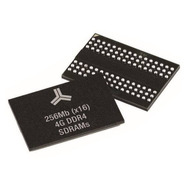
AS4C256M16D4
Revision History
4Gb DDR4 AS4C256M16D4 - 96 ball FBGA PACKAGE
Revision
Details
Date
Rev 1.0
Preliminary datasheet
Aug 2019
Alliance Memory Inc. 511 Taylor Way, San Carlos, CA 94070 TEL: (650) 610-6800 FAX: (650) 620-9211
Alliance Memory Inc. reserves the right to change products or specification without notice
Confidential
- 1 of 201 -
Rev.1.0 Aug.2019
�AS4C256M16D4
256M x 16 bit DDR4 Synchronous DRAM (SDRAM)
Advance (Rev. 1.0, Aug. /2019)
Features
Internal
JEDEC
Standard Compliant
Fast clock rate: 1200/1333MHz
Power supplies:
- VDD & VDDQ = +1.2V ± 0.06V
- VPP = +2.5V -0.125V / +0.25V
Operating
temperature range:
- Commercial : TC = 0~95°C
- Industrial: TC = -40~95°C
Supports
JEDEC clock jitter specification
Bidirectional
differential data strobe, DQS &DQS#
Differential Clock, CK & CK#
8 internal banks: 2 groups of 4 banks each
Separated IO gating structures by Bank Group
8n-bit prefetch architecture
Precharge & Active power down
Auto Refresh and Self Refresh
Low-power auto self refresh (LPASR)
Self Refresh Abort
Fine Granularity Refresh
Dynamic ODT (RTT_PARK & RTT_Nom & RTT_WR)
Write Leveling
DQ Training via MPR
Programmable preamble is supported both of 1tCK
and 2tCK mode
Command/Address (CA) Parity
Data bus write cyclic redundancy check (CRC)
Boundary Scan Mode
VREFDQ Training
Read Preamble Training
Control Gear Down Mode
Per DRAM Addressability (PDA)
Output Driver Impedance Control
Dynamic on-die termination (ODT)
Input Data Mask (DM) and Data Bus Inversion (DBI)
ZQ Calibration
Command/Address latency (CAL)
Asynchronous Reset
DLL enable/disable
Burst Length (BL8/BC4/BC4 or 8 on the fly)
Burst type: Sequential / Interleave
CAS Latency (CL)
CAS Write Latency (CWL)
Additive Latency (AL): 0, CL-1, CL-2
Average refresh period
- 8192 cycles/64ms (7.8us at -40°C ≤ TC ≤ +85°C)
- 8192 cycles/32ms (3.9us at +85°C ≤ TC ≤ +95°C)
Data
Interface: Pseudo Open Drain (POD)
compliant
Hard post package repair (hPPR)
Soft post package repair (sPPR)
Package: Pb Free and Halogen Free
RoHS
- 96-ball 7.5 x 13.5 x 1.2mm FBGA
Table 1. Ordering Information
Max Clock (MHz)
Package
Commercial (Extended)
0°C to 95°C
1200
96-ball FBGA
AS4C256M16D4-83BIN
256M x 16 Industrial -40°C to 95°C
1200
96-ball FBGA
AS4C256M16D4-75BCN
256M x 16
Commercial (Extended)
0°C to 95°C
1333
96-ball FBGA
AS4C256M16D4-75BIN
256M x 16 Industrial -40°C to 95°C
1333
96-ball FBGA
Product part No
Org
AS4C256M16D4-83BCN
256M x 16
Temperature
Table 2. Speed Grade Information
tRCD(ns)
Speed Grade
Clock Frequency
CAS Latency
DDR4-2400
1200 MHz
17
14.16
14.16
DDR4-2666
1333 MHz
19
14.25
14.25
Confidential
- 2 of 201 -
tRP(ns)
Rev.1.0 Aug.2019
�AS4C256M16D4
Ball Assignment
1
2
3
A
VDDQ
VSSQ
B
VPP
C
…
7
8
9
DQ8
UDQS#
VSSQ
VDDQ
VSS
VDD
UDQS
DQ9
VDD
VDDQ
DQ12
DQ10
DQ11
DQ13
VSSQ
D
VDD
VSSQ
DQ14
DQ15
VSSQ
VDDQ
E
VSS
UDM#/
UDBI#
VSSQ
LDM#/
LDBI#
VSSQ
VSS
F
VSSQ
VDDQ
LDQS#
DQ1
VDDQ
ZQ
G
VDDQ
DQ0
LDQS
VDD
VSS
VDDQ
H
VSSQ
DQ4
DQ2
DQ3
DQ5
VSSQ
J
VDD
VDDQ
DQ6
DQ7
VDDQ
VDD
K
VSS
CKE
ODT
CK
CK#
VSS
L
VDD
WE#/
A14
ACT#
CS#
RAS#/
A16
VDD
M
VREFCA
BG0
A10/AP
A12/
BC#
CAS#/
A15
VSS
N
VSS
BA0
A4
A3
BA1
TEN
P
Reset#
A6
A0
A1
A5
Alert#
R
VDD
A8
A2
A9
A7
VPP
T
VSS
A11
PAR
NC
A13
VDD
Figure 1. 96-Ball (FBGA Top View)
Confidential
- 3 of 201 -
Rev.1.0 Aug.2019
�AS4C256M16D4
Functional Block Diagram
Bank Group 0
CKE
CS#
RAS#/A16
CAS#/A15
WE#/A14
RESET#
PAR
TEN
ACT#
Row
Decoder
DLL
CLOCK
BUFFER
COMMAND
DECODER
Row
Decoder
CONTROL
SIGNAL
GENERATOR
COLUMN
COUNTER
A10/AP
A12/BC#
Row
Decoder
CK
CK#
32M x 16
CELL ARRAY
(BANK #0)
Column Decoder
32M x 16
CELL ARRAY
(BANK #1)
Column Decoder
32M x 16
CELL ARRAY
(BANK #2)
Column Decoder
Row
Decoder
ADDRESS
BUFFER
REFRESH
COUNTER
ZQ CAL
BG
BGand
& BA
BA
CONTROL
Control
BG0
BA0~BA1
LDQS
LDQS#
UDQS
UDQS#
Row
Decoder
RZQ
DATA
STROBE
BUFFER
DQ
Buffer
DQ0~DQ15
Row
Decoder
VSSQ
Row
Decoder
A0~A9
A11
A13
A14
Row
Decoder
MODE
REGISTER
ODT
ALERT#
CRC and
parity Control
LDM#/LDBI#
UDM#/UDBI#
32M x 16
CELL ARRAY
(BANK #3)
Column Decoder
32M x 16
CELL ARRAY
(BANK #0)
Column Decoder
32M x 16
CELL ARRAY
(BANK #1)
Column Decoder
32M x 16
CELL ARRAY
(BANK #2)
Column Decoder
32M x 16
CELL ARRAY
(BANK #3)
Column Decoder
Bank Group 1
Figure 2. Block Diagram
Confidential
- 4 of 201 -
Rev.1.0 Aug.2019
�AS4C256M16D4
Simplified State Diagram
This simplified State Diagram is intended to provide an overview of the possible state transitions and the
commands to control them. In particular, situations involving more than on bank, the enabling or disabling of
on-die termination, and some other events are not captured in full detail.
from any state
IVREFDQ,
RTT and
so on
RESET
SRX* = SRX with NOP
CKE_L
MRS
MRS, MPR,
Write Leveling
PDA
mode
RESET
N
ZQ
Calibration
ZQCL,ZQCS
CKE_L
Active
Power
Down
ACT = Active
PRE = Precharge
PREA = Precharge All
Idle
REF
ACT
E
PD DX
P
ZQCL
Connectivity
Test
Self
Refresh
VREFDQ training
S
MR S
MR
TE
Initialization
S
SR RE
X
RESET
Procedure
MRS
Power
On
TEN
Power applied
Precharge
Power
Down
Activating
PD
PD X
E
MRS = Mode Register Set
Refreshing
CKE_L
REF = Refresh, Fine granularity Refresh
Bank
Active
TEN = Boundary Scan Mode Enable
Read = RD, RDS4, RDS8
A
A
RE
AD
AD
W
E
RE
WRITE
Write = WR, WRS4, WRS8 with/without CRC
T
RI
WR
ITE
Read A = RDA, RDAS4, RDAS8
READ
Write A = WRA, WRAS4, WRAS8 with/without CRC
RESET = Start RESET procedure
Writing
PDE = Enter Power-down
READ
WRITE
Reading
PDX = Exit Power-down
SRE = Self-Refresh entry
SRX = Self-Refresh exit
MPR = Multi-Purpose Register
WRITE A
READ A
TE
RI
PDA = Per DRAM Addressability
AD
W
A
Reading
RE
A
,P
PR
E
EA
PR
PRE, PREA
E,
Writing
PR
Automatic Sequence
Command Sequence
RE
A
Precharging
Figure 3. State Diagram
Confidential
- 5 of 201 -
Rev.1.0 Aug.2019
�AS4C256M16D4
Ball Descriptions
Table 3. Ball Details
Symbol
Type
Description
CK, CK#
Input
CKE
Input
CS#
Input
Clock: CK and CK# are differential clock inputs. All control and address input
signals are sampled on the crossing of the positive edge of CK and the negative
edge of CK#.
Clock Enable: CKE high activates, and CKE low deactivates, internal clock signals
and device input buffers and output drivers. Taking CKE low provides Precharge
Power Down and Self-Refresh operation (all banks idle), or Active Power Down (row
Active in any bank). CKE is asynchronous for Self-Refresh exit. After VREFCA and
Internal DQ VREF have become stable during the power on and initialization sequence,
they must be maintained during all operations (including Self-Refresh). CKE must be
maintained high throughout read and write accesses. Input buffers, excluding CK,
CK#, ODT and CKE, are disabled during power down. Input buffers, excluding CKE,
are disabled during Self-Refresh.
Chip Select: All commands are masked when CS# is registered high. CS# provides
for external Rank selection on systems with multiple Ranks. CS# is considered part
of the command code.
ODT
Input
On Die Termination: ODT (registered high) enables RTT_NOM termination resistance
internal to the DDR4 SDRAM. When enabled, ODT is applied to each DQ, LDQS,
LDQS#, UDQS, UDQS#, LDM, and UDM signal. The ODT pin will be ignored if MR1
is programmed to disable RTT_NOM.
Activation Command Input: ACT# defines the Activation command being entered
along with CS#. The input into RAS#/A16, CAS#/A15 and WE#/A14 will be considered
as Row Address A16, A15 and A14.
RAS#/A16
Input Command Inputs: RAS#/A16, CAS#/A15 and WE#/A14 (along with CS#) define the
command being entered. Those pins have multi function. For example, for activation
CAS#/A15
with ACT# low, those are Addressing like A16, A15 and A14 but for non-activation
WE#/A14
command with ACT# high, those are Command pins for Read, Write and other
command defined in command truth table.
LDM#/LDBI# Input / Input Data Mask and Data Bus Inversion: DM# is an input mask signal for write
data. Input data is masked when DM# is sampled low coincident with that input data
UDM#/UDBI# Output
during a Write access. DM# is sampled on both edges of DQS. DM is muxed with
DBI function by Mode Register A10, A11, A12 setting in MR5. DBI# is an input
/output identifying whether to store/output the true or inverted data. If DBI# is low the
data will be stored/output after inversion inside the DDR4 SDRAM and not inverted if
DBI# is high.
BG0
Input Bank Group Inputs: BG0 define to which bank group an Active, Read, Write or
Precharge command is being applied. BG0 also determines which mode register is
to be accessed during a MRS cycle.
BA0-BA1
Input Bank Address: BA0-BA1 define to which bank an Active, Read, Write, or Precharge
command is being applied. Bank address also determines which mode register is to
be accessed during a MRS cycle.
A0-A16
Input Address Inputs: Provide the row address for Activate Commands and the column
address for Read/Write commands to select one location out of the memory array in
the respective bank. (A10/AP, A12/BC#, RAS#/A16, CAS#/A15 and WE#/A14 have
additional functions, see other rows. The address inputs also provide the op-code
during Mode Register Set commands. A15 and A16 are used on some higher densities.
A10/AP
Input Auto-precharge: A10 is sampled during Read/Write commands to determine whether
Autoprecharge should be performed to the accessed bank after the Read/Write
operation. (high: Autoprecharge; low: no Autoprecharge). A10 is sampled during a
Precharge command to determine whether the Precharge applies to one bank (A10
low) or all banks (A10 high). If only one bank is to be precharged, the bank is selected
by bank addresses.
ACT#
Confidential
Input
- 6 of 201 -
Rev.1.0 Aug.2019
�AS4C256M16D4
A12/BC#
Input
Reset#
Input
DQ0-DQ15
Input /
Output
LDQS,
LDQS#,
UDQS,
UDQS#,
Input /
Output
PAR
Input
Alert#
Input /
Output
TEN
Input
NC
-
Burst Chop: A12/BC# is sampled during Read and Write commands to determine if
burst chop (on-the-fly) will be performed. (high, no burst chop; low: burst chopped).
See command truth table for details.
Active Low Asynchronous Reset: Reset is active when Reset# is low, and inactive
when Reset# is high. Reset# must be high during normal operation. Reset# is a
CMOS rail-to-rail signal with DC high and low at 80% and 20% of VDD.
Data Input/ Output: Bi-directional data bus. If CRC is enabled via Mode register
then CRC code is added at the end of Data Burst. Any DQ from DQ0~DQ3 may
indicate the internal VREF level during test via Mode Register Setting MR4 A4=high.
During this mode, RTT should be set Hi-Z.
Data Strobe: output with read data, input with write data. Edge-aligned with read
data, centered in write data. LDQS corresponds to the data on DQ0-DQ7; UDQS
corresponds to the data on DQ8-DQ15. The data strobe LDQS and UDQS are
paired with differential signals LDQS#, and UDQS#, respectively, to provide
differential pair signaling to the system during reads and writes. DDR4 SDRAM
supports differential data strobe only and does not support single-ended.
Command and Address Parity Input: DDR4 Supports Even Parity check in DRAM
with MR setting. Once it’s enabled via Register in MR5, then DRAM calculates Parity
with ACT#, RAS#/A16, CAS#/A15, WE#/A14, BG0, BA0-BA1, and A16-A0. Command
and address inputs shall have parity check performed when commands are latched
via the rising edge of CK and when CS# is low.
Alert: It has multi functions such as CRC error flag, Command and Address Parity
error flag as Output signal. If there is error in CRC, then Alert# goes low for the
period time interval and goes back high. If there is error in Command Address Parity
Check, then Alert# goes low for relatively long period until ongoing DRAM internal
recovery transaction to complete. During Connectivity Test mode, this pin works as
input. Using this signal or not is dependent on system. In case of not connected as
Signal, Alert# Pin must be bounded to VDD on board.
Connectivity Test Mode Enable: Connectivity Test Mode is active when TEN is
high, and inactive when TEN is low. TEN must be low during normal operation. TEN
is a CMOS rail-to-rail signal with AC high and low at 80% and 20% of VDD (960mV
for DC high and 240mV for DC low). Using this signal or not is dependent on
System. This pin may be DRAM internally pulled low through a weak pull-down
resistor to VSS.
No Connect: These pins should be left unconnected.
VDD
Supply Power Supply: +1.2V 0.06V.
VSS
Supply Ground
VDDQ
Supply DQ Power Supply: +1.2V 0.06V.
VSSQ
Supply DQ Ground
VPP
Supply DRAM Activating Power Supply: 2.5V ( 2.375V min , 2.75V max)
VREFCA
ZQ
Supply Reference voltage for CA
Supply Reference pin for ZQ calibration.
NOTE: Input only pins (BG0, BA0-BA1, A0-A16, ACT#, RAS#/A16, CAS#/A15, WE#/A14, CS#, CKE, ODT, and RESET#) do not supply termination.
Confidential
- 7 of 201 -
Rev.1.0 Aug.2019
�AS4C256M16D4
Basic Functionality
The DDR4 SDRAM is a high-speed dynamic random-access memory internally organized with eight-banks
(2 bank groups each with 4 banks). The DDR4 SDRAM uses a 8n prefetch architecture to achieve high-speed
operation. The 8n prefetch architecture is combined with an interface designed to transfer two data words per
clock cycle at the I/O pins. A single read or write operation for the DDR4 SDRAM consists of a single 8n-bit
wide, four clock data transfer at the internal DRAM core and eight corresponding n-bit wide, one-half clock
cycle data transfers at the I/O pins.
Read and write operation to the DDR4 SDRAM are burst oriented, start at a selected location, and continue
for a burst length of eight or a ‘chopped’ burst of four in a programmed sequence. Operation begins with the
registration of an Activate Command, which is then followed by a Read or Write command. The address bits
registered coincident with the Activate Command are used to select the bank and row to be activated (BG0
select the bank group; BA0-BA1 select the bank; A0-A14 select the row). The address bits registered
coincident with the Read or Write command are used to select the starting column location for the burst
operation, determine if the auto precharge command is to be issued (via A10), and select BC4 or BL8 mode
‘on the fly’ (via A12) if enabled in the mode register.
Prior to normal operation, the DDR4 SDRAM must be powered up and initialized in a predefined manner.
The following sections provide detailed information covering device reset and initialization, register definition,
command descriptions, and device operation.
Reset and Initialization Procedure
For power-up and reset initialization, in order to prevent DRAM from functioning improperly, default values
for the following MR settings need to be defined:
Gear down mode (MR3 A[3]) : 0 = 1/2 Rate
Per DRAM Addressability (MR3 A[4]) : 0 = Disable
CS# to Command/Address Latency (MR4 A[8:6]) : 000 = Disable
CA Parity Latency Mode (MR5 A[2:0]) : 000 = Disable
Hard Post Package Repair mode (MR4 A[13]) : 0 = Disable
Soft Post Package Repair mode (MR4 A[5]) : 0 = Disable
Power-up Initialization Sequence
The following sequence is required for Power up and Initialization:
1. Apply power (Reset# and TEN are recommended to be maintained below 0.2 x V DD; all other inputs may be
undefined). Reset# needs to be maintained below 0.2 x VDD for minimum 200us with stable power and TEN
needs to be maintained below 0.2 x VDD for minimum 700us with stable power. CKE is pulled “Low” anytime
before Reset# being de-asserted (min. time 10ns). The power voltage ramp time between 300mV to VDD,min
must be no greater than 200ms; and during the ramp, VDD ≥ VDDQ and (VDD-VDDQ) < 0.3 V. VPP must ramp at
the same time or earlier than VDD and VPP must be equal to or higher than VDD at all times.
During power-up, either of the following conditions may exist and must be met:
Condition A:
VDD and VDDQ are driven from a single power converter output, AND
The voltage levels on all pins other than VDD, VDDQ, VSS, VSSQ must be less than or equal to VDDQ and VDD
on one side and must be larger than or equal to VSSQ and VSS on the other side. In addition, VTT is limited
to 0.76 V max once power ramp is finished, AND
VREFCA tracks VDD/2.
Condition B:
Apply VDD without any slope reversal before or at the same time as V DDQ
Apply VDDQ without any slope reversal before or at the same time as V TT & VREFCA.
Apply VPP without any slope reversal before or at the same time as V DD.
The voltage levels on all pins other than VDD, VDDQ, VSS, VSSQ must be less than or equal to VDDQ and VDD
on one side and must be larger than or equal to VSSQ and VSS on the other side.
2. After Reset# is de-asserted, wait for another 500us until CKE becomes active. During this time, the DRAM
will start internal initialization; this will be done independently of external clocks.
Confidential
- 8 of 201 -
Rev.1.0 Aug.2019
�AS4C256M16D4
3. Clocks (CK, CK#) need to be started and stabilized for at least 10ns or 5t CK (which is larger) before CKE
goes active. Since CKE is a synchronous signal, the corresponding setup time to clock (t IS) must be met.
Also a Deselect command must be registered (with tIS set up time to clock) at clock edge Td. Once the CKE
registered “high” after Reset, CKE needs to be continuously registered “high” until the initialization sequence
is finished, including expiration of tDLLK and tZQinit.
4. The DDR4 SDRAM keeps its on-die termination in high-impedance state as long as Reset# is asserted.
Further, the SDRAM keeps its on-die termination in high impedance state after Reset# deassertion until
CKE is registered high. The ODT input signal may be in undefined state until tIS before CKE is registered
high. When CKE is registered high, the ODT input signal may be statically held at either low or high. If RTT_NOM
is to be enabled in MR1 the ODT input signal must be statically held low. In all cases, the ODT input signal
remains static until the power up initialization sequence is finished, including the expiration of tDLLK and tZQinit.
5. After CKE is being registered high, wait minimum of Reset CKE Exit time, t XPR, before issuing the first MRS
command to load mode register. (tXPR=Max(tXS, 5nCK)]
6. Issue MRS Command to load MR3 with all application settings (To issue MRS command to MR3, provide
“ low” to BG0, “high” to BA1, BA0)
7. Issue MRS command to load MR6 with all application settings (To issue MRS command to MR6, provide
“low” to BA0, “high” to BG0, BA1)
8. Issue MRS command to load MR5 with all application settings (To issue MRS command to MR5, provide
“low” to BA1, “high” to BG0, BA0)
9. Issue MRS command to load MR4 with all application settings (To issue MRS command to MR4, provide
“Low” to BA1, BA0, “High” to BG0)
10. Issue MRS command to load MR2 with all application settings (To issue MRS command to MR2, provide
“Low” to BG0, BA0, “High” to BA1)
11. Issue MRS command to load MR1 with all application settings (To issue MRS command to MR1, provide
“Low” to BG0, BA1, “High” to BA0)
12. Issue MRS command to load MR0 with all application settings (To issue MRS command to MR0, provide
“Low” to BG0, BA1, BA0)
13. Issue ZQCL command to starting ZQ calibration.
14. Wait for both tDLLK and tZQinit completed.
15. The DDR4 SDRAM is now ready for Read/Write training (include VREF training and Write leveling).
CK#
CK
Ta
Tb
Tc
Td
Te
Tf
Tg
Th
Ti
Tj
Tk
tCKSRX
VPP
VDD,VDDQ
200μs
500μs
RESET#
CKE
tIS
10ns
VALID
tIS
CMD
tDLLK
Note 1
BA
tXPR
tMRD
tMRD
tMRD
tZQinit
tMOD
MRS
MRS
MRS
MRS
MRx
MRx
MRx
MRx
ZQCL
Note 1
VALID
tIS
ODT
VALID
tIS
Static LOW in case RTT_NOM is enabled at time Tg, otherwise static HIGH or LOW
VALID
RTT
NOTE 1. From time point "Td" until "Tk " DES commands must be applied between MRS and ZQCL commands.
NOTE 2. MRS Commands must be issued to all Mode Registers that have defined settings.
TIME BREAK
DON'T CARE
Figure 4. RESET# and Initialization Sequence at Power-on Ramping
Confidential
- 9 of 201 -
Rev.1.0 Aug.2019
�AS4C256M16D4
VDD Slew rate at Power-up Initialization Sequence
Table 4. VDD
Slew Rate
Symbol
Min.
Max.
Units
Notes
VDD_sl
0.004
600
V/ms
1,2
VDD_ona
-
200
ms
3
Notes:
1. Measurement made between 300mv and 80% VDD minimum.
2. 20 MHz bandlimited measurement.
3. Maximum time to ramp VDD from 300 mv to VDD minimum.
Reset Initialization with Stable Power
The following sequence is required for Reset at no power interruption initialization:
1. Asserted Reset# below 0.2 x VDD anytime when reset is needed (all other inputs may be undefined). Reset#
needs to be maintained for minimum tPW_Reset. CKE is pulled "low" before Reset# being de-asserted (min.
time 10 ns).
2. Follow steps 2 to 10 in “Power-up Initialization Sequence”.
3. The Reset sequence is now completed, DDR4 SDRAM is ready for Read/Write training (include VREF
training and Write leveling)
CK#
CK
Ta
Tb
Tc
Td
Te
Tf
Tg
Th
Ti
Tj
Tk
tCKSRX
VPP
VDD,VDDQ
tPW_Reset
500μs
RESET#
CKE
10ns
VALID
tIS
CMD
tDLLK
tIS
Note 1
BA
tXPR
tMRD
tMRD
tMRD
tZQinit
tMOD
MRS
MRS
MRS
MRS
MRx
MRx
MRx
MRx
ZQCL
Note 1
VALID
tIS
ODT
VALID
tIS
Static LOW in case RTT_NOM is enabled at time Tg, otherwise static HIGH or LOW
VALID
RTT
NOTE 1. From time point "Td" until "Tk " DES commands must be applied between MRS and ZQCL commands.
NOTE 2. MRS Commands must be issued to all Mode Registers that have defined settings.
TIME BREAK
DON'T CARE
Figure 5. Reset Procedure at Power Stable
Confidential
- 10 of 201 -
Rev.1.0 Aug.2019
�AS4C256M16D4
Operation Mode Truth Table
Notes 1, 2, 3 and 4 apply to the entire Command Truth Table.
Note 5 Applies to all Read/Write commands.
[BG=Bank Group Address, BA=Bank Address, RA=Row Address, CA=Column Address, BC#=Burst Chop, X=Don’t Care, V=Valid].
Table 5. Command Truth Table
Function
Mode Register Set
Symbol CKEn-1 CKEn
CS# ACT#
RAS# CAS# WE#/
/A16 /A15 A14
BG0 BA0-1
BC#/
A12
A13,
A11
A10/
A0-A9
AP
MRS
H
H
L
H
L
L
L
BG
BA
Refresh
OP Code
REF
H
H
L
H
L
L
H
V
V
V
V
V
V
Self Refresh Entry 7,9
SRE
H
L
L
H
L
L
H
V
V
V
V
V
V
H
X
X
X
X
X
X
X
X
X
X
Self Refresh Exit 7-10
SRX
L
H
L
H
H
H
H
V
V
V
V
V
V
Single Bank Precharge
PRE
H
H
L
H
L
H
L
BG
BA
V
V
L
V
PREA
H
H
L
H
L
H
L
V
V
V
V
H
V
RFU
RFU
H
H
L
H
L
H
H
RFU
RFU
RFU
RFU
RFU
RFU
Bank Activate
ACT
H
H
L
L
RA
RA
RA
BG
BA
RA
RA
RA
RA
Write (Fixed BL8 or BC4)
WR
H
H
L
H
H
L
L
BG
BA
V
V
L
CA
Write (BC4, on the Fly)
WRS4
H
H
L
H
H
L
L
BG
BA
L
V
L
CA
Write (BL8, on the Fly)
WRS8
H
H
L
H
H
L
L
BG
BA
H
V
L
CA
Write with Auto Precharge
(Fixed BL8 or BC4)
WRA
H
H
L
H
H
L
L
BG
BA
V
V
H
CA
WRAS4
H
H
L
H
H
L
L
BG
BA
L
V
H
CA
WRAS8
H
H
L
H
H
L
L
BG
BA
H
V
H
CA
Precharge all Banks
Write with Auto Precharge
(BC4, on the Fly)
Write with Auto Precharge
(BL8, on the Fly)
Read (Fixed BL8 or BC4)
RD
H
H
L
H
H
L
H
BG
BA
V
V
L
CA
Read (BC4, on the Fly)
RDS4
H
H
L
H
H
L
H
BG
BA
L
V
L
CA
Read (BL8, on the Fly)
RDS8
H
H
L
H
H
L
H
BG
BA
H
V
L
CA
RDA
H
H
L
H
H
L
H
BG
BA
V
V
H
CA
RDAS4
H
H
L
H
H
L
H
BG
BA
L
V
H
CA
RDAS8
H
H
L
H
H
L
H
BG
BA
H
V
H
CA
No Operation
NOP
H
H
L
H
H
H
H
V
V
V
V
V
V
Device Deselected
DES
H
H
H
X
X
X
X
X
X
X
X
X
X
Read with Auto Precharge
(Fixed BL8 or BC4)
Read with Auto Precharge
(BC4, on the Fly)
Read with Auto Precharge
(BL8, on the Fly)
Power Down Entry
6
PDE
H
L
H
X
X
X
X
X
X
X
X
X
X
Power Down Exit 6
PDX
L
H
H
X
X
X
X
X
X
X
X
X
X
ZQ calibration Long
ZQCL
H
H
L
H
H
H
L
V
V
V
V
H
V
ZQ calibration Short
ZQCS
H
H
L
H
H
H
L
V
V
V
V
L
V
Note 1. All DDR4 SDRAM commands are defined by states of CS#, ACT#, RAS#/A16, CAS#/A15, WE#/A14 and CKE at the rising edge of the clock. The
MSB of BG, BA, RA and CA are device density and configuration dependent. When ACT# = H; pins RAS#/A16, CAS#/A15, and WE#/A14 are used
as command pins RAS#, CAS#, and WE# respectively. When ACT# = L; pins RAS#/A16, CAS#/A15, and WE#/A14 are used as address pins A16,
A15, and A14 respectively.
Note 2. Reset# is low enable command which will be used only for asynchronous reset so must be maintained high during any function.
Note 3. Bank Group addresses (BG) and Bank addresses (BA) determine which bank within a bank group to be operated upon. For MRS commands the BG
and BA selects the specific Mode Register location.
Note 4. “V” means “H or L (but a defined logic level)” and “X” means either “defined or undefined (like floating) logic level”.
Note 5. Burst reads or writes cannot be terminated or interrupted and Fixed/on-the-Fly BL will be defined by MRS.
Note 6. The Power Down Mode does not perform any refresh operation.
Note 7. The state of ODT does not affect the states described in this table. The ODT function is not available during Self Refresh.
Note 8. Controller guarantees self refresh exit to be synchronous.
Note 9. VPP and VREF(VREFCA) must be maintained during Self Refresh operation.
Note 10. The No Operation (NOP) command may be used only when entering gear-down mode.
Note 11. Refer to the CKE Truth Table for more detail with CKE transition.
Confidential
- 11 of 201 -
Rev.1.0 Aug.2019
�AS4C256M16D4
Table 6. CKE Truth Table
CKEn-1 (1)
CKEn (1)
L
L
Command n (3)
RAS#, CAS#, WE#, CS#
X
L
H
L
L
L
Bank(s) Active
Reading
Current State (2)
Action n (3)
Notes
Maintain Power-Down
14,15
Deselect
Power-Down Exit
11,14
X
Maintain Self-Refresh
15,16
H
Deselect
Self-Refresh Exit
8,12,16
H
L
Deselect
Active Power-Down Entry
11,13,14
H
L
Deselect
Power-Down Entry
11,13,14,17
Writing
H
L
Deselect
Power-Down Entry
11,13,14,17
Precharging
H
L
Deselect
Power-Down Entry
11,13,14,17
Refreshing
H
L
Deselect
Precharge Power-Down Entry
11
H
L
Deselect
Precharge Power-Down Entry
11,13,14,18
L
Refresh
Self-Refresh
9,13,18
Power-Down
Self-Refresh
All Banks Idle
H
See Command Truth Table for additional command details
10
Notes:
1. CKEn is the logic state of CKE at clock edge n; CKEn-1 was the state of CKE at the previous clock edge.
2. Current state is defined as the state of the DDR4 SDRAM immediately prior to clock edge n.
3. Command n is the command registered at clock edge n, and Action n is a result of command n, ODT is not included here.
4. All states and sequences not shown are illegal or reserved unless explicitly described elsewhere in this document.
5. The state of ODT does not affect the states described in this table. The ODT function is not available during Self Refresh.
6. During any CKE transition (registration of CKE H → L or CKE L → H) the CKE level must be maintained until 1nCK prior to tCKEmin being
satisfied (at which time CKE may transition again).
7. Deselect and NOP are defined in the Command Truth Table.
8. On Self Refresh Exit Deselect commands must be issued on every clock edge occurring during the tXS period. Read or ODT commands
may be issued only after tXSDLL is satisfied.
9. Self Refresh mode can only be entered from the All Banks Idle state.
10. Must be a legal command as defined in the Command Truth Table.
11. Valid commands for Power Down Entry and Exit are Deselect only.
12. Valid commands for Self Refresh Exit are Deselect only. except for Gear Down mode. NOP is allowed for the mode.
13. Self Refresh cannot be entered during Read or Write operations. For a detailed list of restrictions see section “Self-Refresh Operation”
and see section “Power-Down Modes”.
14. The Power Down does not perform any refresh operations.
15. “X” means “don't care” (including floating around VREF) in Self Refresh and Power Down. It also applies to Address pins.
16. VPP and VREF (VREFCA) must be maintained during Self Refresh operation.
17. If all banks are closed at the conclusion of the read, write or precharge command, then Precharge Power Down is entered, otherwise
Active Power Down is entered.
18. ‘Idle state’ is defined as all banks are closed (tRP, tDAL, etc. satisfied), no data bursts are in progress, CKE is high, and all timings from
previous operations are satisfied (tMRD, tMOD, tRFC, tZQinit, tZQoper, tZQCS, etc.) as well as all Self Refresh exit and Power Down Exit
parameters are satisfied (tXS, tXP, etc).
Confidential
- 12 of 201 -
Rev.1.0 Aug.2019
�AS4C256M16D4
Programming the Mode Registers
For application flexibility, various functions, features, and modes are programmable in seven Mode Registers,
provided by the DDR4 SDRAM, as user defined variables and they must be programmed via a Mode Register
Set (MRS) command. The mode registers are divided into various fields depending on the functionality and/or
modes. As not all the Mode Registers (MRn) have default values defined, contents of Mode Registers must be
initialized and/or re-initialized, i.e. written, after power up and/or reset for proper operation. Also the contents of
the Mode Registers can be altered by re-executing the MRS command during normal operation. When
programming the mode registers, even if the user chooses to modify only a sub-set of the MRS fields, all
address fields within the accessed mode register must be redefined when the MRS command is issued. MRS
command and DLL Reset do not affect array contents, which means these commands can be executed any
time after power-up without affecting the array contents. MRS Commands can be issued only when DRAM is
at idle state. The mode register set command cycle time, tMRD is required to complete the write operation to the
mode register and is the minimum time required between two MRS commands shown in the tMRD timing figure.
T0
T1
T2
Ta0
Ta1
Ta2
Tb0
Tb1
CMD
VALID
VALID
VALID
MRS2
DES
DES
DES
ADDR
VALID
VALID
VALID
VALID
VALID
VALID
VALID
CK#
CK
CKE
Tb2
Tb3
Tb4
MRS
DES
DES
DES
VALID
VALID
VALID
VALID
tMRD
Old Settings
Settings
Updating Settings
NOTE 1. This timing diagram shows C/A Parity Latency mode is “Disable” case.
NOTE 2. List of MRS commands exception that do not apply to tMRD
- Gear down mode
- C/A Parity Latency mode
- CS to Command/Address Latency mode
- Per DRAM Addressability mode
- VREFDQ training Value, VREFDQ Training mode and VREFDQ training Range.
TIME BREAK
DON'T CARE
Figure 6. tMRD timing
Some of the Mode Register setting affect to address/command/control input functionality. These case, next
MRS command can be allowed when the function updating by current MRS command completed.
The MRS commands that do not apply tMRD timing to next MRS command. These MRS command input
cases have unique MR setting procedure, so refer to individual function description.
Confidential
- 13 of 201 -
Rev.1.0 Aug.2019
�AS4C256M16D4
The most MRS command to Non-MRS command delay, tMOD, is required for the DRAM to update the features,
and is the minimum time required from an MRS command to a non-MRS command excluding DES, as shown
in the tMOD timing figure.
Some of the mode register setting cases, function updating takes longer than tMOD. The MRS commands that
do not apply tMOD timing to next valid command excluding DES is listed in Note 2 of tMOD timing figure. These
MRS command input cases have unique MR setting procedure, so refer to individual function description.
T0
T1
Ta0
CMD
VALID
VALID
ADDR
VALID
VALID
Ta1
Ta2
Ta3
Ta4
Tb0
Tb1
Tb2
Tb3
MRS2
DES
DES
DES
DES
DES
VALID
VALID
VALID
VALID
VALID
VALID
VALID
VALID
VALID
VALID
VALID
VALID
CK#
CK
CKE
tMOD
Old Settings
Settings
Updating Settings
NOTE 1. This timing diagram shows C/A Parity Latency mode is “Disable” case.
NOTE 2. List of MRS commands exception that do not apply to tMOD
- DLL Enable, DLL Reset
- VREFDQ training Value, internal VREF Monitor, VREFDQ Training mode and VREFDQ training Range
- Gear down mode
- Per DRAM addressability mode
- CA Parity mode
New Settings
TIME BREAK
DON'T CARE
Figure 7. tMOD timing
CK#
CK
CMD
MRS
DODTLoff + 1
ODT
tMOD
tADC_min
tADC_min
RTT_NOM
RTT
RTT_NOM
tADC_max
tADC_max
NOTE 1. This timing diagram shows C/A Parity Latency mode is “Disable” case.
NOTE 2. When an MRS command mentioned in this note affects RTT_NOM turn on timings, RTT_NOM turn off timings and RTT_NOM value,
this means the MR register value changes. The ODT signal should set to be low for at least DODTLoff +1 clock before their affecting
MRS command is issued and remain low until tMOD expires. The following MR registers affects RTT_NOM turn on timings, RTT_NOM turn off
timings and RTT_NOM value and it requires ODT to be low when an MRS command change the MR register value. If there are no change
the MR register value that correspond to commands mentioned in this note, then ODT signal is not require to be low.
- DLL control for precharge power down
- Additive latency and CAS read latency
- DLL enable and disable
- CAS write latency
- CA Parity mode
- Gear down mode
- RTT_NOM
Figure 8. ODT Status at MRS affecting ODT turn-on/off timing
The mode register contents can be changed using the same command and timing requirements during normal
operation as long as the device is in idle state, i.e., all banks are in the precharged state with t RP satisfied, all
data bursts are completed and CKE is high prior to writing into the mode register. If RTT_NOM function is intended
to change (enable to disable and vice versa) or already enabled in DRAM MR, ODT signal must be registered
Low ensuring RTT_NOM is in an off state prior to MRS command affecting RTT_NOM turn-on and off timing. The
ODT signal may be registered high after tMOD has expired. ODT signal is a don’t care during MRS command if
DRAM RTT_NOM function is disabled in the mode register prior and after an MRS command.
Confidential
- 14 of 201 -
Rev.1.0 Aug.2019
�AS4C256M16D4
Mode Register MR0
Table 7. MR0 Definition
BG0
BA1
BA0
0
0
0
A8
RAS# CAS# WE#/
A13
/A16 /A15 A14
0
0
A12
0*1
0
0*1
A11
A10
A9
WR & RTP*2,3
A8
A7
DLL
Rst
TM
A6
A5
A4
CL
A3
A2
BT
CL
A1
A0
BL
DLL Reset
A7
Test Mode
A3
Read Burst Type
A1
A0
BL
0
No
0
Normal
0
Sequential
0
0
8 (Fixed)
1
Yes
1
Interleave
0
1
BC4 or 8 (on the fly)
1
0
BC4 (Fixed)
1
1
Reserved
A11
A10
A9
WR
RTP
A6
A5
A4
A2
CAS Latency
0
0
0
10
5
0
0
0
0
9
6
10
0
0
1
12
0
0
0
1
0
1
0
14
7
0
0
1
0
11
0
1
1
16
8
0
0
1
1
12
1
0
0
18
9
0
1
0
0
13
1
0
1
20
10
0
1
0
1
14
0
1
1
0
15
0
1
1
1
1
0
1
1
16
17
Write Recovery and Read to Precharge for auto precharge
Note 1. Reserved for future use and must be programmed to 0 during MR.
Note 2. WR (write recovery for autoprecharge)min in clock cycles is calculated following rounding algorithm. The WR value in the mode
register must be programmed to be equal or larger than WRmin. The programmed WR value is used with tRP to determine tDAL.
Note 3. The table shows the encodings for Write Recovery and internal Read command to Precharge command delay. For actual Write
recovery timing, please refer to AC timing table.
CAS Latency
The CAS latency (CL) setting is defined in the MR0 Register Definition table. CAS latency is the delay, in
clock cycles, between the internal read command and the availability of the first bit of output data. The device
does not support half-clock latencies. The overall read latency (RL) is defined as additive latency (AL) + CAS
latency (CL): RL = AL + CL.
Test Mode
The normal operating mode is selected by MR0[7] and all other bits set to the desired values shown in the
MR0 Register Definition table. Programming MR0[7] to a value of 1 places the device into a DRAM
manufacturer-defined test mode to be used only by the manufacturer, not by the end user. No operations or
functionality is specified if MR0[7] = 1.
DLL Reset
The DLL reset bit is self-clearing, meaning that it returns to the value of 0 after the DLL reset function has
been issued. After the DLL is enabled, a subsequent DLL reset should be applied. Any time the DLL reset function
is used, tDLLK must be met before functions requiring the DLL can be used. (For example, Read commands or
ODT synchronous operations).
Confidential
- 15 of 201 -
Rev.1.0 Aug.2019
�AS4C256M16D4
Burst Length, Type and Order
Accesses within a given burst may be programmed to sequential or interleaved order. The burst type is
selected via bit A3 of Mode Register MR0. The ordering of accesses within a burst is determined by the burst
length, burst type, and the starting column address as shown in the following table. The burst length is defined
by bits A0-A1 of Mode Register MR0. Burst length options include fixed BC4, fixed BL8, and ‘on the fly’ which
allows BC4 or BL8 to be selected coincident with the registration of a Read or Write command via A12/BC#.
Table 8. Burst Type and Burst Order
Burst Length
4 Chop
Read/Write
Read
Write
8
Read
Starting Column Address
A2
0
0
0
0
1
1
1
1
0
1
0
0
0
0
1
1
1
1
V
A1
0
0
1
1
0
0
1
1
V
V
0
0
1
1
0
0
1
1
V
A0
0
1
0
1
0
1
0
1
V
V
0
1
0
1
0
1
0
1
V
Burst type = Sequential
(decimal) A3=0
burst type = Interleaved
(decimal) A3=1
0, 1, 2, 3, T, T, T, T
1, 2, 3, 0, T, T, T, T
2, 3, 0, 1, T, T, T, T
3, 0, 1, 2, T, T, T, T
4, 5, 6, 7, T, T, T, T
5, 6, 7, 4, T, T, T, T
6, 7, 4, 5, T, T, T, T
7, 4, 5, 6, T, T, T, T
0, 1, 2, 3, X, X, X, X
4, 5, 6, 7, X, X, X, X
0, 1, 2, 3, 4, 5, 6, 7
1, 2, 3, 0, 5, 6, 7, 4
2, 3, 0, 1, 6, 7, 4, 5
3, 0, 1, 2, 7, 4, 5, 6
4, 5, 6, 7, 0, 1, 2, 3
5, 6, 7, 4, 1, 2, 3, 0
6, 7, 4, 5, 2, 3, 0, 1
7, 4, 5, 6, 3, 0, 1, 2
0, 1, 2, 3, 4, 5, 6, 7
0, 1, 2, 3, T, T, T, T
1, 0, 3, 2, T, T, T, T
2, 3, 0, 1, T, T, T, T
3, 2, 1, 0, T, T, T, T
4, 5, 6, 7, T, T, T, T
5, 4, 7, 6, T, T, T, T
6, 7, 4, 5, T, T, T, T
7, 6, 5, 4, T, T, T, T
0, 1, 2, 3, X, X, X, X
4, 5, 6, 7, X, X, X, X
0, 1, 2, 3, 4, 5, 6, 7
1, 0, 3, 2, 5, 4, 7, 6
2, 3, 0, 1, 6, 7, 4, 5
3, 2, 1, 0, 7, 6, 5, 4
4, 5, 6, 7, 0, 1, 2, 3
5, 4, 7, 6, 1, 0, 3, 2
6, 7, 4, 5, 2, 3, 0, 1
7, 6, 5, 4, 3, 2, 1, 0
0, 1, 2, 3, 4, 5, 6, 7
Note
1, 2, 3
1, 2, 4,
5
2
Write
2, 4
Notes:
1. In case of burst length being fixed to 4 by MR0 setting, the internal write operation starts two clock cycles earlier than for the BL8 mode.
This means that the starting point for tWR and tWTR will be pulled in by two clocks. In case of burst length being selected on-the-fly via
A12/BC#, the internal write operation starts at the same point in time like a burst of 8 write operation. This means that during on-the-fly
control, the starting point for tWR and tWTR will not be pulled in by two clocks.
2. 0...7 bit number is value of CA[2:0] that causes this bit to be the first read during a burst.
3. T: Output driver for data and strobes are in high impedance.
4. V: a valid logic level (0 or 1), but respective buffer input ignores level on input pins.
5. X: Don’t Care.
Write Recovery (WR)/Read-to-Precharge (RTP)
The programmed write recovery (WR) value is used for the auto precharge feature along with tRP to determine
tDAL. WR for auto precharge (MIN) in clock cycles is calculated by dividing tWR (in ns) by tCK (in ns) and rounding
to the next integer:
The WR value must be programmed to be equal to or larger than tWR (MIN). When both DM and write CRC
are enabled in the mode register, the device calculates CRC before sending the write data into the array; tWR
values will change when enabled. If there is a CRC error, the device blocks the Write operation and discards
the data.
Internal Read-to-Precharge (RTP) command delay for auto precharge (MIN) in clock cycles is calculated by
dividing tRTP (in ns) by tCK (in ns) and rounding to the next integer:
The RTP value in the mode register must be programmed to be equal to or larger than RTP (MIN). The
programmed RTP value is used with tRP to determine the ACT timing to the same bank.
Confidential
- 16 of 201 -
Rev.1.0 Aug.2019
�AS4C256M16D4
Mode Register MR1
Table 9. MR1 Definition
BG0
BA1
BA0
0
0
1
A12
RAS# CAS# WE#/
A13
/A16 /A15 A14
0
0
Qoff
0*1
0
A7
A12
A11
Qoff*2
0*1
Write Leveling Enable
A10
A9
A8
RTT_NOM
A0
A7
A6
A5
WL
0*1
0*1
DLL Enable
*3
0
Output buffer enabled
0
Disable
0
Disable
1
Output buffer disabled
1
Enable
1
Enable
A4
A3
A2
AL*4
A1
ODI
A1
Output Driver Impedance Control
0
0
RZQ/7
0
1
RZQ/5
1
0
Reserved
1
1
Reserved
A9
A8
RTT_NOM
A4
A3
Additive Latency
0
0
0
RTT_NOM Disable
0
0
0(AL disabled)
0
0
1
RZQ/4
0
1
CL-1
0
1
0
RZQ/2
1
0
CL-2
0
1
1
RZQ/6
1
1
Reserved
1
0
0
1
0
1
RZQ/5
1
1
0
RZQ/3
1
1
1
RZQ/7
DLL
A2
A10
RZQ/1
A0
Note 1. Reserved for future use and must be programmed to 0 during MRS.
Note 2. Outputs disabled - DQs, DQSs, DQS#s.
Note 3. States reversed to “0 as Disable” with respect to DDR4.
Note 4. Additive Latency is not supported for x16 device.
DLL Enable/DLL Disable
The DLL must be enabled for normal operation and is required during power-up initialization and upon
returning to normal operation after having the DLL disabled. During normal operation (DLL enabled with
MR1[0]) the DLL is automatically disabled when entering the Self Refresh operation and is automatically reenabled upon exit of the Self Refresh operation. Any time the DLL is enabled and subsequently reset, tDLLK
clock cycles must occur before a Read or Synchronous ODT command can be issued to allow time for the
internal clock to be synchronized with the external clock. Failing to wait for synchronization to occur may result
in a violation of the tDQSCK, tAON, or tAOF parameters.
During tDLLK, CKE must continuously be registered High. The device does not require DLL for any Write
operation, except when RTT_WR is enabled and the DLL is required for proper ODT operation.
The direct ODT feature is not supported during DLL off mode. The ODT resistors must be disabled by
continuously registering the ODT pin Low and/or by programming the RTT_NOM bits MR1[10:8] = 000 via an
MRS command during DLL off mode.
The dynamic ODT feature is not supported in DLL off mode; to disable dynamic ODT externally, use the
MRS command to set RTT_WR, MR2[11:9] = 00.
Output Driver Impedance Control
The output driver impedance of the device is selected by MR1[2:1].
Confidential
- 17 of 201 -
Rev.1.0 Aug.2019
�AS4C256M16D4
ODT RTT_NOM Values
The device is capable of providing three different termination values: R TT_PARK, RTT_NOM, and RTT_WR. The
nominal termination value, RTT_NOM, is programmed in MR1. A separate value, RTT_WR, may be programmed in
MR2 to enable a unique RTT value when ODT is enabled during Write operations. The RTT_WR value can be
applied during Write commands even when RTT_NOM is disabled. A third RTT value, RTT_PARK, is programmed in
MR5. RTT_PARK provides a termination value when the ODT signal is Low.
Additive Latency
The Additive Latency (AL) operation is supported to make command and data bus efficient for sustainable
bandwidths in the device. In this operation, the device allows a Read or Write command (either with or without
auto precharge) to be issued immediately after the Activate command. The command is held for the time of AL
before it is issued inside the device. Read latency (RL) is controlled by the sum of the AL and CAS latency (CL)
register settings. Write latency (WL) is controlled by the sum of the AL and CAS Write latency (CWL) register
settings. Additive Latency is not supported for x16 device.
Write Leveling
For better signal integrity, the device uses fly-by topology for the commands, addresses, control signals,
and clocks. Fly-by topology benefits from a reduced number of stubs and their lengths, but it causes flight-time
skew between clock and strobe at every DRAM on the DIMM. This makes it difficult for the controller to
maintain tDQSS, tDSS, and tDSH specifications. Therefore, the device supports a write leveling feature that
allows the controller to compensate for skew.
Output Disable
The device outputs may be enabled/disabled by MR1[12] as shown in the MR1 Register Definition table.
When MR1[12] is enabled (MR1[12] = 1) all output pins (such as DQ and DQS) are disconnected from the
device, which removes any loading of the output drivers. For example, this feature may be useful when
measuring module power. For normal operation, set MR1[12] to 0.
Confidential
- 18 of 201 -
Rev.1.0 Aug.2019
�AS4C256M16D4
Mode Register MR2
Table 10. MR2 Definition
BG0
BA1
BA0
0
1
0
RAS# CAS# WE#/
A13
/A16 /A15 A14
0
0
0
0*1
A12
Write
CRC
A11
A10
A9
A8
A7
0*1
RTT_WR
A6
LPASR
A12
Write CRC
A11
A10
A9
RTT_WR
0
Disable
0
0
0
RTT(WR) disabled (Write does not affect RTT value)
1
Enable
0
0
1
RZQ/2
0
1
0
RZQ/1
0
1
1
Hi-Z
1
0
0
RZQ/3
A5
A4
A3
0
0
0
0
0
1
0
1
0
0
1
1
CWL
Operating Data Rate in MT/s
for 1 tCK Write Preamble
st
A5
A4
CWL
A3
A2
A1
A0
0*1
0*1
0*1
Operating Data Rate in MT/s
*2
for 2 tCK Write Preamble
nd
st
nd
1 Set
2 Set
1 Set
2 Set
9
1600
-
-
-
10
1866
-
-
-
11
2133
1600
-
-
1
12
2400
1866
-
-
0
0
14
2666
2133
2400
-
1
0
1
16
-
2400
2666
2400
1
1
0
18
-
2666
-
2666
A7
A6
0
0
0
1
Manual Mode - Reduced Operating Temperature Range (TC: -40°C ~ 45°C)
1
0
Manual Mode - Extended Operating Temperature Range (TC: -40°C ~ 95°C)
1
1
Low Power Auto Self Refresh (LPASR)
Manual Mode - Normal Operating Temperature Range (TC: -40°C ~ 85°C)
ASR Mode (Auto Self Refresh)
Note 1. Reserved for future use and must be programmed to 0 during MRS.
Note 2. The 2 tCK Write Preamble is valid for DDR4-2400/2666 Speed Grade. For the 2nd Set of tCK Write Preamble, no additional CWL is
needed.
CAS Write Latency
CAS WRITE latency (CWL) is defined by MR2[5:3] as shown in the MR2 Register Definition table. CWL is
the delay, in clock cycles, between the internal Write command and the availability of the first bit of input data.
The device does not support any half-clock latencies. The overall Write latency (WL) is defined as additive
latency (AL) + parity latency (PL) + CAS write latency (CWL): WL = AL +PL + CWL.
Low-Power Auto Self Refresh
Low-power auto self refresh (LPASR) is supported in the device. Applications requiring Self Refresh operation
over different temperature ranges can use this feature to optimize the IDD6 current for a given temperature
range as specified in the MR2 Register Definition table.
Dynamic ODT
In certain applications and to further enhance signal integrity on the data bus, it is desirable to change the
termination strength of the device without issuing an MRS command. This may be done by configuring the
dynamic ODT (RTT_WR) settings in MR2[11:9]. In write leveling mode, only RTT_NOM is available.
Write Cyclic Redundancy Check Data Bus
The write cyclic redundancy check (CRC) data bus feature during writes has been added to the device.
When enabled via the mode register, the data transfer size goes from the normal 8-bit (BL8) frame to a larger
10-bit UI frame, and the extra two UIs are used for the CRC information.
Confidential
- 19 of 201 -
Rev.1.0 Aug.2019
�AS4C256M16D4
Mode Register MR3
Table 11. MR3 Definition
RAS# CAS# WE#/
A13
/A16 /A15 A14
BG0
BA1
BA0
0
1
1
A12
A11
MPR Read Format
A10
A9
0
0
Serial
0
0
1
Parallel
0
1
0
Staggered
1
1
Reserved
0
0
0
*1
0
A12
A11
A10
MPR Read
Format
A9
A8
Write CMD
Latency
A7
A6
Fine Granularity
Refresh Mode
A5
A4
A3
A2
TS
PDA
Gear
Down
MPR
A1
A0
MPR Page
*3
Selection
0
CRC+DM Write Command Latency*2
4 tCK (DDR4-1600)
A1
0
A0
0
MPR Page Selection
Page0
1
5 tCK (DDR4-1866/2133/2400/2666)
0
1
Page1
1
0
Page2
1
1
Page3
A3
Geardown Mode
0
1/2 Rate
1
1/4 Rate
A8
0
A7
0
A6
0
Fine Granularity Refresh
A2
MPR Operation
0
0
1
Fixed 2x
A4
Per DRAM Addressability
0
Normal
0
1
0
Fixed 4x
0
Disable
1
Dataflow from/to MPR
0
1
1
Reserved
1
Enable
1
0
0
Reserved
1
0
1
Enable on the fly 2x
1
1
0
Enable on the fly 4x
A5
0
Temperature sensor
Disable
1
1
1
Reserved
1
Enable
Normal (Fixed 1x)
Note 1. Reserved for future use and must be programmed to 0 during MRS.
Note 2. Write Command latency when CRC and DM are both enabled:
At less than or equal to 1600 then 4tCK; neither 5tCK nor 6tCK
At greater than 1600 and less than or equal to 2666 then 5tCK; neither 4tCK nor 6tCK
Note 3. Refer to MPR Data Format table.
Confidential
- 20 of 201 -
Rev.1.0 Aug.2019
�AS4C256M16D4
Write Command Latency When CRC/DM is Enabled
The Write command latency (WCL) must be set when both Write CRC and DM are enabled for Write CRC
persistent mode. This provides the extra time required when completing a Write burst when Write CRC and
DM are enabled.
Fine Granularity Refresh Mode
This mode had been added to DDR4 to help combat the performance penalty due to refresh lockout at high
densities. Shortening tRFC and decreasing cycle time allows more accesses to the chip and allows for increased
scheduling flexibility.
Temperature Sensor Status
This mode directs the DRAM to update the temperature sensor status at MPR Page 2, MPR0 [4,3]. The
temperature sensor setting should be updated within 32ms; when an MPR read of the temperature sensor
status bits occurs, the temperature sensor status should be no older than 32ms.
Per-DRAM Addressability
The MRS command mask allows programmability of a given device that may be in the same rank (devices
sharing the same command and address signals). As an example, this feature can be used to program
different ODT or VREF values on DRAM devices within a given rank.
Gear-Down Mode
The device defaults in 1/2 rate (1N) clock mode and uses a low frequency MRS command followed by a
sync pulse to align the proper clock edge for operating the control lines CS#, CKE, and ODT when in 1/4 rate
(2N) mode. For operation in 1/2 rate mode, no MRS command or sync pulse is required.
Confidential
- 21 of 201 -
Rev.1.0 Aug.2019
�AS4C256M16D4
Mode Register MR4
Table 12. MR4 Definition
BG0
1
BA1
BA0
0
0
RAS# CAS# WE#/
A13
/A16 /A15 A14
0
0
0
A12
hPPR tWPRE
A11
A10
A9
A8
tRPRE SRF
tRPRE training
abort
A7
A6
CS# to CMD/ADDR
Latency Mode
A5
sPPR
A4
A3
A2
Internal
VREF TCRM TCRR
A1
*1
0
A13
hPPR
A8
A7
A6
CAL
A2
Temperature Controlled Refresh Range
0
Disable
0
0
0
Disabled
0
Normal
1
Enable
0
0
1
3
1
Extended
0
1
0
4
A10
Read Preamble Training Mode
0
1
1
5
A3
Temperature Controlled Refresh Mode
0
Disable
1
0
0
6
0
Disable
1
Enable
1
0
1
8
1
Enable
1
1
0
Reserved
1
1
1
Reserved
A11
Read Preamble
0
1 tCK
1
2 tCK
A12
Write Preamble
0
1
A4
Internal VREF Monitor
0
Disable
1
Enable
A5
sPPR
0
Disable
1
Enable
A9
Self Refresh Abort
1 tCK
0
Disable
2 tCK
1
Enable
A0
*1
0
Note 1. Reserved for future use and must be programmed to 0 during MRS.
Write Preamble
Programmable Write preamble, tWPRE, can be set to 1tCK or 2tCK via the MR4 register. The 1tCK setting is
similar to DDR3. However, when operating in 2t CK Write preamble mode, CWL must be programmed to a
value at least 1 clock greater than the lowest CWL setting supported in the applicable t CK range. Some even
settings will require addition of 2 clocks. If the alternate longer CWL was used, the additional clocks will not be
required.
Read Preamble
Programmable Read preamble tRPRE can be set to 1tCK or 2tCK via the MR4 register. Both the 1tCK and 2tCK
DDR4 preamble settings are different from that defined for the DDR3 SDRAM. Both DDR4 Read preamble
settings may require the memory controller to train (or read level) its data strobe receivers using the Read
preamble training.
Read Preamble Training
Programmable Read preamble training can be set to 1tCK or 2tCK. This mode can be used by the memory
controller to train or Read level its data strobe receivers.
Temperature-Controlled Refresh
When temperature-controlled refresh mode is enabled, the device may adjust the internal refresh period to
be longer than tREFI of the normal temperature range by skipping external Refresh commands with the proper
gear ratio. For example, the DRAM temperature sensor detected less than 45°C. Normal temperature mode
covers the range of -40°C to 85°C, while the extended temperature range covers -40°C to 95°C.
Confidential
- 22 of 201 -
Rev.1.0 Aug.2019
�AS4C256M16D4
Command Address Latency
Command Address Latency (CAL) is a power savings feature and can be enabled or disabled via the MRS
setting. CAL is defined as the delay in clock cycles (tCAL) between a CS# registered LOW and its corresponding
registered command and address. The value of CAL (in clocks) must be programmed into the mode register
and is based on the roundup (in clocks) of [tCK(ns)/tCAL(ns)].
Internal VREF Monitor
The device generates its own internal V REFDQ. This mode may be enabled during V REFDQ training, and when
enabled, VREF, time-short and VREF, time-long need to be increased by 10ns if DQ0, DQ1, DQ2, or DQ3 have 0pF
loading. An additional 15ns per pF of loading is also needed.
Confidential
- 23 of 201 -
Rev.1.0 Aug.2019
�AS4C256M16D4
Mode Register MR5
Table 13. MR5 Definition
BG0
BA1
BA0
1
0
1
RAS# CAS# WE#/
A13
/A16 /A15 A14
0
0
0
*1
0
A12
A11
RDBI WDBI
A10
A9
DM
CAPE
A8
A7
A6
A5
A4
A3
ODT IB Parity
for PD Error
RTT_PARK
A2
CRC
error
A1
C/A Parity Latency
A9
CA parity Persistent Error
A8
A7
A6
RTT_PARK
A2
A1
A0
PL
0
Disable
0
0
0
RTT_PARK Disabled
0
0
0
Disabled
1
Enable
0
0
1
RZQ/4
0
0
1
4 (DDR4-1600/1866/2133)
0
1
0
RZQ/2
0
1
0
5 (DDR4-2400/2666)
A10
Data Mask
0
1
1
RZQ/6
0
1
1
Reserved
0
Disable
1
0
0
RZQ/1
1
0
0
Reserved
1
Enable
1
0
1
RZQ/5
1
0
1
Reserved
1
1
0
RZQ/3
1
1
0
Reserved
1
1
1
RZQ/7
1
1
1
Reserved
A11
Write DBI
0
Disable
1
Enable
A12
Read DBI
0
Disable
1
Enable
A0
ODT Input Buffer during Power Down*2
A4
C/A Parity Error Status
A3
CRC Error Clear
0
ODT input buffer is activated
0
Clear
0
Clear
1
ODT input buffer is deactivated
1
Error
1
Error
A5
Note 1. Reserved for future use and must be programmed to 0 during MRS.
Note 2. When RTT_NOM Disable is set in MR1, A5 of MR5 will be ignored.
Data Bus Inversion
The Data Bus Inversion (DBI) function has been added to the device and is supported for x16 configurations.
The DBI function shares a common pin with the DM functions. The DBI function applies to both Read and
Write operations; Write DBI cannot be enabled at the same time the DM function is enabled. DBI is not
allowed during MPR Read operation; during an MPR read, the DRAM ignores the read DBI enable setting in
MR5 bit A12.
Data Mask
The Data Mask (DM) function, also described as a partial write, has been added to the device and is supported
for x16 configurations. The DM function shares a common pin with the DBI functions. The DM function applies only
to Write operations and cannot be enabled at the same time the write DBI function is enabled.
CA Parity Persistent Error Mode
Normal CA parity mode (CA parity persistent mode disabled) no longer performs CA parity checking while
the parity error status bit remains set at 1. However, with CA parity persistent mode enabled, CA parity checking
continues to be performed when the parity error status bit is set to a 1.
ODT Input Buffer for Power-Down
This feature determines whether the ODT input buffer is on or off during power-down. If the input buffer is
configured to be on (enabled during power-down), the ODT input signal must be at a valid logic level. If the
input buffer is configured to be off (disabled during power-down), the ODT input signal may be floating and the
device does not provide RTT_NOM termination. However, the device may provide RTT_PARK termination
depending on the MR settings. This is primarily for additional power savings.
Confidential
- 24 of 201 -
Rev.1.0 Aug.2019
�AS4C256M16D4
CA Parity Error Status
The device will set the error status bit to 1 upon detecting a parity error. The parity error status bit remains
set at 1 until the device controller clears it explicitly using an MRS command.
CRC Error Clear
The device will set the error status bit to 1 upon detecting a CRC error. The CRC error status bit remains set
at 1 until the device controller clears it explicitly using an MRS command.
CA Parity Latency Mode
CA parity is enabled when a latency value, dependent on tCK, is programmed; this accounts for parity
calculation delay internal to the device. The normal state of CA parity is to be disabled. If CA parity is enabled,
the device must ensure there are no parity errors before executing the command. CA parity signal (PAR)
covers ACT#, RAS#/A16, CAS#/A15, WE#/A14, and the address bus including bank address and bank group
bits. The control signals CKE, ODT, and CS# are not included in the parity calculation.
Confidential
- 25 of 201 -
Rev.1.0 Aug.2019
�AS4C256M16D4
Mode Register MR6
Table 14. MR6 Definition
RAS# CAS# WE#/
A13
/A16 /A15 A14
BG0
BA1
BA0
1
1
0
A12
A11
A10
tCCD_L.min (tCK)
tDLLK.min (tCK)
Note
A6
VREFDQ Range
0
0
0
4
597
Data rate ≦1333Mbps
0
Range 1
0
0
1
5
597
1333Mbps < Data rate ≦1866Mbps
1
Range 2
0
1
0
6
768
1866Mbps < Data rate ≦2400Mbps
0
1
1
7
1024
2400Mbps < Data rate ≦2666Mbps
A7
VREFD Training
1
0
0
Reserved
Reserved
Reserved
0
Disable
1
0
1
Reserved
-
Reserved
1
Enable
1
1
0
Reserved
-
Reserved
1
1
1
Reserved
-
Reserved
0
0
A12
*1
0
0
A11
A10
A9
A8
*1
tCCD_L
0
A7
A6
A5
A4
VREFDQ VREFDQ
*1
0
A3
A2
A1
A0
VREFDQ Training Value
Training Range
A5:A0
Range1
Range2
A5:A0
Range1
Range2
A5:A0
Range1
Range2
A5:A0
Range1
Range2
000000
60.00%
45.00%
001101
68.45%
53.45%
01 1010
76.90%
61.90%
10 0111
85.35%
70.35%
000001
60.65%
45.65%
001110
69.10%
54.10%
01 1011
77.55%
62.55%
10 1000
86.00%
71.00%
000010
61.30%
46.30%
001111
69.75%
54.75%
01 1100
78.20%
63.20%
10 1001
86.65%
71.65%
000011
61.95%
46.95%
010000
70.40%
55.40%
01 1101
78.85%
63.85%
10 1010
87.30%
72.30%
000100
62.60%
47.60%
010001
71.05%
56.05%
01 1110
79.50%
64.50%
10 1011
87.95%
72.95%
000101
63.25%
48.25%
010010
71.70%
56.70%
01 1111
80.15%
65.15%
10 1100
88.60%
73.60%
000110
63.90%
48.90%
010011
72.35%
57.35%
10 0000
80.80%
65.80%
10 1101
89.25%
74.25%
000111
64.55%
49.55%
010100
73.00%
58.00%
10 0001
81.45%
66.45%
10 1110
89.90%
74.90%
001000
65.20%
50.20%
010101
73.65%
58.65%
10 0010
82.10%
67.10%
10 1111
90.55%
75.55%
001001
65.85%
50.85%
010110
74.30%
59.30%
10 0011
82.75%
67.75%
11 0000
91.20%
76.20%
001010
66.50%
51.50%
010111
74.95%
59.95%
10 0100
83.40%
68.40%
11 0001
91.85%
76.85%
001011
67.15%
52.15%
011000
75.60%
60.60%
10 0101
84.05%
69.05%
11 0010
92.50%
77.50%
001100
67.80%
52.80%
011001
76.25%
61.25%
10 0110
84.70%
69.70%
11 0011 to 111111 : Reserved
Note 1. Reserved for future use and must be programmed to 0 during MRS.
tCCD_L Programming
The device controller must program the correct tCCD_L value. tCCD_L will be programmed according to the
value defined per operating frequency in the AC parameter table.
VREFDQ Training Enable
VREFDQ Training is where the device internally generates its own VREFDQ to be used by the DQ input
receivers. The device controller is responsible for setting and calibrating the internal VREFDQ level using an
MRS protocol (adjust up, adjust down, etc.). The procedure is a series of Writes and Reads in conduction with
VREFDQ adjustments to optimize and verify the data eye. Enabling VREFDQ Training must be used whenever
values are being written to the MR6[6:0] register.
VREFDQ Training Range
The device defines two VREFDQ calibration ranges: Range 1 and Range 2. Range 1 supports VREFDQ between
60% and 92% of VDDQ while Range 2 supports VREFDQ between 45% and 77% of VDDQ, Range 1 was targeted
for module-based designs and Range 2 was added to target point to-point designs.
VREFDQ Training Value
Fifty settings provide approximately 0.65% of granularity steps sizes for both Range 1 and Range 2 of VREFDQ.
Confidential
- 26 of 201 -
Rev.1.0 Aug.2019
�AS4C256M16D4
Mode Register MR7: Ignore
The DDR4 SDRAM shall ignore any access to MR7 for all DDR4 SDRAM. Any bit setting within MR7 may
not take any effect in the DDR4 SDRAM.
Confidential
- 27 of 201 -
Rev.1.0 Aug.2019
�AS4C256M16D4
DLL-off Mode and DLL on/off Switching Procedure
DLL on/off switching procedure
The DLL-off mode is entered by setting MR1 bit A0 to “0”; this will disable the DLL for subsequent
operations until A0 bit is set back to “1”.
DLL “on” to DLL “off” Procedure
To switch from DLL “on” to DLL “off” requires the frequency to be changed during Self-Refresh, as outlined
in the following procedure:
1. Starting from Idle state (All banks pre-charged, all timings fulfilled, and DRAMs On-die Termination resistors,
RTT_NOM, must be in high impedance state before MRS to MR1 to disable the DLL.)
2. Set MR1 bit A0 to “0” to disable the DLL.
3. Wait tMOD.
4. Enter Self Refresh Mode; wait until (tCKSRE) is satisfied.
5. Change frequency, following the guidelines in the Input Clock Frequency Change section.
6. Wait until a stable clock is available for at least (tCKSRX) at device inputs.
7. Starting with the Self Refresh Exit command, CKE must continuously be registered high until all tMOD timings
from any MRS command are satisfied. In addition, if any ODT features were enabled in the mode registers
when Self Refresh mode was entered, the ODT signal must continuously be registered LOW until all t MOD
timings from any MRS command are satisfied. If RTT_NOM features were disabled in the mode registers when
Self Refresh mode was entered, ODT signal is Don’t Care.
8. Wait tXS_Fast or tXS_Abort or tXS, then set Mode Registers with appropriate values (especially an update of CL,
CWL and WR may be necessary; a ZQCL command may also be issued after t XS_Fast).
tXS_Fast : ZQCL, ZQCS, MRS commands. For MRS command, only CL and WR/RTP register in MR0,
CWL register in MR2 and geardown mode in MR3 are allowed to be accessed provided the device is not
in per DRAM addressibility mode. Access to other device mode registers must satisfy tXS timing.
tXS_Abort : If the MR4 bit A9 is enabled then the device aborts any ongoing refresh and does not increment
the refresh counter. The controller can issue a valid command after a delay of t XS_Abort. Upon exit from
Self-Refresh, the device requires a minimum of one extra refresh command before it is put back into
Self-Refresh Mode. This requirement remains the same irrespective of the setting of the MRS bit for self
refresh abort.
tXS : ACT, PRE, PREA, REF, SRE, PDE, WR, WRS4, WRS8, WRA, WRAS4, WRAS8, RD, RDS4, RDS8,
RDA, RDAS4, RDAS8
9. Wait for tMOD, then device is ready for next command.
CK#
Ta
Tb0
CK
tIS
CKE
CMD
MRS2
Tb4
tCPDED
SRE3
Tc
Td
Te0
Tf
Tg
Th
VALID
VALID
VALID
VALID7
VALID8
VALID9
Notes 4
tCKSRE
SRX6
DES
tCKSRX5
tCKESR
tIS
Te1
tXS_FAST
tXS_ABORT
tXS
ODT
VALID
ADDR
VALID
VALID
VALID
VALID
tRP
Exit Self Refresh
Enter Self Refresh
Notes:
1. Starting with Idle State, RTT in Stable
2. Disable DLL by setting MR1 Bit A0 to 0
3. Enter SR
4. Change Frequency
5. Clock must be stable tCKSRX
6. Exit SR
7.8.9. Update Mode registers allowed with DLL off parameters setting
TIME BREAK
DON'T CARE
Figure 9. DLL Switch Sequence from DLL ON to DLL OFF
Confidential
- 28 of 201 -
Rev.1.0 Aug.2019
�AS4C256M16D4
DLL “off” to DLL “on” Procedure
To switch from DLL “off” to DLL “on” (with required frequency change) during Self-Refresh:
1. Starting from Idle state (All banks pre-charged, all timings fulfilled and DRAMs On-die Termination resistors
(RTT_NOM) must be in high impedance state before Self-Refresh mode is entered.)
2. Enter Self Refresh Mode, wait until tCKSRE satisfied.
3. Change frequency, following the guidelines in the Input Clock Frequency Change section.
4. Wait until a stable clock is available for at least (tCKSRX) at device inputs.
5. Starting with the Self Refresh Exit command, CKE must continuously be registered high until tDLLK timing
from subsequent DLL Reset command is satisfied. In addition, if any ODT features were enabled in the
mode registers when Self Refresh mode was entered, the ODT signal must continuously be registered low
until tDLLK timings from subsequent DLL Reset command is satisfied. If RTT_NOM were disabled in the mode
registers when Self Refresh mode was entered, ODT signal is don’t care.
6. Wait tXS or tXS_ABORT depending on Bit A9 in MR4, then set MR1 bit A0 to “1” to enable the DLL.
7. Wait tMRD, then set MR0 bit A8 to “1” to start DLL Reset.
8. Wait tMRD, then set Mode Registers with appropriate values (especially an update of CL, CWL and WR may
be necessary. After tMOD satisfied from any proceeding MRS command, a ZQCL command may also be
issued during or after tDLLK.)
9. Wait for tMOD, then device is ready for next command. (Remember to wait tDLLK after DLL Reset before
applying command requiring a locked DLL). In addition, wait also for tZQoper in case a ZQCL command was
issued.
CK#
Ta
Tb0
CK
tIS
CKE
CMD
tCPDED
SRE2
DES
Tb4
Tc
Td
Te0
Tf
Tg
Th
VALID
VALID
VALID
VALID6
VALID7
VALID8
Notes 3
tCKSRE
SRX5
DES
tCKSRX4
tCKESR
tIS
Te1
tXS_ABORT
tMRD
tXS
ODT
VALID
ADDR
VALID
VALID
VALID
VALID
tRP
Exit Self Refresh
Enter Self Refresh
NOTES:
1. Starting with Idle State
2. Enter SR
3. Change Frequency
4. Clock must be stable tCKSRX
5. Exit SR
6.7. Set DLL-on by MR1 A0=’1’
8. Start DLLReset
9. Update rest MR register values after tDLLK (not shown in the diagram)
TIME BREAK
DON'T CARE
Figure 10. DLL Switch Sequence from DLL OFF to DLL ON
Confidential
- 29 of 201 -
Rev.1.0 Aug.2019
�AS4C256M16D4
DLL-off Mode
DLL-off mode is entered by setting MR1 bit A0 to “0”; this will disable the DLL for subsequent operations
until A0 bit is set back to “1”. The MR1 A0 bit for DLL control can be switched either during initialization or
during self refresh mode. Refer to the Input Clock Frequency Change section for more details.
The maximum clock frequency for DLL-off Mode is specified by the parameter tCKDLL_OFF. There is no
minimum frequency limit besides the need to satisfy the refresh interval, tREFI.
Due to latency counter and timing restrictions, only one value of CAS Latency (CL) in MR0 and CAS Write
Latency (CWL) in MR2 are supported. The DLL-off mode is only required to support setting of both CL=10 and
CWL=9.
DLL-off mode will affect the Read data Clock to Data Strobe relationship (tDQSCK), but not the Data Strobe to
Data relationship (tDQSQ, tQH). Special attention is needed to line up Read data to controller time domain.
Comparing with DLL-on mode, where tDQSCK starts from the rising clock edge (AL+CL) cycles after the Read
command, the DLL-off mode tDQSCK starts (AL+CL - 1) cycles after the read command. Another difference is
that tDQSCK may not be small compared to tCK (it might even be larger than tCK) and the difference between
tDQSCKmin and tDQSCKmax is significantly larger than in DLL-on mode. tDQSCK(DLL_off) values are undefined.
The timing relations on DLL-off mode Read operation are shown in the following diagram, where CL = 10,
AL = 0, and BL = 8.
CK#
CK
CMD
BA
T0
T1
T6
T7
T8
T9
T10
T11
T12
T13
T14
READ
A
RL = AL + CL = 10 (CL = 10, AL = 0)
CL = 10
DQSdiff_DLL_on
DQ_DLL_on
QA0
RL (DLL_off) = AL + (CL-1) = 9
QA1
tDQSCK(DLL_off)_min
QA2
QA3
QA4
QA5
QA6
QA7
DQSdiff_DLL_off
DQ_DLL_off
QA0
QA1
QA2
QA3
QA4
QA5
QA6
QA7
QA1
QA2
QA3
QA4
QA5
QA6
tDQSCK(DLL_off)_max
DQSdiff_DLL_off
DQ_DLL_off
QA0
QA7
Figure 11. Read operation at DLL-off mode
Confidential
- 30 of 201 -
Rev.1.0 Aug.2019
�AS4C256M16D4
Input Clock Frequency Change
After the device is initialized, the DDR4 SDRAM requires the clock to be “stable” during almost all states of
normal operation. This means that after the clock frequency has been set and is to be in the “stable state”, the
clock period is not allowed to deviate except for what is allowed for by the clock jitter and SSC (spread
spectrum clocking) specifications. The input clock frequency can be changed from one stable clock rate to
another stable clock rate only when in Self- Refresh mode. Outside Self-Refresh mode, it is illegal to change
the clock frequency.
After the device has been successfully placed into Self-Refresh mode and tCKSRE has been satisfied, the state
of the clock becomes a "Don’t Care". Following a "Don’t Care", changing the clock frequency is permissible,
provided the new clock frequency is stable prior to tCKSRX. When entering and exiting Self-Refresh mode for
the sole purpose of changing the clock frequency, the Self-Refresh entry and exit specifications must still be
met as outlined in Self-Refresh Operation.
For the new clock frequency, additional MRS commands to MR0, MR2, MR3, MR4, MR5, and MR6 may
need to be issued to program appropriate CL, CWL, Gear-down mode, Read & Write Preamble, Command
Address Latency (CAL Mode), Command Address Parity (CA Parity Mode), and tCCD_L/tDLLK value.
In particular, the Command Address Parity Latency (PL) must be disabled when the clock rate changes, ie.
while in Self Refresh Mode. For example, if changing the clock rate from DDR4-2133 to DDR4-2666 with CA
Parity Mode enabled, MR5[2:0] must first change from PL = 4 to PL = disable prior to PL = 5. The correct
procedure would be to (1) change PL = 4 to disable via MR5 [2:0], (2) enter Self Refresh Mode, (3) change
clock rate from DDR4-2133 to DDR4-2666, (4) exit Self Refresh Mode, (5) Enable CA Parity Mode setting PL
= 5 via MR5 [2:0].
If the MR settings that require additional clocks are updated after the clock rate has been increased, i.e.
after exiting self refresh mode, the required MR settings must be updated prior to removing the DRAM from
the idle state, unless the DRAM is reset. If the DRAM leaves the idle state to enter self refresh mode or ZQ
Calibration, the updating of the required MR settings may be deferred to after the next time the DRAM enters
the idle state.
If MR6 is issued prior to Self Refresh Entry for new t DLLK value, then DLL will relock automatically at Self
Refresh Exit. However, if MR6 is issued after Self Refresh Entry, then MR0 must be issued to reset the DLL.
The device input clock frequency can change only within the minimum and maximum operating frequency
specified for the particular speed grade. Any frequency change below the minimum operating frequency would
require the use of DLL-on mode to DLL-off mode transition sequence. (See DLL on/off switching procedure)
Confidential
- 31 of 201 -
Rev.1.0 Aug.2019
�AS4C256M16D4
Write Leveling
For better signal integrity, the DDR4 memory module adopted fly-by topology for the commands, addresses,
control signals, and clocks. The fly-by topology has benefits from reducing number of stubs and their length,
but it also causes flight time skew between clock and strobe at every DRAM on the DIMM. This makes it
difficult for the Controller to maintain tDQSS, tDSS, and tDSH specification. Therefore, the device supports a write
leveling feature to allow the controller to compensate for skew. This feature may not be required under some
system conditions provided the host can maintain the t DQSS, tDSS and tDSH specifications.
The memory controller can use the write leveling feature and feedback from the device to adjust the DQS,
DQS# to CK, CK# relationship. The memory controller involved in the leveling must have adjustable delay
setting on DQS, DQS# to align the rising edge of DQS, DQS# with that of the clock at the DRAM pin. The
DRAM asynchronously feeds back CK, CK#, sampled with the rising edge of DQS, DQS#, through the DQ
bus. The controller repeatedly delays DQS, DQS# until a transition from 0 to 1 is detected. The DQS, DQS#
delay established through this exercise would ensure t DQSS specification.
Besides tDQSS, tDSS and tDSH specification also needs to be fulfilled. One way to achieve this is to combine
the actual tDQSS in the application with an appropriate duty cycle and jitter on the DQS, DQS# signals.
Depending on the actual tDQSS in the application, the actual values for tDQSL and tDQSH may have to be better
than the absolute limits provided in the chapter "AC Timing Parameters" in order to satisfy tDSS and tDSH
specification. A conceptual timing of this scheme is shown below.
T0
CK#
Source
T1
T2
T3
T4
T5
T6
T7
CK
Diff_DQS
CK#
Destination
CK
Tn
T0
T1
T2
T3
T4
T5
T6
Diff_DQS
DQ
Diff_DQS
DQ
0 or 1
0
0
0
Push DQS to capture 0-1
transition
0 or 1
1
1
1
Figure 12. Write Leveling Concept
DQS, DQS# driven by the controller during leveling mode must be terminated by the DRAM based on ranks
populated. Similarly, the DQ bus driven by the DRAM must also be terminated at the controller.
All data bits should carry the leveling feedback to the controller across the DRAM configurations x16. On a
x16 device, both byte lanes should be leveled independently. Therefore, a separate feedback mechanism should
be available for each byte lane. The upper data bits should provide the feedback of the upper
diff_DQS(diff_UDQS) to clock relationship whereas the lower data bits would indicate the lower
diff_DQS(diff_LDQS) to clock relationship.
Confidential
- 32 of 201 -
Rev.1.0 Aug.2019
�AS4C256M16D4
DRAM setting for write leveling & DRAM termination function in that mode
DRAM enters into Write leveling mode if A7 in MR1 set ’High’ and after finishing leveling, DRAM exits from
write leveling mode if A7 in MR1 set ’Low’ (see the MR setting involved in the leveling procedure table). Note
that in write leveling mode, only DQS terminations are activated and deactivated via ODT pin, unlike normal
operation (see the DRAM termination function in the leveling mode table).
Table 15. MR setting involved in the leveling procedure
Function
MR1
Enable
Disable
Write leveling enable
A7
1
0
Output buffer mode (Qoff)
A12
0
1
Table 16. DRAM termination function in the leveling mode
ODT pin @DRAM if RTT_NOM/PARK Value is set via MRS
DQS/DQS# termination
DQs termination
RTT_NOM with ODT High
on
off
RTT_PARK with ODT Low
on
off
Notes:
1. In Write Leveling Mode with its output buffer disabled (MR1[bit A7] = 1 with MR1[bit A12] = 1) all R TT_NOM and RTT_PARK settings are
allowed; in Write Leveling Mode with its output buffer enabled (MR1[bit A7] = 1 with MR1[bit A12] = 0) all RTT_NOM and RTT_PARK settings
are allowed.
2. Dynamic ODT function is not available in Write Leveling Mode. DRAM MR2 bits A[11:9] must be ‘000’ prior to entering Write Leveling
Mode.
Confidential
- 33 of 201 -
Rev.1.0 Aug.2019
�AS4C256M16D4
Procedure Description
The Memory controller initiates Leveling mode of all DRAMs by setting bit A7 of MR1 to 1. When entering
write leveling mode, the DQ pins are in undefined driving mode. During write leveling mode, only Deselect
commands are allowed, as well as an MRS command to change Qoff bit (MR1[A12]) and an MRS command
to exit write leveling (MR1[A7]). Upon exiting write leveling mode, the MRS command performing the exit
(MR1[A7]=0) may also change the other MR1 bits. Since the controller levels one rank at a time, the output of
other ranks must be disabled by setting MR1 bit A12 to 1. The Controller may assert ODT after t MOD, at which
time the DRAM is ready to accept the ODT signal.
The Controller may drive DQS low and DQS# high after a delay of tWLDQSEN, at which time the DRAM has
applied on-die termination on these signals. After tDQSL and tWLMRD, the controller provides a single DQS, DQS#
edge which is used by the DRAM to sample CK - CK# driven from controller. tWLMRD(max) timing is controller
dependent.
DRAM samples CK - CK# status with rising edge of DQS - DQS# and provides feedback on all the DQ bits
asynchronously after tWLO timing. There is a DQ output uncertainty of tWLOE defined to allow mismatch on DQ
bits. The tWLOE period is defined from the transition of the earliest DQ bit to the corresponding transition of the
latest DQ bit. There are no read strobes (DQS/DQS#) needed for these DQs. Controller samples incoming
DQs and decides to increment or decrement DQS - DQS# delay setting and launches the next DQS - DQS#
pulse after some time, which is controller dependent. Once a 0 to 1 transition is detected, the controller locks
DQS - DQS# delay setting and write leveling is achieved for the device. The following figure shows the timing
diagram and parameters for the overall Write Leveling procedure.
Ta
T0
T24
T31
DES
DES
tWLS
CK#(5)
CK
CMD
MRS(2)
DES(3)
tMOD(7)
DODTLon(7)
DES
DES
DES
Tb
tWLH
tWLH
DES
tWLS
DES
DES
DES
DES
DES
DES
tADC
ODT
RTT
VALID
tWLDQSEN(8)
Diff_DQS(4)
tDQSL(6)
tDQSH(6)
tDQSL(6)
tDQSH(6)
tWLMRD
tWLO
Late DQs(1)
tWLMRD
tWLOE
tWLO
tWLO
Early DQs(1)
tWLO
tWLOE
NOTE 1. DDR4 SDRAM drives leveling feedback on all DQs.
INVALID
TIME BREAK
DON'T CARE
NOTE 2. MRS: Load MR1 to enter write leveling mode.
NOTE 3. DES: Deselect.
NOTE 4. diff_DQS is the differential data strobe (DQS-DQS#). Timing reference points are the zero crossings. DQS is shown with solid line, DQS# is shown with dotted line.
NOTE 5. CK/CK#: CK is shown with solid dark line, where as CK# is drawn with dotted line.
NOTE 6. DQS, DQS# needs to fulfill minimum pulse width requirements tDQSH(min) and tDQSL(min) as defined for regular Writes; the max pulse width is system dependent.
NOTE 7. tMOD(Min) = max(24nCK, 15ns), WL = 9 (CWL = 9, AL = 0, PL = 0), DODTLon = WL -2 = 7.
NOTE 8. tWLDQSEN must be satisfied following equation when using ODT.
tWLDQSEN > tMOD(Min) + ODTLon + tADC: at DLL = Enable
tWLDQSEN > tMOD(Min) + tAONAS: at DLL = Disable
Figure 13. Write Leveling Sequence (DQS capturing CK low at Ta and CK high at Tb)
Confidential
- 34 of 201 -
Rev.1.0 Aug.2019
�AS4C256M16D4
Write Leveling Mode Exit
The following sequence describes how the Write Leveling Mode should be exited:
1. After the last rising strobe edge (see ~T0), stop driving the strobe signals (see ~Tc0). Note: From now on,
DQ pins are in undefined driving mode, and will remain undefined, until tMOD after the respective MRS
command (Te1).
2. Drive ODT pin low (tIS must be satisfied) and continue registering low (see Tb0).
3. After the RTT is switched off, disable Write Level Mode via MRS command (see Tc2).
4. After tMOD is satisfied (Te1), any valid command may be registered. (MRS commands may be issued after
tMRD (Td1).
T0
T1
T2
Ta0
Tb0
Tc0
Tc1
Tc2
Td0
Td1
Te0
DES
DES
DES
DES
DES
DES
DES
MRS
DES
MRS
DES
Te1
CK#
CK
CMD
VALID
tMRD
ADDR
MR1
MRx
VALID
tMOD
tIS
ODT
ODTLoff
RTT_NOM
DQS, DQS#
RTT_PARK
tADCmax
DQS#
DQS
RTT_NOM
All DQs
DQs
tADCmin
RTT_NOM
tWLO
result = 1
Figure 14. Write Leveling Exit
Confidential
- 35 of 201 -
Rev.1.0 Aug.2019
�AS4C256M16D4
CAL Mode (CS# to Command Address Latency)
DDR4 supports Command Address Latency (CAL) function as a power savings feature. CAL is the delay in
clock cycles between CS# and CMD/ADDR defined by MR4[A8:A6].
CAL gives the DRAM time to enable the CMD/ADDR receivers before a command is issued. Once the
command and the address are latched, the receivers can be disabled. For consecutive commands, the DRAM
will keep the receivers enabled for the duration of the command sequence.
CK#
1
2
3
4
5
6
7
8
9
10
11
12
13
14
15
CK
CS#
CMD/
ADDR
tCAL
Figure 15. Definition of CAL
CK#
1
2
3
4
5
6
7
8
9
10
11
12
CK
CS#
CMD/
ADDR
Figure 16. CAL operational timing for consecutive command issues
MRS Timings with Command/Address Latency enabled
When Command/Address latency mode is enabled, users must allow more time for MRS commands to take
effect. When CAL mode is enabled, or being enabled by an MRS command, the earliest the next valid
command can be issued is tMOD_CAL, where tMOD_CAL= tMOD + tCAL.
CK#
Ta0
Ta1
Ta2
Tb0
Tb1
CK
Tc0
tCAL
CS#
CMD
(w/o CS#)
Tb2
tMOD_CAL
MRS
DES
DES
DES
DES
VALID
NOTE1: MRS command at Ta1 enables CAL mode.
NOTE2: tMOD_CAL = tMOD + tCAL.
Figure 17. CAL enable timing - tMOD_CAL
Confidential
- 36 of 201 -
Rev.1.0 Aug.2019
�AS4C256M16D4
CK#
T0
Ta0
Ta1
Ta2
Tb0
Tb1
Tb2
CK
Tc0
tCAL
CS#
tCAL
CMD
(w/o CS#)
tMOD_CAL
MRS
DES
DES
DES
DES
VALID
NOTE1: MRS at Ta1 may or may not modify CAL, tMOD_CAL is computed based on new tCAL setting.
NOTE2: tMOD_CAL = tMOD + tCAL
Figure 18. tMOD_CAL, MRS to valid command timing with CAL enabled
CK#
Ta0
Ta1
Ta2
Tb0
Tb1
Tb2
CK
Tc0
tCAL
CS#
tMRD_CAL
CMD
(w/o CS#)
MRS
DES
DES
DES
DES
MRS
NOTE1: MRS command at Ta1 enables CAL mode.
NOTE2: tMRD_CAL = tMOD + tCAL.
Figure 19. CAL enabling MRS to next MRS command, tMRD_CAL
CK#
T0
Ta0
Ta1
Ta2
Tb0
Tb1
CK
CS#
CMD
(w/o CS#)
Tb2
Tc0
tCAL
tCAL
tMRD_CAL
MRS
DES
DES
DES
DES
MRS
NOTE1: MRS at Ta1 may or may not modify CAL, tMRD_CAL is computed based on new tCAL setting.
NOTE2: tMRD_CAL = tMOD + tCAL
Figure 20. tMRD_CAL, mode register cycle time with CAL enabled
Confidential
- 37 of 201 -
Rev.1.0 Aug.2019
�AS4C256M16D4
T0
T1
T3
T4
T7
CK#
CK
T8
T11
Ta0
Ta7
tCKSRE
Ta8
Ta9
Ta10
SRX2
DES
DES
Tb0
Tb1
Tb3
DES
VALID3
tCKSRX
CS#
CMD
w/o CS#
DES
DES
SRE
tCAL
ADDR
DES
DES
DES
tXS_FAST
tCPDED
tCAL
VALID
VALID
CKE
NOTES:
1. tCAL = 3nCK, tCPDED = 4nCK, tCKSRE = 8nCK, tCKSRX = 8nCK, tXS_FAST = tRFC4(min) + 10ns
2. CS# = H, ACT# = Don't Care, RAS#/A16 = Don't Care, CAS#/A15 = Don't Care, WE#/A14 = Don't Care
3. Only MRS (limited to those described in the Self-Refresh Operation section). ZQCS or ZQCL command allowed.
TIME BREAK
DON'T CARE
Figure 21. Self Refresh Entry/Exit Timing with CAL
CK#
T0
T1
T2
T3
T4
T5
T6
T7
T8
DES
DES
DES
VALID
DES
DES
DES
DES
DES
T9
T10
T11
T12
T14
T15
T16
T17
DES
DES
DES
DES
DES
DES
DES
T18
CK
CS#
CMD
w/o CS#
ADDR
VALID
VALID
VALID
tCPDED
CKE
tCAL
tPD
tXP
tCAL
TIME BREAK
NOTE 1. tCAL = 3nCK, tCPDED = 4nCK, tPD = 6nCK, tXP = 5nCK
Don't Care
Figure 22. Active Power Down Entry and Exit Timing with CAL
CK#
T0
T1
T2
T3
T4
T5
T6
T7
T8
DES
DES
DES
REF
DES
DES
DES
DES
DES
T9
T10
T11
T12
T14
T15
T16
T17
DES
DES
DES
DES
DES
DES
DES
T18
CK
CS#
CMD
w/o CS#
ADDR
VALID
VALID
VALID
tCPDED
CKE
tCAL
tREFPDEN
tPD
tXP
tCAL
TIME BREAK
NOTE 1. tCAL = 3nCK, tREFPDEN = 1nCK, tCPDED = 4nCK, tPD = 6nCK, tXP = 5nCK
Don't Care
Figure 23. Refresh Command to Power Down Entry with CAL
Confidential
- 38 of 201 -
Rev.1.0 Aug.2019
�AS4C256M16D4
Fine Granularity Refresh Mode
DDR4 supports Command Address Latency (CAL) function as a power savings feature. CAL is the delay in
clock cycles between CS# and CMD/ADDR defined by MR4[A8:A6].
CAL gives the DRAM time to enable the CMD/ADDR receivers before a command is issued. Once the
command and the address are latched, the receivers can be disabled. For consecutive commands, the DRAM
will keep the receivers enabled for the duration of the command sequence.
Mode Register and Command Truth Table
The Refresh cycle time (tRFC) and the average Refresh interval (tREFI) can be programmed by the MRS
command. The appropriate setting in the mode register will set a single set of Refresh cycle time and average
Refresh interval for the device (fixed mode), or allow the dynamic selection of one of two sets of Refresh cycle
time and average Refresh interval for the device (on-the-fly mode). The on-the-fly (OTF) mode must be
enabled by MRS before any on-the-fly Refresh command can be issued.
Table 17. MR3 definition for Fine Granularity Refresh Mode
A8
A7
A6
Fine Granularity Refresh
0
0
0
Normal Mode (Fixed 1x)
0
0
1
Fixed 2x
0
1
0
Fixed 4x
0
1
1
Reserved
1
0
0
Reserved
1
0
1
Enable on the fly 2x
1
1
0
Enable on the fly 4x
1
1
1
Reserved
There are two types of on-the-fly modes (1x/2x and 1x/4x modes) that are selectable by programming the
appropriate values into the mode register. When either of the two on-the-fly modes is selected (‘A8=1’), the
device evaluates BG0 bit when a Refresh command is issued, and depending on the status of BG0, it
dynamically switches its internal Refresh configuration between 1x and 2x (or 1x and 4x) modes, and
executes the corresponding Refresh operation.
Table 18. Refresh command truth table
Function
CS#
ACT#
RAS#/
A16
CAS#/
A15
WE#/
A14
BG0
BA0-1
A10/AP
Refresh (Fixed rate)
L
H
L
L
H
V
V
V
A[9:0],
A[13:11]
V
Refresh (on-the-fly 1x)
L
H
L
L
H
L
V
V
V
1VV
Refresh (on-the-fly 2x)
L
H
L
L
H
H
V
V
V
101
Refresh (on-the-fly 4x)
L
H
L
L
H
H
V
V
V
110
Confidential
- 39 of 201 -
MR3
[8:6]
0VV
Rev.1.0 Aug.2019
�AS4C256M16D4
tREFI and tRFC parameters
The default Refresh rate mode is fixed 1x mode where Refresh commands should be issued with the
normal rate, i.e., tREFI1 = tREFI(base) (for TCASE ≤ 85°C), and the duration of each refresh command is the normal
refresh cycle time (tRFC1). In 2x mode (either fixed 2x or on-the-fly 2x mode), Refresh commands should be
issued to the device at the double frequency (tREFI2 = tREFI(base)/2) of the normal Refresh rate. In 4x mode,
Refresh command rate should be quadrupled (tREFI4 = tREFI(base)/4). Per each mode and command type, tRFC
parameter has different values as defined in the following table.
The refresh command that should be issued at the normal refresh rate and has the normal refresh cycle
duration may be referred to as a REF1x command. The refresh command that should be issued at the double
frequency (tREFI2 = tREFI(base)/2) may be referred to as a REF2x command. Finally, the refresh command that
should be issued at the quadruple rate (tREFI4 = tREFI(base)/4) may be referred to as a REF4x command.
In the Fixed 1x Refresh rate mode, only REF1x commands are permitted. In the Fixed 2x Refresh rate
mode, only REF2x commands are permitted. In the Fixed 4x Refresh rate mode, only REF4x commands are
permitted. When the on-the-fly 1x/2x Refresh rate mode is enabled, both REF1x and REF2x commands are
permitted. When the on-the-fly 1x/4x Refresh rate mode is enabled, both REF1x and REF4x commands are
permitted.
Table 19. Refresh command truth table
Refresh Mode
1x mode
tREFI1
Parameter
4Gb
Unit
tREFI(base)
7.8
μS
tREFI(base)
μS
tREFI(base)/2
μS
260
ns
-40°C ≤ TCASE ≤ 85°C
tREFI(base)/2
μS
85°C ≤ TCASE ≤ 95°C
tREFI(base)/4
μS
160
ns
-40°C ≤ TCASE ≤ 85°C
tREFI(base)/4
μS
85°C ≤ TCASE ≤ 95°C
tREFI(base)/8
μS
110
ns
-40°C ≤ TCASE ≤ 85°C
85°C ≤ TCASE ≤ 95°C
tRFC1(min)
2x mode
tREFI2
tRFC2(min)
4X mode
tREFI4
tRFC4(min)
Confidential
- 40 of 201 -
Rev.1.0 Aug.2019
�AS4C256M16D4
Changing Refresh Rate
If Refresh rate is changed by either MRS or on the fly, new t REFI and tRFC parameters would be applied from
the moment of the rate change. When REF1x command is issued to the DRAM, then tREF1 and tRFC1 are
applied from the time that the command was issued. when REF2x command is issued, then tREF2 and tRFC2
should be satisfied.
DES
REF1
DES
DES
DES
VALID
VALID
REF2
DES
DES
VALID
DES
REF2
DES
DES
DES
tRFC2 (min)
tRFC1 (min)
tREFI1
tREFI2
Figure 24. On-the-fly Refresh Command Timing
The following conditions must be satisfied before the Refresh rate can be changed. Otherwise, data
retention cannot be guaranteed.
In
the fixed 2x Refresh rate mode or the on-the-fly 1x/2x Refresh mode, an even number of REF2x commands
must be issued because the last change of the Refresh rate mode with an MRS command before the
Refresh rate can be changed by another MRS command.
In the on-the-fly 1x/2x Refresh rate mode, an even number of REF2x commands must be issued between
any two REF1x commands.
In the fixed 4x Refresh rate mode or the on-the-fly 1x/4x Refresh mode, a multiple of-four number of REF4x
commands must be issued to the DDR4 SDRAM since the last change of the Refresh rate with an MRS
command before the Refresh rate can be changed by another MRS command.
In the on-the-fly 1x/4x Refresh rate mode, a multiple-of-four number of REF4x commands must be issued
between any two REF1x commands.
There are no special restrictions for the fixed 1x Refresh rate mode. Switching between fixed and on-the-fly
modes keeping the same rate is not regarded as a Refresh rate change.
Confidential
- 41 of 201 -
Rev.1.0 Aug.2019
�AS4C256M16D4
Usage with Temperature Controlled Refresh mode
If the Temperature Controlled Refresh mode is enabled, then only the normal mode (Fixed 1x mode; MR3
[8:6] = 000) is allowed. If any other Refresh mode than the normal mode is selected, then the temperature
controlled Refresh mode must be disabled.
Self Refresh entry and exit
The device can enter Self Refresh mode anytime in 1x, 2x and 4x mode without any restriction on the
number of Refresh commands that has been issued during the mode before the Self Refresh entry. However,
upon Self Refresh exit, extra Refresh command(s) may be required depending on the condition of the Self
Refresh entry. The conditions and requirements for the extra Refresh command(s) are defined as follows:
1. There are no special restrictions on the fixed 1x Refresh rate mode.
2. In the fixed 2x Refresh rate mode or the enable-on-the-fly 1x/2x Refresh rate mode, it is recommended that
there should be an even number of REF2x commands before entry into Self Refresh since the last Self
Refresh exit or REF1x command or MRS command that set the refresh mode. If this condition is met, no
additional refresh commands are required upon Self Refresh exit. In the case that this condition is not met,
either one extra REF1x command or two extra REF2x commands are required to be issued to the DDR4
SDRAM upon Self Refresh exit. These extra Refresh commands are not counted toward the computation of
the average refresh interval (tREFI).
3. In the fixed 4x Refresh rate mode or the enable-on-the-fly 1x/4x Refresh rate mode, it is recommended that
there should be a multiple-of-four number of REF4x commands before entry into Self Refresh since the last
Self Refresh exit or REF1x command or MRS command that set the refresh mode. If this condition is met,
no additional refresh commands are required upon Self Refresh exit. In the case that this condition is not
met, either one extra REF1x command or four extra REF4x commands are required to be issued to the
DDR4 SDRAM upon Self Refresh exit. These extra Refresh commands are not counted toward the
computation of the average refresh interval (tREFI).
Confidential
- 42 of 201 -
Rev.1.0 Aug.2019
�AS4C256M16D4
Self Refresh Operation
The Self-Refresh command can be used to retain data in the device, even if the rest of the system is
powered down. When in the Self-Refresh mode, the device retains data without external clocking. The device
has a built-in timer to accommodate Self-Refresh operation. The Self-Refresh-Entry (SRE) Command is
defined by having CS#, RAS#/A16, CAS#/A15, and CKE held low with WE#/A14 and ACT# high at the rising
edge of the clock.
Before issuing the Self-Refresh-Entry command, the device must be idle with all bank precharge state with
tRP satisfied. Idle state is defined as all banks are closed (tRP, tDAL, etc. satisfied), no data bursts are in
progress, CKE is high, and all timings from previous operations are satisfied (tMRD, tMOD, tRFC, tZQinit, tZQoper,
tZQCS, etc.). Deselect command must be registered on last positive clock edge before issuing Self Refresh
Entry command. Once the Self Refresh Entry command is registered, Deselect command must also be
registered at the next positive clock edge. Once the Self-Refresh Entry command is registered, CKE must be
held low to keep the device in Self-Refresh mode. DRAM automatically disables ODT termination and set Hi-Z
as termination state regardless of ODT pin and RTT_PARK set when it enters in Self-Refresh mode. Upon exiting
Self-Refresh, DRAM automatically enables ODT termination and set RTT_PARK asynchronously during tXSDLL
when RTT_PARK is enabled. During normal operation (DLL on) the DLL is automatically disabled upon entering SelfRefresh and is automatically enabled (including a DLL-Reset) upon exiting Self-Refresh.
When the device has entered Self-Refresh mode, all of the external control signals, except CKE and
RESET#, are “don’t care.” For proper Self-Refresh operation, all power supply and reference pins (V DD, VDDQ,
VSS, VSSQ, VPP, and VREFCA) must be at valid levels. DRAM internal VREFDQ generator circuitry may remain on or
turned off depending on the MR6 bit 7 setting. If DRAM internal VREFDQ circuitry is turned off in self refresh,
when DRAM exits from self refresh state, it ensures that VREFDQ generator circuitry is powered up and stable
within tXS period. First Write operation or first Write Leveling Activity may not occur earlier than t XS after exit
from Self Refresh. The DRAM initiates a minimum of one Refresh command internally within t CKE period once
it enters Self-Refresh mode.
The clock is internally disabled during Self-Refresh Operation to save power. The minimum time that the
DDR4 SDRAM must remain in Self-Refresh mode is tCKESR. The user may change the external clock
frequency or halt the external clock tCKSRE after Self- Refresh entry is registered, however, the clock must be
restarted and stable tCKSRX before the device can exit Self-Refresh operation.
The procedure for exiting Self-Refresh requires a sequence of events. First, the clock must be stable prior
to CKE going back high. Once a Self-Refresh Exit command (SRX, combination of CKE going high and
Deselect on command bus) is registered, following timing delay must be satisfied:
Commands that do not require locked DLL:
tXS = ACT, PRE, PREA, REF, SRE, PDE, WR, WRS4, WRS8, WRA, WRAS4, WRAS8
tXSFast = ZQCL, ZQCS, MRS commands. For MRS command, only DRAM CL and WR/RTP register and DLL
Reset in MR0, RTT_NOM register in MR1, CWL and RTT_WR register in MR2 and geardown mode in MR3, Write
and Read Preamble register in MR4, RTT_PARK register in MR5, tCCD_L/tDLLK and VREFDQ Training Value in MR6
are allowed to be accessed provided DRAM is not in per DRAM addressability mode. Access to other DRAM
mode registers must satisfy tXS timing. Note that synchronous ODT for write commands (WR, WRS4, WRS8,
WRA, WRAS4 and WRAS8) and dynamic ODT controlled by write command require locked DLL.
Commands that require locked DLL:
tXSDLL - RD, RDS4, RDS8, RDA, RDAS4, RDAS8
Depending on the system environment and the amount of time spent in Self-Refresh, ZQ calibration commands
may be required to compensate for the voltage and temperature drift as described in the ZQ Calibration
Commands section. To issue ZQ calibration commands, applicable timing requirements must be satisfied.
CKE must remain high for the entire Self-Refresh exit period tXSDLL for proper operation except for SelfRefresh re-entry. Upon exit from Self-Refresh, the device can be put back into Self-Refresh mode or Power
down mode after waiting at least tXS period and issuing one refresh command (refresh period of tRFC). Deselect
commands must be registered on each positive clock edge during the Self-Refresh exit interval tXS. Low level
of ODT pin must be registered on each positive clock edge during t XSDLL when normal mode (DLL-on) is set.
Under DLL-off mode, asynchronous ODT function might be allowed.
The use of Self-Refresh mode introduces the possibility that an internally timed refresh event can be missed
when CKE is raised for exit from Self-Refresh mode. Upon exit from Self-Refresh, the device requires a
minimum of one extra refresh command before it is put back into Self-Refresh Mode.
Confidential
- 43 of 201 -
Rev.1.0 Aug.2019
�AS4C256M16D4
Self Refresh Abort
The exit timing from self-refresh exit to first valid command not requiring a locked DLL is t XS. The value of tXS
is (tRFC+10ns). This delay is to allow for any refreshes started by the DRAM to complete. t RFC continues to
grow with higher density devices so tXS will grow as well.
A Bit A9 in MR4 is defined to enable the self refresh abort mode. If the bit is disabled then the controller
uses tXS timings. If the bit is enabled then the DRAM aborts any ongoing refresh and does not increment the
refresh counter. The controller can issue a valid command not requiring a locked DLL after a delay of t XS_abort.
Upon exit from Self-Refresh, the device requires a minimum of one extra refresh command before it is put
back into Self- Refresh Mode. This requirement remains the same irrespective of the setting of the MRS bit for
self refresh abort.
T0
T1
Ta0
CK#
CK
tIS
Tb0
Tc0
CKE
ODTL
Te0
Tf0
Tg0
VALID
VALID
VALID
Td1
tCKSRX
tCKSRE
tCPDED
Td0
tCKESR / tCKESR_PAR
tIS
ODT
VALID
tXS_FAST
CMD
DES
ADDR
SRE
DES
SRX
VALID
tRP
VALID1
VALID2
VALID3
VALID
VALID
VALID
tXS_ABORT4
tXSDLL
Enter Self Refresh
Exit Self Refresh
TIME BREAK
DON'T CARE
NOTE 1. Only MRS (limited to those described in the Self-Refresh Operation section). ZQCS or ZQCL command allowed.
NOTE 2. Valid commands not requiring a locked DLL.
NOTE 3. Valid commands requiring a locked DLL.
NOTE 4. Only DES is allowed during tXS_ABORT.
Figure 25. Self-Refresh Entry/Exit Timing
Confidential
- 44 of 201 -
Rev.1.0 Aug.2019
�AS4C256M16D4
Low Power Auto Self Refresh (LPASR)
DDR4 devices support Low Power Auto Self-Refresh (LPASR) operation at multiple temperatures ranges
(See temperature table below)
Auto Self Refresh (ASR)
DDR4 DRAM provides an Auto Self-Refresh mode (ASR) for application ease. ASR mode is enabled by
setting the above MR2 bits A6=1 and A7=1. The device will manage Self Refresh entry through the supported
temperature range of the DRAM. In this mode, the device will change self-refresh rate as the DRAM operating
temperature changes, lower at low temperatures and higher at high temperatures.
Manual Modes
If ASR mode is not enabled, the LPASR Mode Register must be manually programmed to one of the three
self-refresh operating modes. In this mode, the user has the flexibility to select a fixed self-refresh operating
mode at the entry of the selfrefresh according to their system memory temperature conditions. The user is
responsible to maintain the required memory temperature condition for the mode selected during the self-refresh
operation. The user may change the selected mode after exiting from self refresh and before the next selfrefresh entry. If the temperature condition is exceeded for the mode selected, there is risk to data retention
resulting in loss of data.
Table 20. Self Refresh Function table
MR2
[A7]
MR2
[A6]
0
0
0
1
1
0
1
1
Confidential
LPASR Mode
Self Refresh Operation
Fixed normal self-Refresh rate to maintain
data retention for the normal operating
Normal
temperature. User is required to ensure
85°C DRAM TCASE(max) is not exceeded to
avoid any risk of data loss
Variable or fixed self-Refresh rate or any
other DRAM power consumption reduction
control for the reduced temperature range.
Reduced Temperature range
User is required to ensure 45°C DRAM
TCASE(max) is not exceeded to avoid any risk
of data loss
Fixed high self-Refresh rate to optimize data
Extended Temperature range retention to support the extended temperature
range
ASR Mode Enabled. Self-Refresh power
Auto Self Refresh
consumption and data retention are optimized
for any given operating temperature conditions
- 45 of 201 -
Allowed Operating Temperature
Range for Self Refresh Mode
(all reference to DRAM TCASE)
(-40°C ~ 85°C)
(-40°C ~ 45°C)
(-40°C ~ 95°C)
All of the above
Rev.1.0 Aug.2019
�AS4C256M16D4
Self Refresh Exit with No Operation command
Self Refresh Exit with No Operation command (NOP) allows for a common command/address bus between
active DRAM and DRAM in Max Power Saving Mode. Self Refresh Mode may exit with No Operation
commands (NOP) provided:
The DRAM entered Self Refresh Mode with CA Parity and CAL disabled.
tMPX_S and tMPX_LH are satisfied.
NOP commands are only issued during tMPX_LH window.
No other command is allowed during tMPX_LH window after SRX command is issued.
Ta1
CK#
CK
Ta2
Ta3
Tb0
Tb1
Tb2
Tb3
Tc1
Tc0
Tc2
Tc3
Tc4
Td0
Td1
Td2
Td3
Te0
Te1
tCKSRX
CKE
ODT
VALID
tMPX_S
tMPX_LH
CS#
CMD
SRX1,2
NOP
NOP
ADDR
VALID
VALID
VALID
NOP
NOP
DES
DES
DES
DES
VALID
DES
VALID3
DES
VALID
VALID4
VALID
tXS
tXS + tXSDLL
NOTE 1. CS# = L, ACT# = H, RAS#/A16 = H, CAS#/A15 = H, WE#/A14 = H at Tb2 ( No Operation command )
NOTE 2. SRX at Tb2 is only allowed when DRAM shared Command/Address bus is under exiting Max Power Saving Mode.
NOTE 3. Valid commands not requiring a locked DLL
NOTE 4. Valid commands requiring a locked DLL
NOTE 5. tXS_FAST and tXS_ABORT are not allowed this case.
NOTE 6. Duration of CS# Low around CKE rising edge must satisfy tMPX_S and tMPX_LH as defined by Max Power Saving Mode AC parameters.
TIME BREAK
DON'T CARE
Figure 26. Self Refresh Exit with No Operation command
Confidential
- 46 of 201 -
Rev.1.0 Aug.2019
�AS4C256M16D4
Power down Mode
Power-down is synchronously entered when CKE is registered low (along with Deselect command). CKE is
not allowed to go low while mode register set command, MPR operations, ZQCAL operations, DLL locking or
Read / Write operation are in progress. CKE is allowed to go low while any of other operations such as row
activation, precharge or auto-precharge and refresh are in progress, but power-down IDD spec will not be
applied until finishing those operations. Timing diagrams below illustrate entry and exit of power-down.
The DLL should be in a locked state when power-down is entered for fastest power-down exit timing. If the
DLL is not locked during power-down entry, the DLL must be reset after exiting power-down mode for proper
read operation and synchronous ODT operation. DRAM design provides all AC and DC timing and voltage
specification as well as proper DLL operation with any CKE intensive operations as long as DRAM controller
complies with DRAM specifications.
During Power-Down, if all banks are closed after any in-progress commands are completed, the device will
be in precharge Power-Down mode; if any bank is open after in-progress commands are completed, the
device will be in active Power-Down mode.
Entering power-down deactivates the input and output buffers, excluding CK, CK#, CKE and RESET#. In
power-down mode, DRAM ODT input buffer deactivation is based on MR5 bit A5. If it is conured to 0b, ODT
input buffer remains on and ODT input signal must be at valid logic level. If it is configured to 1b, ODT input buffer
is deactivated and DRAM ODT input signal may be floating and DRAM does not provide RTT_NOM termination.
Note that DRAM continues to provide RTT_PARK termination if it is enabled in DRAM mode register MR5 A[8:6].
To protect DRAM internal delay on CKE line to block the input signals, multiple Deselect commands are needed
during the CKE switch off and cycle(s) after, this timing period are defined as t CPDED. CKE low will result in
deactivation of command and address receivers after t CPDED has expired.
Table 21. Power-Down Entry Definitions
Status of DRAM
DLL
PD Exit
Relevant Parameters
Active (A bank or more Open)
On
Fast
tXP to any valid command
Precharged (All banks precharged)
On
Fast
tXP to any valid command
Also, the DLL is kept enabled during precharge power-down or active power-down. In power-down mode,
CKE low, RESET# high, and a stable clock signal must be maintained at the inputs of the device, and ODT
should be in a valid state, but all other input signals are “Don’t Care.” (If RESET# goes low during PowerDown, the device will be out of power-down mode and into reset state.) CKE low must be maintained until tCKE
has been satisfied. Power-down duration is limited by 9 times tREFI.
The power-down state is synchronously exited when CKE is registered high (along with a Deselect
command). CKE high must be maintained until tCKE has been satisfied. The ODT input signal must be at valid
level when device exits from power-down mode independent of MR5 bit A5 if RTT_NOM is enabled in DRAM
mode register. If RTT_NOM is disabled then ODT input signal may remain floating. A valid, executable command
can be applied with power-down exit latency, tXP after CKE goes high. Power-down exit latency is defined in
the AC specifications table.
Confidential
- 47 of 201 -
Rev.1.0 Aug.2019
�AS4C256M16D4
CK#
T0
T1
Ta0
VALID
DES
DES
Tb0
Tb1
Tc0
Tc1
Td0
DES
DES
DES
VALID
VALID
VALID
CK
CMD
tPD
tIS
CKE
tIH
tIS
tIH
ODT2
ADDR
tCKE
VALID
VALID
tCPDED
tXP
Enter
Power-Down Mode
Exit
Power-Down Mode
TIME BREAK
DON'T CARE
NOTE 1. Valid command at T0 is ACT, DES or Precharge with still one bank remaining open
after completion of the precharge command.
NOTE 2. ODT pin driven to a valid state. MR5 bit A5=0 (default setting) is shown.
Figure 27. Active Power-Down Entry and Exit Timing Diagram MR5 bit A5 =0
CK#
T0
T1
Ta0
VALID
DES
DES
Tb0
Tb1
Tc0
Tc1
Td0
DES
DES
DES
VALID
VALID
VALID
CK
CMD
tPD
tIS
CKE
tIH
tIS
tIH
tCKE
ODT2
tIS
ADDR
VALID
VALID
tCPDED
Enter
Power-Down Mode
tXP
Exit
Power-Down Mode
TIME BREAK
DON'T CARE
NOTE 1. Valid command at T0 is ACT, DES or Precharge with still one bank remaining open
after completion of the precharge command.
NOTE 2. ODT pin driven to a valid state. MR5 bit A5=1 is shown.
Figure 28. Active Power-Down Entry and Exit Timing Diagram MR5 bit A5=1
Confidential
- 48 of 201 -
Rev.1.0 Aug.2019
�AS4C256M16D4
T0
T1
Ta0
Ta1
Ta2
Ta3
Ta4
Ta5
Ta6
RD or
RDA
DES
DES
DES
DES
DES
DES
DES
DES
CK#
Ta7
Tb0
Tc0
Tc1
DES
DES
VALID
CK
CMD
DES
tIS
tCPDED
CKE
VALID
ADDR
VALID
VALID
tPD
RL = AL + CL
DQS, DQS#
DQ BL8
Dout
b
Dout
b+1
Dout
b+2
Dout
b+3
DQ BC4
Dout
b
Dout
b+1
Dout
b+2
Dout
b+3
tRDPDEN
Dout
b+4
Dout
b+5
Dout
b+6
Dout
b+7
Power - Down Entry
TRANSITIONING DATA
TIME BREAK
DON'T CARE
Figure 29. Power-Down Entry after Read and Read with Auto Precharge
CK#
T0
T1
Ta0
Ta1
Ta2
Ta3
Ta4
Ta5
Ta6
Ta7
Tb0
Tb1
WRITE
DES
DES
DES
DES
DES
DES
DES
DES
DES
DES
DES
Tc0
Td0
Td1
DES
DES
VALID
CK
CMD
tIS
tCPDED
CKE
ADDR
VALID
Bank,
Col n
VALID
tPD
WR1
WL = AL + CWL
A10
DQS, DQS#
DQ BL8
Din
b
Din
b+1
Din
b+2
Din
b+3
DQ BC4
Din
b
Din
b+1
Din
b+2
Din
b+3
Din
b+4
Din
b+5
Din
b+6
Din
b+7
Start Internal
Precharge
tWRAPDEN
Power - Down Entry
NOTE 1. WR is programmed through MR0.
TIME BREAK
TRANSITIONING DATA
DON'T CARE
Figure 30. Power-Down Entry After Write with Auto Precharge
Confidential
- 49 of 201 -
Rev.1.0 Aug.2019
�AS4C256M16D4
CK#
CK
CMD
T0
T1
Ta0
Ta1
Ta2
Ta3
Ta4
Ta5
Ta6
Ta7
Tb0
WRITE
DES
DES
DES
DES
DES
DES
DES
DES
DES
DES
Tb1
DES
tIS
Tc0
Td0
Td1
DES
DES
VALID
tCPDED
CKE
ADDR
VALID
Bank,
Col n
VALID
tWR
WL = AL + CWL
tPD
A10
DQS, DQS#
DQ BL8
Din
b
Din
b+1
Din
b+2
Din
b+3
DQ BC4
Din
b
Din
b+1
Din
b+2
Din
b+3
Din
b+4
Din
b+5
Din
b+6
Din
b+7
tWRPDEN
Power - Down Entry
TRANSITIONING DATA
TIME BREAK
DON'T CARE
Figure 31. Power-Down Entry After Write
T0
T1
Ta0
DES
DES
Ta1
Tb0
Tb1
Tc0
Tc1
DES
DES
DES
VALID
VALID
VALID
CK#
CK
CMD
tIS
tCPDED
tIH
CKE
tPD
Enter
Power-Down Mode
tIS
Exit
Power-Down Mode
tCKE
tXP
TIME BREAK
DON'T CARE
Figure 32. Precharge Power-Down Entry and Exit
Confidential
- 50 of 201 -
Rev.1.0 Aug.2019
�AS4C256M16D4
T0
T1
T2
Ta0
Ta1
Tc0
REF
DES
DES
DES
DES
CK#
CK
CMD
VALID
ADDR
tCPDED
tIS
tPD
tCKE
CKE
tREFPDEN
TIME BREAK
DON'T CARE
Figure 33. Refresh Command Power-Down Entry
T1
T2
Ta0
Ta1
Tb0
CMD
ACTIVE
DES
DES
DES
DES
ADDR
VALID
CK#
T0
CK
tIS
tCPDED
tPD
tCKE
CKE
tACTPDEN
TIME BREAK
DON'T CARE
Figure 34. Activate Command Power-Down Entry
Confidential
- 51 of 201 -
Rev.1.0 Aug.2019
�AS4C256M16D4
T1
T2
Ta0
Ta1
Tb0
CMD
PRE or
PREA
DES
DES
DES
DES
ADDR
VALID
CK#
T0
CK
tIS
tCPDED
tPD
tCKE
CKE
tPRPDEN
TIME BREAK
DON'T CARE
Figure 35. Precharge/Precharge all Command Power-Down Entry
CK#
T0
T1
Ta0
Tb0
MRS
DES
DES
DES
Tb1
Tc0
CK
CMD
ADDR
DES
VALID
tIS
tCPDED
tPD
tCKE
CKE
tMRSPDEN
TIME BREAK
DON'T CARE
Figure 36. MRS Command Power-Down Entry
Confidential
- 52 of 201 -
Rev.1.0 Aug.2019
�AS4C256M16D4
Power-Down Clarifications
When CKE is registered low for power-down entry, tPD (MIN) must be satisfied before CKE can be registered
high for power-down exit. The minimum value of parameter tPD (MIN) is equal to the minimum value of parameter
tCKE (MIN) as shown in the timing parameters table. A detailed example of Case 1 is shown below.
T0
T1
Ta0
CMD
VALID
DES
DES
ADDR
VALID
CK#
Tb0
Tb1
Tc0
Tc1
Tb0
DES
DES
DES
DES
CK
tPD
tIS
CKE
tIH
tIH
tPD
tIS
tIS
tCKE
tCPDED
tCPDED
Enter
Power-Down
Mode
Exit
Power-Down
Mode
Enter
Power-Down
Mode
TIME BREAK
DON'T CARE
Figure 37. Power-Down Entry/Exit Clarification
Confidential
- 53 of 201 -
Rev.1.0 Aug.2019
�AS4C256M16D4
Power Down Entry and Exit timing during Command/Address Parity Mode is Enable
Power Down entry and exit timing during Command/Address Parity mode is enable shown below.
CK#
T0
T1
VALID
DES
T2
Ta0
DES
DES
Ta1
Tb1
Tb2
Tc0
DES
DES
DES
Tc1
Tc2
Tc3
Tc4
DES
DES
VALID
VALID
VALID
VALID
CK
CMD
tCPDED
VALID
ADDR
tIS
CKE
tIH
tIS
tXP_PAR
tIH
tPD
ODT2
TIME BREAK
DON'T CARE
NOTE 1 VALID command at T0 is ACT, DES or Precharge with still one bank remaining open after completion of the precharge command.
NOTE 2 ODT pin driven to a valid state, MR5[A5 = 0] (default setting) is shown
NOTE 3 CA Parity = Enable
Figure 38. Power-Down Entry and Exit Timing with C/A Parity
Table 22. AC Timing Table
Symbol
tXP_PAR
Confidential
Parameter
Exit Power Down with DLL on to any valid command; Exit
Precharge Power Down with DLL frozen to commands not
requiring a locked DLL when CA Parity is enabled
- 54 of 201 -
Min.
Max.
max (4nCK,6ns) + PL
-
Unit
Rev.1.0 Aug.2019
�AS4C256M16D4
Control Gear-down Mode
The following description represents the sequence for the gear-down mode which is specified with MR3 A[3].
This mode is allowed just during initialization and self refresh exit. The DRAM defaults in 1/2 rate (1N) clock
mode and utilizes a low frequency MRS command followed by a sync pulse to align the proper clock edge for
operating the control lines CS#, CKE and ODT in 1/4rate(2N) mode. For operation in 1/2 rate mode MRS
command for geardown or sync pulse are not required. DRAM defaults in 1/2 rate mode.
General sequence for operation in geardown during initialization
- DRAM defaults to a 1/2 rate (1N mode) internal clock at power up/reset
- Assertion of Reset
- Assertion of CKE enables the DRAM
- MRS is accessed with a low frequency N x tCK geardown MRS command. (NtCK static MRS command
qualified by 1N CS#)
- DRAM controller sends 1N sync pulse with a low frequency N x tCK NOP command. tSYNC_GEAR is an even
number of clocks. The sync pulse on even clock boundary from MRS command.
- Initialization sequence, including the expiration of tDLLK and tZQinit, starts in 2N mode after tCMD_GEAR from 1N
Sync Pulse.
General sequence for operation in gear-down after self refresh exit
- DRAM reset to 1N mode during self refresh
- MRS is accessed with a low frequency N x tCK gear-down MRS command. (NtCK static MRS command
qualified by 1N CS# which meets tXS or tXS_Abort Only Refresh command is allowed to be issued to DRAM
before NtCK static MRS command.
- DRAM controller sends 1N sync pulse with a low frequency N x tCK NOP command. tSYNC_GEAR is an even
number of clocks Sync pulse is on even clock boundary from MRS command.
- Valid command not requiring locked DLL is available in 2N mode after tCMD_GEAR from 1N Sync Pulse.
- Valid command requiring locked DLL is available in 2N mode after tDLLK from 1N Sync Pulse.
If operation is 1/2 rate(1N) mode after self refresh, no N x tCK MRS command or sync pulse is required
during self refresh exit. The min exit delay is tXS or tXS_Abort to the first valid command.
The DRAM may be changed from 1/4 rate ( 2N ) to 1/2 rate ( 1N ) by entering Self Refresh Mode, which will
reset to 1N automatically. Changing from 1/4 ( 2N ) to 1/2 rate (1 N ) by any other means, including setting
MR3[A3] from 1 to 0, can result in loss of data and operation of the DRAM uncertain.
For the operation of geardown mode in 1/4 rate, the following MR settings should be applied.
CAS Latency (MR0 A[6:4,2]) : Even number of clocks
Write Recovery and Read to Precharge (MR0 A[11:9]) : Even number of clocks
Additive Latency (MR1 A[4:3]) : 0, CL -2
CAS Write Latency (MR2 A[5:3]) : Even number of clocks
CS to Command/Address Latency Mode (MR4 A[8:6]): Even number of clocks
CA Parity Latency Mode (MR5 A[2:0]) : Even number of clocks
CAL or CA parity mode must be disabled prior to Gear down MRS command. They can be enabled again after
tSYNC_GEAR and tCMD_GEAR periods are satisfied.
The diagram below illustrates the sequence for control operation in 2N mode during intialization.
TdkN
TdkN + Neven
CK#
CK
tCKSRX
CKE
tGEAR_setup
tGEAR_hold
tGEAR_setup
MRS
CMD
tGEAR_hold
NOP
CS#
VALID
1N Sync Pulse
tSYNC_GEAR
tXPR_GEAR
2N Mode
tCMD_GEAR
DRAM
(Internal)
CLK
Reset
Configure DRAM
to 1/4 rate
DON'T CARE
NOTE 1. Only DES is allowed during tSYNC_GEAR.
Figure 39. Gear down (2N) mode entry sequence during initialization
Confidential
- 55 of 201 -
Rev.1.0 Aug.2019
�AS4C256M16D4
TdkN
TdkN + Neven
CK#
CK
CKE
tDLLK
tGEAR_setup
tGEAR_hold
tGEAR_setup
tGEAR_hold
MRS
CMD
NOP
CS#
VALID2
2N Mode
1N Sync Pulse
tXS or Abort1
tSYNC_GEAR
tCMD_GEAR
DRAM
(Internal)
CLK
Reset
Configure DRAM
to 1/4 rate
SRX
DON'T CARE
NOTE 1. CKE High Assert to Gear Down Enable Time (tXS, tXS_Abort) depend on MR setting. A correspondence of tXS/tXS_Abort and MR Setting is as follows.
- MR4[A9] = 0 : tXS
- MR4[A9] = 1 : tXS_Abort
NOTE 2. Command not requiring locked DLL
NOTE 3. Only DES is allowed during tSYNC_GEAR
Figure 40. Gear down (2N) mode entry sequence after self refresh exit (SRX)
CK#
T0
T1
T2
T3
T15
T16
T17
T18
T30
T32
T33
T34
T35
T36
T37
T38
ACT
DES
DES
DES
DES
READ
DES
DES
DES
DES
DES
DES
DES
DES
DES
DES
DES
DES
CK
AL = 0
(Geardown = Disable)
CMD
CL = tRCD = 18
DQ
AL = CL - 1
(Geardown = Disable)
CMD
CL = RL = 16 (AL=0)
Dout
n
Dout
n+1
Dout
n+2
Dout
n+3
Dout
n+4
Dout
n+5
Dout
n+6
Dout
n+7
READ
ACT
READ
DES
DQ
DES
DES
DES
DES
DES
DES
DES
Dout
n
AL + CL = RL = 31 (AL = CL-1=15)
DES
Dout
n+1
Dout
n+2
DES
Dout
n+3
Dout
n+4
DES
Dout
n+5
Dout
n+6
DES
Dout
n+7
READ
CMD
DQ
ACT
READ
DES
DES
AL + CL = RL = 30 (AL = CL-2=14)
DES
DES
Dout
n
DES
Dout
n+1
NOTE 1. BL=8, tRCD=CL=16
NOTE 2. Dout n = data-out from column n.
NOTE 3. DES commands are shown for ease of illustration; other commands may be valid at these times.
NOTE 4. CA Parity = Disable, CS to CA Latency = Disable, Read DBI = Disable.
Dout
n+2
Dout
n+3
Dout
n+4
TIME BREAK
DES
Dout
n+5
Dout
n+6
DES
Dout
n+7
TRANSITIONING DATA
DON'T CARE
Figure 41. Comparison Timing Diagram Between Geardown Disable and Enable
Confidential
- 56 of 201 -
Rev.1.0 Aug.2019
�AS4C256M16D4
Refresh Command
The Refresh command (REF) is used during normal operation of the device. This command is non
persistent, so it must be issued each time a refresh is required. The device requires Refresh cycles at an
average periodic interval of tREFI. When CS#, RAS#/A16 and CAS#/A15 are held Low and WE#/A14 and ACT#
are held High at the rising edge of the clock, the device enters a Refresh cycle. All banks of the SDRAM must
be precharged and idle for a minimum of the precharge time tRP(min) before the Refresh Command can be
applied. The refresh addressing is generated by the internal refresh controller. This makes the address bits
“Don’t Care” during a Refresh command. An internal address counter supplies the addresses during the
refresh cycle. No control of the external address bus is required once this cycle has started. When the refresh
cycle has completed, all banks of the SDRAM will be in the precharged (idle) state. A delay between the
Refresh Command and the next valid command, except DES, must be greater than or equal to the minimum
Refresh cycle time tRFC(min). The tRFC timing parameter depends on memory density.
In general, a Refresh command needs to be issued to the device regularly every tREFI interval. To allow for
improved efficiency in scheduling and switching between tasks, some flexibility in the absolute refresh interval
is provided for postponing and pulling-in refresh command. A maximum of 8 Refresh commands can be postponed
when the device is in 1X refresh mode; a maximum of 16 Refresh commands can be postponed when the
device is in 2X refresh mode; and a maximum of 32 Refresh commands can be postponed when the device is
in 4X refresh mode.
When 8 consecutive Refresh commands are postponed, the resulting maximum interval between the
surrounding Refresh commands is limited to 9 × tREFI. For both the 2X and 4X refresh modes, the maximum
interval between surrounding Refresh commands allowed is limited to 17 × tREFI2 and 33 × tREFI4, respectively.
A limited number Refresh commands can be pulled-in as well. A maximum of 8 additional Refresh commands
can be issued in advance or “pulled-in” in 1X refresh mode, a maximum of 16 additional Refresh commands
can be issued when in advance in 2X refresh mode, and a maximum of 32 additional Refresh commands can
be issued in advance when in 4X refresh mode. Each of these Refresh commands reduces the number of
regular Refresh commands required later by one. Note that pulling in more than the maximum allowed
Refresh commands in advance does not further reduce the number of regular Refresh commands required
later, so that the resulting maximum interval between two surrounding Refresh commands is limited to 9 × tREFI,
17 × tRFEI2, or 33 × tREFI4. At any given time, a maximum of 16 additional REF commands can be issued within
2 × tREFI, 32 additional REF2 commands can be issued within 4 × t REFI2, and 64 additional REF4 commands
can be issued within 8 × tREFI4 (larger densities are limited by tRFC1, tRFC2, and tRFC4, respectively, which must
still be met).
CK#
T0
T1
REF
DES
Ta0
Ta1
REF
DES
Tb0
Tb1
Tb2
Tb3
VALID
VALID
VALID
VALID
Tc0
Tc1
Tc2
REF
VALID
VALID
Tc3
CK
CMD
DES
tRFC
tRFC (min)
DES
VALID
VALID
tREFI (max. 9 x tREFI)
DRAM must be idle
DRAM must be idle
NOTES:
1. Only DES commands allowed after Refresh command registered until tRFC(min) expires.
2. Time interval between two Refresh commands may be extended to a maximum of 9 x tREFI.
TIME BREAK
TRANSITIONING DATA
DON'T CARE
Figure 42. Refresh Command Timing (Example of 1x Refresh mode)
Confidential
- 57 of 201 -
Rev.1.0 Aug.2019
�AS4C256M16D4
Data Mask (DM), Data Bus Inversion (DBI)
DDR4 SDRAM supports Data Mask (DM) function and Data Bus Inversion (DBI) function in x16 DRAM
configuration.
DM#, DBI# functions are supported with dedicated one pin labeled as DM#/DBI#/TDQS. The pin is bidirectional pin for DRAM. The DM#/DBI# pin is Active Low as DDR4 supports VDDQ reference termination. DM,
DBI & TDQS functions are programmable through DRAM Mode Register (MR). The MR bit location is bit
A12:A10 in MR5.
Write operation: Either DM or DBI function can be enabled but both functions cannot be enabled simultanteously.
When both DM and DBI functions are disabled, DRAM turns off its input receiver and does not expect any
valid logic level.
Read operation: Only DBI function applies. When DBI function is disabled, DRAM turns off its output driver
and does not drive any valid logic level.
Table 23. DM vs. DBI Function Matrix
DM (MR5 bit A10)
Write DBI (MR5 bit A11)
Read DBI (MR5 bit A12)
Enabled
Disabled
Enabled or Disabled
Disabled
Enabled
Enabled or Disabled
Disabled
Disabled
Enabled or Disabled
Disabled
Disabled
Disabled
DM function during Write operation: DRAM masks the write data received on the DQ inputs if DM# was
sampled Low on a given byte lane. If DM# was sampled High on a given byte lane, DRAM does not mask the
write data and writes into the DRAM core.
DBI function during Write operation: DRAM inverts write data received on the DQ inputs if DBI# was
sampled Low on a given byte lane. If DBI# was sampled High on a given byte lane, DRAM leaves the data
received on the DQ inputs non-inverted.
DBI function during Read operation: DRAM inverts read data on its DQ outputs and drives DBI# pin Low
when the number of ‘0’ data bits within a given byte lane is greater than 4; otherwise DRAM does not invert
the read data and drives DBI# pin High.
Table 24. DQ Frame Format
Write
Data transfer
3
4
0
1
2
5
6
7
DQ[7:0]
LByte 0
LByte 1
LByte 2
LByte 3
LByte 4
LByte 5
LByte 6
LByte 7
LDM# or LDBI#
LDM0 or
LDBI0
LDM1 or
LDBI1
LDM2 or
LDBI2
LDM3 or
LDBI3
LDM4 or
LDBI4
LDM5 or
LDBI5
LDM6 or
LDBI6
LDM7 or
LDBI7
DQ[15:8]
UByte 0
UByte 1
UByte 2
UByte 3
UByte 4
UByte 5
UByte 6
UByte 7
UDM# or UDBI#
UDM0 or
UDBI0
UDM1 or
UDBI1
UDM2 or
UDBI2
UDM3 or
UDM4 or
UDBI3
UDBI4
Data transfer
3
4
UDM5 or
UDBI5
UDM6 or
UDBI6
UDM7 or
UDBI7
Read
0
1
2
5
6
7
DQ[7:0]
LByte 0
LByte 1
LByte 2
LByte 3
LByte 4
LByte 5
LByte 6
LByte 7
LDBI#
LDBI0
LDBI1
LDBI2
LDBI3
LDBI4
LDBI5
LDBI6
LDBI7
DQ[15:8]
UByte 0
UByte 1
UByte 2
UByte 3
UByte 4
UByte 5
UByte 6
UByte 7
UDBI#
UDBI0
UDBI1
UDBI2
UDBI3
UDBI4
UDBI5
UDBI6
UDBI7
Confidential
- 58 of 201 -
Rev.1.0 Aug.2019
�AS4C256M16D4
ZQ Calibration Commands
ZQ Calibration command is used to calibrate DRAM R ON & ODT values. The device needs longer time to
calibrate output driver and on-die termination circuits at initialization and relatively smaller time to perform
periodic calibrations.
ZQCL command is used to perform the initial calibration during power-up initialization sequence. This
command may be issued at any time by the controller depending on the system environment. ZQCL command
triggers the calibration engine inside the DRAM and, once calibration is achieved, the calibrated values are
transferred from the calibration engine to DRAM IO, which gets reflected as updated output driver and on-die
termination values.
The first ZQCL command issued after reset is allowed a timing period of t ZQinit to perform the full calibration
and the transfer of values. All other ZQCL commands except the first ZQCL command issued after reset are
allowed a timing period of tZQoper.
ZQCS command is used to perform periodic calibrations to account for voltage and temperature variations.
A shorter timing window is provided to perform the calibration and transfer of values as defined by timing
parameter tZQCS. One ZQCS command can effectively correct a minimum of 0.5 % (ZQ Correction) of R ON and
RTT impedance error within 128 nCK for all speed bins assuming the maximum sensitivities specified in the
Output Driver Voltage and ODT Voltage and Temperature Sensitivity tables. The appropriate interval between
ZQCS commands can be determined from these tables and other application specific parameters. One
method for calculating the interval between ZQCS commands, given the temperature (T driftrate) and voltage
(Vdriftrate) drift rates that the device is subject to in the application, is illustrated. The interval could be defined by
the following formula:
Where Tsens = max (dRTTdT, dRONdTM) and Vsens = max (dRTTdV, dRONdVM) define temperature and voltage
sensitivities.
For example, if Tsens = 1.5%/°C, Vsens = 0.15%/mV, Tdriftrate = 1°C/sec and Vdriftrate = 15mV/sec, then the interval
between ZQCS commands is calculated as:
No other activities should be performed on the DRAM channel by the controller for the duration of t ZQinit,
tZQoper, or tZQCS. The quiet time on the DRAM channel allows accurate calibration of output driver and on-die
termination values. Once DRAM calibration is achieved, the device should disable ZQ current consumption
path to reduce power.
All banks must be precharged and tRP met before ZQCL or ZQCS commands are issued by the controller.
See “Command Truth Table” on Section 4.1 for a description of the ZQCL and ZQCS commands.
ZQ calibration commands can also be issued in parallel to DLL lock time when coming out of self refresh.
Upon Self-Refresh exit, the device will not perform an IO calibration without an explicit ZQ calibration
command. The earliest possible time for ZQ Calibration command (short or long) after self refresh exit is tXS,
tXS_Abort/ tXS_FAST depending on operation mode.
In systems that share the ZQ resistor between devices, the controller must not allow any overlap of t ZQoper,
tZQinit, or tZQCS between the devices.
Confidential
- 59 of 201 -
Rev.1.0 Aug.2019
�AS4C256M16D4
Tb1
Tc0
Tc1
T0
T1
Ta0
Ta1
Ta2
Ta3
Tb0
ZQCL
DES
DES
DES
VALID
VALID
ZQCS
ADDR
VALID
VALID
VALID
A10
VALID
VALID
VALID
VALID
VALID
VALID
VALID
CK#
Tc2
CK
CMD
CKE
ODT
DQ Bus
Notes 1
Notes 2
Notes 3
Hi-Z or RTT_PARK
ACTIVITIES
DES
DES
DES
VALID
Notes 1
Notes 2
Notes 3
tZQinit or tZQoper
VALID
VALID
ACTIV
ITIES
Hi-Z or RTT_PARK
tZQCS
TIME BREAK
NOTE 1. CKE must be continuously registered high during the calibration procedure.
NOTE 2. During ZQ Calibration, ODT signal must be held LOW and DRAM continues to provide RTT_PARK.
NOTE 3. All devices connected to the DQ bus should be high impedance or RTT_PARK during the calibration procedure.
DON'T CARE
Figure 43. ZQ Calibration Timing
Confidential
- 60 of 201 -
Rev.1.0 Aug.2019
�AS4C256M16D4
DQ VREF Training
The DRAM internal DQ VREF specification parameters are operating voltage range, stepsize, V REF step time,
VREF full step time and VREF valid level.
The voltage operating range specifies the minimum required VREF setting range for DDR4 DRAM devices.
The minimum range is defined by VREFmax and VREFmin as depicted in the following figure.
VDDQ
VREFmax
VREF
Range
VREFmin
Vswing Small
System Variance
Vswing Large
Total Range
Figure 44. VREFDQ Operating Range (VREFmin, VREFmax)
The VREF stepsize is defined as the stepsize between adjacent steps. VREF stepsize ranges from 0.5% VDDQ
to 0.8% VDDQ. However, for a given design, DRAM has one value for VREF step size that falls within the range.
The VREF set tolerance is the variation in the VREF voltage from the ideal setting. This accounts for
accumulated error over multiple steps. There are two ranges for VREF set tolerance uncertainty. The range of
VREF set tolerance uncertainty is a function of number of steps n.
The VREF set tolerance is measured with respect to the ideal line which is based on the two endpoints.
Where the endpoints are at the min and max VREF values for a specified range. An illustration depicting an
example of the stepsize and VREF set tolerance is below.
VREF
Actual VREF
Output
Straight Line
(endpoint Fit)
VREF Set
Tolerance
VREF
Stepsize
Digital Code
Figure 45. Example of VREF set tolerance (max case only shown) and stepsize
Confidential
- 61 of 201 -
Rev.1.0 Aug.2019
�AS4C256M16D4
The VREF increment/decrement step times are defined by VREF_time. The VREF_time is defined from t0 to t1,
where t1 is referenced to when the VREF voltage is at the final DC level within the VREF valid tolerance
(VREF_val_tol).
The VREF valid level is defined by VREF_val tolerance to qualify the step time t1. This parameter is used to
insure an adequate RC time constant behavior of the voltage level change after any Vref increment/decrement
adjustment. This parameter is only applicable for DRAM component level validation/characterization.
VREF_time is the time including up to VREFmin to VREFmax or VREFmax to VREFmin change in VREF voltage.
t0 - is referenced to MRS command clock
t1 - is referenced to the VREF_val_tol
CK#
CK
CMD
MRS
VREF Setting
Adjustment
DQ
VREF
Old VREF
Setting
New VREF
Setting
Updating VREF Setting
VREF_time
t0
t1
Figure 46. VREF_time timing diagram
VREFDQ Calibration Mode is entered via MRS command setting MR6 A[7] to 1 (0 disables VREFDQ Calibration
Mode), and setting MR6 A[6] to either 0 or 1 to select the desired range, and MR6 A[5:0] with a “don’t care”
setting (there is no default initial setting; whether VREFDQ training value (MR6 A[5:0]) at training mode entry
with MR6 A[7] = 1 is captured by the DRAM or not is vendor specific). The next subsequent MR command is
used to set the desired VREFDQ values at MR6 A[5:0]. Once VREFDQ Calibration Mode has been entered, VREFDQ
Calibration Mode legal commands may be issued once t VREFDQE has been satisfied. VREFDQ Calibration Mode
legal commands are ACT, WR, WRA, RD, RDA, PRE, DES, MRS to set VREFDQ values, and MRS to exit VREFDQ
Calibration Mode. Once VREFDQ Calibration Mode has been entered, “dummy” write commands may be issued
prior to adjusting VREFDQ value the first time VREFDQ calibration is performed after initialization. The “dummy”
write commands may have bubbles between write commands provided other DRAM timings are satisfied. A
possible example command sequence would be: WR1, DES, DES, DES, WR2, DES, DES, DES, WR3, DES,
DES, DES, WR4, DES, DES…….DES, DES, WR50, DES, DES, DES. Setting VREFDQ values requires MR6 [7]
set to 1, MR6 [6] unchanged from initial range selection, and MR6 A[5:0] set to desired VREFDQ value; if MR6
[7] is set to 0, MR6 [6:0] are not written. VREF_time must be satisfied after each MR6 command to set VREFDQ
value before the internal VREFDQ value is valid.
If PDA mode is used in conjunction with VREFDQ calibration, the PDA mode requirement that only MRS commands
are allowed while PDA mode is enabled is not waived. That is, the only VREFDQ Calibration Mode legal commands
noted above that may be used are the MRS commands, i.e. MRS to set VREFDQ values, and MRS to exit VREFDQ
Calibration Mode.
The last A [6:0] setting written to MR6 prior to exiting VREFDQ Calibration Mode is the range and value used
for the internal VREFDQ setting. VREFDQ Calibration Mode may be exited when the DRAM is in idle state. After
the MRS command to exit VREFDQ Calibration Mode has been issued, DES must be issued till tVREFDQX has been
satisfied where any legal command may then be issued.
CK#
CK
CMD
MRS1
CMD
VREFDQ Training On
CMD
VREFDQ training mode
MRS
CMD
VREFDQ Training Off
tVREFDQE
tVREFDQX
NOTE 1. The MR command used to enter VREFDQ Calibration Mode treats MR6 A [5:0] as don’t care while the next subsequent MR
command sets VREFDQ values in MR6 A[5:0] .
NOTE 2. Depending on the step size of the latest programmed VREF value, VREF_time must be satisfied before disabling VREFDQ training mode.
Figure 47. VREFDQ training mode entry and exit timing diagram
Confidential
- 62 of 201 -
Rev.1.0 Aug.2019
�AS4C256M16D4
Table 25. AC parameters of VREFDQ training
Symbol
Min.
Max.
Unit
tVREFDQE
Enter VREFDQ training mode to the first valid command delay
Parameter
150
-
ns
tVREFDQX
Exit VREFDQ training mode to the first valid command delay
150
-
ns
Example scripts for VREFDQ Calibration Mode
When MR6 [7] = 0 then MR6 [6:0] = XXXXXXX
Entering VREFDQ Calibration if entering range 1:
MR6 [7:6] = 10 & [5:0] = XXXXXX
All subsequent V REFDQ Calibration MR setting commands are MR6 [7:6] = 10 & MR6 [5:0] = VVVVVV
- {VVVVVV are desired settings for VREFDQ}
Issue ACT/WR/RD looking for pass/fail to determine V CENT(midpoint) as needed
Just prior to exiting VREFDQ Calibration mode:
Last two VREFDQ Calibration MR commands are
MR6 [7:6] = 10, MR6 [5:0] = VVVVVV’ where VVVVVV’ = desired value for VREFDQ
MR6 [7] = 0, MR6 [6:0] = XXXXXXX to exit VREFDQ Calibration mode
Entering VREFDQ Calibration if entering range 2:
MR6 [7:6] = 11 & [5:0] = XXXXXX
All subsequent VREFDQ Calibration MR setting commands are MR6 [7:6]=11 & MR6 [5:0]=VVVVVV
- {VVVVVV are desired settings for VREFDQ}
Issue ACT/WR/RD looking for pass/fail to determine V CENT(midpoint) as needed
Just prior to exiting VREFDQ Calibration mode:
Last two VREFDQ Calibration MR commands are
MR6 [7:6] = 11, MR6 [5:0] = VVVVVV’ where VVVVVV’ = desired value for V REFDQ
MR6 [7] = 0, MR6 [6:0] = XXXXXXX to exit VREFDQ Calibration mode
VREF
Voltage
VREF
(VDDQ DC)
Stepsize
VREF_val_tol
t1
Time
Figure 48. VREF step single stepsize increment case
VREF
Voltage
t1
Stepsize
VREF_val_tol
VREF
(VDDQ DC)
Time
Figure 49. VREF step single stepsize decrement case
Confidential
- 63 of 201 -
Rev.1.0 Aug.2019
�AS4C256M16D4
VREF
Voltage
VREF
(VDDQ DC)
VREFmax
VREF_val_tol
Full
Range
Step
t1
VREFmin
Time
Figure 50. VREF full step from VREFmin to VREFmax case
VREF
Voltage
VREFmax
Full
Range
Step
t1
VREF_val_tol
VREF
(VDDQ DC)
VREFmin
Time
Figure 51. VREF full step from VREFmax to VREFmin case
Table 26. DQ Internal VREF Specifications
Symbol
VREF_max_R1
VREF_min_R1
VREF_max_R2
VREF_min_R2
VREF step
VREF_set_tol
VREF_time
VREF_val_tol
Parameter
VREF max operating point range1
VREF min operating point range1
VREF max operating point range2
VREF min operating point range2
VREF Stepsize
VREF Set Tolerance
Min.
92%
77%
0.50%
-1.625%
-0.15%
-0.15%
Typ.
0.65%
0.00%
0.00%
0.00%
Max.
60%
45%
0.80%
1.625%
0.15%
150
0.15%
Unit
VDDQ
VDDQ
VDDQ
VDDQ
VDDQ
VDDQ
VDDQ
ns
VDDQ
Note
1,10
1,10
1,10
1,10
2
3,4,6
3,5,7
8,11
9
VREF Step Time
VREF Valid tolerance
Note 1. VREF DC voltage referenced to VDDQ_DC. VDDQ_DC is 1.2V.
Note 2. VREF stepsize increment/decrement range. VREF at DC level.
Note 3. VREF_new = VREF_old + n x VREF_step; n = number of step; if increment use “+”; If decrement use “-”.
Note 4. The minimum value of VREF setting tolerance = VREF_new - 1.625% x VDDQ. The maximum value of VREF setting tolerance = VREF_new
+ 1.625% x VDDQ for n>4.
Note 5. The minimum value of VREF setting tolerance = VREF_new - 0.15% x VDDQ. The maximum value of VREF setting tolerance = VREF_new
+ 0.15% x VDDQ for n>4.
Note 6. Measured by recording the min and max values of the VREF output over the range, drawing a straight line between those points
and comparing all other VREF output settings to that line.
Note 7. Measured by recording the min and max values of the VREF output across 4 consecutive steps (n = 4), drawing a straight line
between those points and comparing all other VREF output settings to that line.
Note 8. Time from MRS command to increment or decrement one step size up to full range of VREF.
Note 9. Only applicable for DRAM component level test/characterization purpose. Not applicable for normal mode of operation. VREF valid
is to qualify the step times which will be characterized at the component level.
Note 10. DRAM range1 or 2 set by MRS bit MR6, A6.
Note 11. If the VREF monitor is enabled, VREF_time must be derated by: +10ns if DQ load is 0pF and an additional +15ns/pF of DQ loading.
Confidential
- 64 of 201 -
Rev.1.0 Aug.2019
�AS4C256M16D4
Per DRAM Addressability
DDR4 allows programmability of a given device on a rank. As an example, this feature can be used to
program different ODT or VREF values on DRAM devices on a given rank.
1. Before entering ‘per DRAM addressability (PDA)’ mode, the write leveling is required.
BL8 or BC4 may be used.
2. Before entering ‘per DRAM addressability (PDA)’ mode, the following Mode Register setting is possible.
RTT_PARK MR5 A[8:6] = Enable
RTT_NOM MR1 A[10:8] = Enable
3. Enable ‘per DRAM addressability (PDA)’ mode using MR3 A[4] = 1.
4. In the ‘per DRAM addressability’ mode, all MRS command is qualified with DQ0. The device captures DQ0
by using DQS signals. If the value on DQ0 is low, the DRAM executes the MRS command. If the value on
DQ0 is high, the DRAM ignores the MRS command. The controller can choose to drive all the DQ bits.
5. Program the desired devices and mode registers using MRS command and DQ0.
6. In the ‘per DRAM addressability’ mode, only MRS commands are allowed.
7. The mode register set command cycle time at PDA mode, AL + CWL + BL/2 - 0.5tCK + tMRD_PDA + (PL) is
required to complete the write operation to the mode register and is the minimum time required between
two MRS commands.
8. Remove the device from ‘per DRAM addressability’ mode by setting MR3 A[4] = 0. (This command will
require DQ0 = 0)
Note: Removing a device from per DRAM addressability mode will require programming the entire MR3 when
the MRS command is issued. This may impact some PDA values programmed within a rank as the exit
command is sent to the rank. In order to avoid such a case the PDA Enable/Disable Control bit is located in a
mode register that does not have any ‘per DRAM addressability’ mode controls.
In per DRAM addressability mode, device captures DQ0 using DQS signals the same as in a normal write
operation; However, Dynamic ODT is not supported. Extra care required for the ODT setting. If RTT_NOM MR1
A[10:8] = Enable, device data termination need to be controlled by ODT pin and apply the same timing
parameters (defined below). VREFDQ value must be set to either its midpoint or Vcent_DQ (midpoint) in order to
capture DQ0 low level for entering PDA mode.
Table 27. Applied ODT Timing Parameter to PDA Mode
Symbol
Parameter
DODTLon
Direct ODT turn on latency
DODTLoff
Direct ODT turn off latency
tADC
RTT change timing skew
tAONAS
Asynchronous RTT_NOM turn-on delay
tAOFAS
Asynchronous RTT_NOM turn-off delay
CK#
CK
CMD
MRS
tMOD
MRS
tMRD_PDA
AL + CWL + PL
MRS
DODTLoff = WL - 3
ODT
RTT_PARK
RTT
RTT_NOM
RTT_PARK
DODTLOn = WL - 3
DQS, DQS#
DQ0
(seeted device)
tPDA_S
tPDA_H
MR3 A4 = 1
(PDA Enable)
NOTE:
RTT_PARK = Enable, RTT_NOM = Enable, Write Preamble Set = 2tCK and DLL = ON, CA parity is used.
Figure 52. MRS w/ per DRAM addressability (PDA) issuing before MRS
Confidential
- 65 of 201 -
Rev.1.0 Aug.2019
�AS4C256M16D4
CK#
CK
MRS
tMOD_PDA
AL + CWL + PL
VALID
DODTLoff = WL - 3
ODT
RTT_PARK
RTT
RTT_NOM
RTT_PARK
DODTLOn = WL - 3
DQS, DQS#
DQ0
(selected device)
tPDA_S
tPDA_H
MR3 A4 = 0
(PDA Disable)
NOTE:
RTT_PARK = Enable, RTT_NOM = Enable, Write Preamble Set = 2tCK and DLL = ON, CA parity is used.
Figure 53. MRS w/ per DRAM addressability (PDA) Exit
CK#
CK
MRS
tMOD
MRS
tMRD_PDA
AL + CWL + PL
MRS
DQS, DQS#
DQ0
(selected device)
tPDA_S
tPDA_H
MR3 A4 = 1
(PDA Enable)
NOTE: CA parity is used..
Figure 54. PDA using Burst Chop 4
Since PDA mode may be used to program optimal VREF for the DRAM, the DRAM may incorrectly read DQ
level at the first DQS edge and the last falling DQS edge. It is recommended that DRAM samples DQ0 on
either the first falling or second rising DQS edges.
This will enable a common implementation between BC4 and BL8 modes on the DRAM. Controller is
required to drive DQ0 to a ‘Stable Low or High’ during the length of the data transfer for BC4 and BL8 cases.
Confidential
- 66 of 201 -
Rev.1.0 Aug.2019
�AS4C256M16D4
Command Address Parity (CA Parity)
[A2:A0] of MR5 are defined to enable or disable C/A Parity in the DRAM. The default state of the C/A Parity
bits is disabled. If C/A parity is enabled by programming a non-zero value to C/A Parity Latency in the mode
register (the Parity Error bit must be set to zero when enabling C/A any Parity mode), then the DRAM has to
ensure that there is no parity error before executing the command. The additional delay for executing the
commands versus a parity disabled mode is programmed in the mode register (MR5, A2:A0) when C/A Parity
is enabled (PL: Parity Latency) and is applied to commands that are latched via the rising edge of CK when
CS# is low. The command is held for the time of the Parity Latency before it is executed inside the device.
This means that issuing timing of internal command is determined with PL. When C/A Parity is enabled,
only DES is allowed between valid commands to prevent DRAM from any malfunctioning. CA Parity Mode is
supported when DLL-on Mode is enabled, use of CA Parity Mode when DLL-off Mode is enabled is not allowed.
C/A Parity signal (PAR) covers ACT#, RAS#/A16, CAS#/A15, WE#/A14 and the address bus including bank
address and bank group bits. The control signals CKE, ODT and CS# are not included. (e.g., for a 4 Gbit x8
monolithic device, parity is computed across BG0, BA1, BA0, A16/RAS#, A15/CAS#, A14/WE#, A13-A0 and
ACT#). (The DRAM treats any unused address pins internally as zeros; for example, if a common die has
stacked pins but the device is used in a monolithic application, then the address pins used for stacking and
not connected are treated internally as zeros.)
The convention of parity is even parity i.e. valid parity is defined as an even number of ones across the
inputs used for parity computation combined with the parity signal. In other words the parity bit is chosen so
that the total number of 1’s in the transmitted signal, including the parity bit is even.
If a DRAM detects a C/A parity error in any command as qualified by CS# then it must perform the following
steps:
- Ignore the erroneous command. Commands in max NnCK window (tPAR_UNKNOWN) prior to the erroneous
-
command are not guaranteed to be executed. When a Read command in this NnCK window is not
executed, the DRAM does not activate DQS outputs.
Log the error by storing the erroneous command and address bits in the error log.
Set the Parity Error Status bit in the mode register to 1. The Parity Error Status bit must be set before the
ALERT# signal is released by the DRAM (i.e. tPAR_ALERT_ON + tPAR_ALERT_PW(min)).
Assert the ALERT# signal to the host (ALERT# is active low) within tPAR_ALERT_ON time.
Wait for all in-progress commands to complete. These commands were received t PAR_UNKOWN before the
erroneous command. If a parity error occurs on a command issued between the t XS_Fast and tXS window
after self-refresh exit then the DRAM may delay the de-assertion of ALERT# signal as a result of any
internal on going refresh.
Wait for tRAS_min before closing all the open pages. The DRAM is not executing any commands during the
window defined by (tPAR_ALERT_ON + tPAR_ALERT_PW ).
After tPAR_ALERT_PW_min has been satisfied, the DRAM may de-assert ALERT#.
After the device has returned to a known pre-charged state it may de-assert ALERT#.
After (tPAR_ALERT_ON + tPAR_ALERT_PW ), the device is ready to accept commands for normal operation. Parity
latency will be in effect, however, parity checking will not resume until the memory controller has cleared the
Parity Error Status bit by writing a zero. (The DRAM will execute any erroneous commands until the bit is
cleared).
It is possible that the device might have ignored a refresh command during the (tPAR_ALERT_ON + tPAR_ALERT_PW )
window or the refresh command is the first erroneous frame so it is recommended that the controller issues
extra refresh cycles as needed.
The Parity Error Status bit may be read any time after (tPAR_ALERT_ON + tPAR_ALERT_PW ) to determine which
DRAM had the error. The device maintains the Error Log for the first erroneous command until the Parity
Error Status bit is reset to zero.
Mode Register for C/A Parity Error is defined as follows. C/A Parity Latency bits are write only, Parity Error
Status bit is read/write and error logs are read only bits. The device controller can only program the Parity
Error Status bit to zero. If the DRAM controller illegally attempts to write a ‘1’ to the Parity Error Status bit the
DRAM does not guarantee that parity will be checked. The DRAM may opt to block the controller from writing
a ‘1’ to the Parity Error Status bit.
DDR4 SDRAM supports MR bit for Persistent Parity Error Mode. This mode is enabled by setting MR5 A[9]
= 1 and when it is enabled, DRAM resumes checking CA Parity after the ALERT# is deasserted, even if Parity
Error Status bit is set as High. If multiple errors occur before the Error Status bit is cleared the error log in MPR
page 1 should be treated as ‘Don’t Care’. In Persistent Parity Error Mode the ALERT# pulse will be asserted
and deasserted by the DRAM as defined with the min. and max. value for tPAR_ALERT_PW . The controller must
issue Deselect commands once it detects the ALERT# signal, this response time is defined as tPAR_ALERT_RSP.
The following figure captures the flow of events on the C/A bus and the ALERT# signal.
Confidential
- 67 of 201 -
Rev.1.0 Aug.2019
�AS4C256M16D4
Table 28. Mode Registers for C/A Parity
C/A Parity Latency
MR5[2:0]*
C/A Parity Error Status
MR5[4]
Speed bins
000 = Disabled
-
001= 4 Clocks
1600,1866,2133
010= 5 Clocks
2400,2666
011= 6 Clocks
RFU
100= 8 Clocks
RFU
Errant C/A Frame
0 = Clear
ACT#, BG0, BA0, BA1, PAR,
A16/RAS#, A15/CAS#,
A14/WE#, A13:A0
1 = Error
Note 1. Parity Latency is applied to all commands.
Note 2. Parity Latency can be changed only from a C/A Parity disabled state, i.e. a direct change from PL= 4 → PL= 5 is not allowed.
Correct sequence is PL= 4 → Disabled → PL= 5.
Note 3. Parity Latency is applied to write and read latency. Write Latency = AL+CWL+PL. Read Latency = AL+CL+PL.
CK#
T0
T1
Ta0
Ta1
VALID2
VALID2
VALID2
ERROR
Ta2
Tb0
Tc0
VALID
VALID
VALID
Tc1
Td0
Te0
Te1
DES
REF2
VALID3
VALID3
CK
CMD/
ADDR
DES
REF2
tPAR_UNKNOWN2
tRP
tPAR_ALERT_ON
tPAR_ALERT_PW
1
ALERT#
VALID2
DES
REF2
Command execution unknown
ERROR
VALID
Command not executed
TIME BREAK
DON'T CARE
Command executed
VALID3
NOTE 1. DRAM is emptying queues, Precharge All and parity checking off until Parity Error Status bit cleared.
NOTE 2. Command execution is unknown the corresponding DRAM internal state change may or may not occur. The DRAM Controller
should consider both cases and make sure that the command sequence meets the specifications.
NOTE 3. Normal operation with parity latency(CA Parity Persistent Error Mode disabled). Parity checking off until Parity Error Status bit cleared.
Figure 55. Normal CA Parity Error Checking Operation
CK#
T0
T1
VALID2
VALID2
Ta0
Ta1
VALID2
ERROR
Ta2
Tb0
Tc0
VALID
VALID
VALID
Tc1
Td0
Te0
DES
DES
DES
Te1
CK
CMD/
ADDR
tPAR_UNKNOWN
VALID3
2
tPAR_ALERT_ON
tPAR_ALERT_RSP
t≧2nCK
tRP
tPAR_ALERT_PW1
ALERT#
VALID2
DES
ERROR
VALID
VALID3
TIME BREAK
Command execution unknown
DON'T CARE
Command not executed
Command executed
NOTE 1. DRAM is emptying queues, Precharge All and parity check re-enable finished by tPAR_ALERT_PW.
NOTE 2. Command execution is unknown the corresponding DRAM internal state change may or may not occur. The DRAM Controller should
consider both cases and make sure that the command sequence meets the specifications.
NOTE 3. Normal operation with parity latency and parity checking (CA Parity Persistent Error Mode enabled).
Figure 56. Persistent CA Parity Error Checking Operation
Confidential
- 68 of 201 -
Rev.1.0 Aug.2019
�AS4C256M16D4
CK#
T0
T1
ERROR2
DES1
CK
CMD/
ADDR
Ta0
Ta1
Tb0
Tb1
Tc0
Tc1
Td0
Td1
Td2
Td3
Te0
Te1
DES5
DES5
DES
REF4
VALID3
tCPDED
DES1
tPAR_ALERT_ON
tPAR_ALERT_PW1
ALERT#
t≧2nCK
tIS
CKE
tIH
tRP
tIS
DES
REF4
DES5
Command execution unknown
ERROR2
DES1
Command not executed
TIME BREAK
DON'T CARE
Command executed
VALID3
NOTE 1. Deselect command only allowed.
NOTE 2. Error could be Precharge or Activate.
NOTE 3. Normal operation with parity latency (CA Parity Persistent Error Mode disable). Parity checking is off until Parity Error Status bit cleared.
NOTE 4. Command execution is unknown the corresponding DRAM internal state change may or may not occur. The DRAM Controller should consider
both cases and make sure that the command sequence meets the specifications.
NOTE 5. Deselect command only allowed CKE may go high prior to Td2 as long as DES commands are issued.
Figure 57. CA Parity Error Checking - PDE/PDX
CK#
T0
T1
DES1,5
ERROR2
CK
CMD/
ADDR
Ta0
Ta1
Tb0
Tb1
Tc0
Tc1
Td0
Td1
Td2
Td3
Te0
Te1
DES6
DES5
VALID3
tCPDED
DES1
DES6
tPAR_ALERT_ON
4
tXP+PL
tPAR_ALERT_PW1
ALERT#
tIH
tIS
DES1,5
DES6
ERROR2
DES1
VALID3
tRP
t 2nCK
tIS
CKE
DES
REF5
TIME BREAK
Command execution unknown
DON'T CARE
Command not executed
Command executed
NOTE 1. Deselect command only allowed.
NOTE 2. SelfRefresh command error. DRAM masks the intended SRE command enters Precharge Power Down.
NOTE 3. Normal operation with parity latency(CA Parity Persistent Error Mode disable). Parity checking is off until Parity Error Status bit cleared.
NOTE 4. Controller can not disable clock until it has been able to have detected a possible C/A Parity error.
NOTE 5. Command execution is unknown the corresponding DRAM internal state change may or may not occur. The DRAM Controller should
consider both cases and make sure that the command sequence meets the specifications.
NOTE 6. Deselect command only allowed CKE may go high prior to Tc2 as long as DES commands are issued.
Figure 58. CA Parity Error Checking - SRE Attempt
Confidential
- 69 of 201 -
Rev.1.0 Aug.2019
�AS4C256M16D4
CK#
T0
Ta0
Ta1
SRX1
DES
DES
Tb0
Tb1
Tc0
Tc1
ERROR
VALID2
VALID2
VALID2
Tc2
Td0
Td1
Te0
Tf0
CK
CMD/
ADDR
ALERT#
tPAR_UNKNOWN
tPAR_ALERT_ON
DES
REF2
2,4,6
2,4,5
DES
REF2,3
t≧2nCK
VALID
VALID
2,4,7
VALID
tRP
tPAR_ALERT_PW
tXS_FAST8
tIS
CKE
tXS
tXSDLL
DES(1,5)
DES6
ERROR2
DES1
DES
REF5
TIME BREAK
Command execution unknown
DON'T CARE
Command not executed
Command executed
VALID3
NOTE 1. SelfRefresh Abort = Disable: MR4 [A9=0]
NOTE 2 Input commands are bounded by tXSDLL, tXS, tXS_ABORT and tXS_FAST timing.
NOTE 3 Command execution is unknown the corresponding DRAM internal state change may or may not occur. The DRAM Controller should consider
both cases and make sure that the command sequence meets the specifications.
NOTE 4 Normal operation with parity latency(CA Parity Persistent Error Mode disabled). Parity checking off until Parity Error Status bit cleared.
NOTE 5 Only MRS (limited to those described in the Self-Refresh Operation section), ZQCS or ZQCL command allowed.
NOTE 6 Valid commands not requiring a locked DLL
NOTE 7 Valid commands requiring a locked DLL
NOTE 8 This figure shows the case from which the error occurred after tXS FAST_An error also occur after tXS_ABORT and tXS.
Figure 59. CA Parity Error Checking - SRX
Command/Address parity entry and exit timings
When in CA Parity mode, including entering and exiting CA Parity mode, users must wait tMRD_PAR before
issuing another MRS command, and wait tMOD_PAR before any other commands.
tMOD_PAR = tMOD + PL
tMRD_PAR = tMOD + PL
For CA parity entry, PL in the equations above is the parity latency programmed with the MRS command
entering CA parity mode.
For CA parity exit, PL in the equations above is the programmed parity latency prior to the MRS command
exiting CA parity mode.
CK#
Ta0
Ta1
Ta2
Tb0
Tb1
Tb2
DES
MRS
DES
DES
MRS
DES
CK
CMD
Settings
PL = 0
Updating Setting
PL = N
tMRD_PAR
Enable Parity change
PL from 0 to N
NOTE 1. tMRD_PAR = tMOD + N; where N is the programmed parity latency with the MRS command
entering CA parity mode.
NOTE 2. Parity check is not available at Ta1 of MRS command due to PL=0 being valid.
NOTE 3. In case parity error happens at Tb1 of MRS command, tPAR_ALERT_ON is ‘N[nCK] + 6[ns]’.
Figure 60. Parity entry timing example - tMRD_PAR
Confidential
- 70 of 201 -
Rev.1.0 Aug.2019
�AS4C256M16D4
CK#
Ta0
Ta1
Ta2
Tb0
DES
MRS
DES
DES
Tb1
Tb2
CK
CMD
Settings
PL = 0
VALID
Updating Setting
DES
PL = N
tMOD_PAR
Enable Parity change
PL from 0 to N
NOTE 1. tMOD_PAR = tMOD + N; where N is the programmed parity latency with the MRS command
entering CA parity mode.
NOTE 2. Parity check is not available at Ta1 of MRS command due to PL=0 being valid.
NOTE 3. In case parity error happens at Tb1 of VALID command, tPAR_ALERT_ON is ‘N[nCK] + 6[ns]’.
Figure 61. Parity entry timing example - tMOD_PAR
CK#
Ta0
Ta1
Ta2
Tb0
Tb1
Tb2
DES
MRS
DES
DES
MRS
DES
CK
CMD
Settings
PL = N
Updating Setting
PL = 0
tMRD_PAR
Disable Parity change
PL from N to 0
NOTE 1. tMRD_PAR = tMOD + N; where N is the programmed parity latency prior to the MRS command
exiting CA parity mode.
NOTE 2. In case parity error happens at Ta1 of MRS command, tPAR_ALERT_ON is ‘N[nCK] + 6[ns]’.
NOTE 3. Parity check is not available at Tb1 of MRS command due to disabling parity mode.
Figure 62. Parity exit timing example - tMRD_PAR
CK#
Ta0
Ta1
Ta2
Tb0
DES
MRS
DES
DES
Tb1
Tb2
CK
CMD
Settings
PL = N
VALID
Updating Setting
DES
PL = 0
tMOD_PAR
Disable Parity change
PL from N to 0
NOTE 1. tMOD_PAR = tMOD + N; where N is the programmed parity latency prior to the MRS command
exiting CA parity mode.
NOTE 2. In case parity error happens at Ta1 of MRS command, tPAR_ALERT_ON is ‘N[nCK] + 6[ns]’.
NOTE 3. Parity check is not available at Tb1 of VALID command due to disabling parity mode.
Figure 63. Parity exit timing example - tMOD_PAR
Confidential
- 71 of 201 -
Rev.1.0 Aug.2019
�AS4C256M16D4
Multipurpose Register
The Multipurpose Register (MPR) function, MPR access mode, is used to write/read specialized data to/from
the DRAM. The MPR consists of four logical pages, MPR Page 0 through MPR Page 3, with each page having
four 8-bit registers, MPR0 through MPR3.
MPR mode enable and page selection is done with MRS commands. Data bus inversion (DBI) is not allowed
during MPR Read operation. Prior to issuing the MRS command, all banks must be in the idle state (all banks
precharged and tRP met). After MPR is enabled, any subsequent RD or RDA commands will be redirected to a
specific mode register.
Once the MPR access mode is enabled (MR3 A[2] = 1), only the following commands are allowed: MRS,
RD, RDA WR, WRA, DES, REF, and Reset; RDA/WRA have the same functionality as RD/WR which means
the auto precharge part of RDA/WRA is ignored. The mode register location is specified with the Read command
using address bits. The MR is split into upper and lower halves to align with a burst length limitation of 8. Powerdown mode and Self Refresh command are not allowed during MPR enable mode.
No other command can be issued within tRFC after a REF command has been issued; 1x refresh (only) is to be
used during MPR access mode. While in MPR access mode, MPR read or write sequences must be completed
prior to a Refresh command.
MR3 Setting for the MPR Access Mode
Mode register MR3 controls the Multi-Purpose Registers (MPR) used for training. MR3 is written by asserting
CS#, RAS#/A16, CAS#/A15 and WE#/A14 low, ACT#, BA0 and BA1 high and BG0 low while controlling the states
of the address pins, Refer to the MR3 definition table for more detail.
Table 29. DRAM Address to MPR UI Translation
MPR Location
[7]
[6]
[5]
[4]
[3]
[2]
[1]
[0]
DRAM address – Ax
A7
A6
A5
A4
A3
A2
A1
A0
MPR UI – UIx
UI0
UI1
UI2
UI3
UI4
UI5
UI6
UI7
Confidential
- 72 of 201 -
Rev.1.0 Aug.2019
�AS4C256M16D4
Table 30. MPR Data Format
Address
MPR Location
[7]
[6]
[5]
[4]
[3]
[2]
[1]
[0]
Note
MPR page0 (Training Pattern)
BA1:BA0
00 = MPR0
0
1
0
1
0
1
0
1
01 = MPR1
0
0
1
1
0
0
1
1
10 = MPR2
0
0
0
0
1
1
1
1
11 = MPR3
0
0
0
0
0
0
0
0
A[0]
Read/
Write
(default
value)
MPR page1 (CA Parity Error Log)
BA1:BA0
00 = MPR0
A[7]
A[6]
A[5]
A[4]
A[3]
A[2]
A[1]
01 = MPR1
CAS#/A15
WE#/A14
A[13]
A[12]
A[11]
A[10]
A[9]
10 = MPR2
PAR
CRC
Error
Status
ACT#
CA Parity
Error
Status
-
BG[0]
BA[1]
BA[0]
11 = MPR3
CA Parity Latency*
MR5.A[2]
MR5.A[1]
A[8]
don’t care
RAS#/A16
don’t care
don’t care
1
MR5.A[0]
don’t care
Read-only
MPR page2 (MRS Readout)
00 = MPR0
Temperature sensor*2
sPPR
RTT_WR
-
-
MR2
-
-
MR2
-
-
A11
-
-
A12
VREFDQ
01 = MPR1
RTT_WR
MR2
A10
A9
Geardown
Enable
VREFDQ Training Value
Training
BA1:BA0
CRC Write
Enable
hPPR
range
MR6
MR6
A6
A5
A3
RFU
MR0
-
A5
A4
A2
RTT_NOM
11 = MPR3
A9
-
A1
A0
MR2
A5
A4
A8
A3
Driver Impedance
MR5
A6
Read-only
A3
CAS Write Latency
RTT_PARK
MR1
A10
MR3
A2
CAS Latency
10 = MPR2
A6
A4
MR1
A7
A6
A2
A1
MPR page3 (RFU)*3
BA1:BA0
00 = MPR0
don’t care
don’t care
don’t care
don’t care
don’t care
don’t care
don’t care
don’t care
01 = MPR1
don’t care
don’t care
don’t care
don’t care
don’t care
don’t care
don’t care
don’t care
10 = MPR2
don’t care
don’t care
don’t care
don’t care
don’t care
don’t care
don’t care
don’t care
11 = MPR3
don’t care
don’t care
don’t care
don’t care
MAC
MAC
MAC
MAC
Read-only
Note 1. MPR3 bit 0~2 (CA parity latency) reflects the latest programmed CA parity latency values.
Note 2. MR bit for Temperature Sensor Readout
MR3 bit A5=1: DRAM updates the temperature sensor status to MPR Page 2 (MPR0 bits A4:A3). Temperature data is
guaranteed by the DRAM to be no more than 32ms old at the time of MPR Read of the Temperature Sensor Status bits.
MR3 bit A5=0: DRAM disables updates to the temperature sensor status in MPR Page 2(MPR0 bit A4:A3)
MPR0 bit A4
MPR0 bit A3
0
0
Sub 1X refresh ( > tREFI)
Refresh Rate Range
0
1
1X refresh rate(= tREFI)
1
0
2X refresh rate(1/2 * tREFI)
1
1
Reserved
Note 3. Restricted, except for MPR3 [3:0]
Confidential
- 73 of 201 -
Rev.1.0 Aug.2019
�AS4C256M16D4
MPR Reads
MPR reads are supported using BL8 and BC4 modes. Burst length on-the-fly is not supported for MPR
reads. Data bus inversion (DBI) is not allowed during MPR Read operation; the device will ignore the Read
DBI enable setting in MR5 [A12] when in MPR mode. Read commands for BC4 are supported with a starting
column address of A[2:0] = 000 or 100. After power-up, the content of MPR Page 0 has the default values,
which are defined in MPR Data Format table. MPR page 0 can be rewritten via an MPR Write command. The
device maintains the default values unless it is rewritten by the DRAM controller. If the DRAM controller does
overwrite the default values (Page 0 only), the device will maintain the new values unless re-initialized or there
is power loss.
Timing in MPR mode:
Reads (back-to-back) from Page 0 may use tCCD_S or tCCD_L timing between Read commands.
Reads (back-to-back) from Pages 1, 2, or 3 may not use tCCD_S timing between Read commands; tCCD_L must
be used for timing between Read commands The following steps are required to use the MPR to read out the
contents of a mode register (MPR Page x, MPRy).
1. The DLL must be locked if enabled.
2. Precharge all; wait until tRP is satisfied.
3. MRS command to MR3 A[2] = 1 (Enable MPR data flow), MR3 A[12:11] = MPR read format, and MR3
A[1:0] MPR page.
a. MR3 A[12:11] MPR read format:
1) 00 = Serial read format
2) 01 = Parallel read format
3) 10 = Staggered read format
4) 11 = RFU
b. MR3[1:0] MPR page:
1) 00 = MPR Page 0
2) 01 = MPR Page 1
3) 10 = MPR Page 2
4) 11 = MPR Page 3
4. tMRD and tMOD must be satisfied.
5. Redirect all subsequent Read commands to specific MPRx location.
6. Issue RD or RDA command.
a. BA1 and BA0 indicate MPRx location:
1) 00 = MPR0
2) 01 = MPR1
3) 10 = MPR2
4) 11 = MPR3
b. A12/BC# = 0 or 1; BL8 or BC4 fixed-only, BC4 OTF not supported.
1) If BL = 8 and MR0 A[1:0] = 01, A12/BC# must be set to 1 during MPR Read commands.
c. A2 = burst-type dependant:
1) BL8: A2 = 0 with burst order fixed at 0, 1, 2, 3, 4, 5, 6, 7
2) BL8: A2 = 1 not allowed
3) BC4: A2 = 0 with burst order fixed at 0, 1, 2, 3, T, T, T, T
4) BC4: A2 = 1 with burst order fixed at 4, 5, 6, 7, T, T, T, T
d. A[1:0] = 00, data burst is fixed nibble start at 00.
e. Remaining address inputs, including A10, BG0 are "Don’t Care."
7. After RL = AL + CL, DRAM bursts data from MPRx location; MPR readout format determined by MR3
A[12:10] and MR3 A[1:0] .
8. Steps 5 through 7 may be repeated to read additional MPRx locations.
9. After the last MPRx Read burst, tMPRR must be satisfied prior to exiting.
10. Issue MRS command to exit MPR mode; MR3 A[2] = 0.
11. After the tMOD sequence is completed, the DRAM is ready for normal operation from the core (such as
ACT).
Confidential
- 74 of 201 -
Rev.1.0 Aug.2019
�AS4C256M16D4
MPR Readout Serial Format
The serial format is required when enabling the MPR function to read out the contents of an MRx, temperature
sensor status, and the command address parity error frame. However, data bus calibration locations (four 8-bit
registers) can be programmed to read out any of the three formats. The DRAM is required to drive associated
strobes with the read data similar to normal operation (such as using MRS preamble settings).
Serial format implies that the same pattern is returned on all DQ lanes, as shown the table below, which uses
values programmed into the MPR via [7:0] as 0111 1111.
Table 31. MPR Readout Serial Format
Serial
DQ0
DQ1
DQ2
DQ3
UI0
0
0
0
0
UI1
1
1
1
1
UI2
1
1
1
1
Serial
DQ0
DQ1
DQ2
DQ3
DQ4
DQ5
DQ6
DQ7
UI0
0
0
0
0
0
0
0
0
UI1
1
1
1
1
1
1
1
1
UI2
1
1
1
1
1
1
1
1
Serial
DQ0
DQ1
DQ2
DQ3
DQ4
DQ5
DQ6
DQ7
DQ8
DQ9
DQ10
DQ11
DQ12
DQ13
DQ14
DQ15
UI0
0
0
0
0
0
0
0
0
0
0
0
0
0
0
0
0
UI1
1
1
1
1
1
1
1
1
1
1
1
1
1
1
1
1
UI2
1
1
1
1
1
1
1
1
1
1
1
1
1
1
1
1
Confidential
x4 Device
UI3
1
1
1
1
x8 Device
UI3
1
1
1
1
1
1
1
1
x16 Device
UI3
1
1
1
1
1
1
1
1
1
1
1
1
1
1
1
1
UI4
1
1
1
1
UI5
1
1
1
1
UI6
1
1
1
1
UI7
1
1
1
1
UI4
1
1
1
1
1
1
1
1
UI5
1
1
1
1
1
1
1
1
UI6
1
1
1
1
1
1
1
1
UI7
1
1
1
1
1
1
1
1
UI4
1
1
1
1
1
1
1
1
1
1
1
1
1
1
1
1
UI5
1
1
1
1
1
1
1
1
1
1
1
1
1
1
1
1
UI6
1
1
1
1
1
1
1
1
1
1
1
1
1
1
1
1
UI7
1
1
1
1
1
1
1
1
1
1
1
1
1
1
1
1
- 75 of 201 -
Rev.1.0 Aug.2019
�AS4C256M16D4
MPR Readout Parallel Format
Parallel format implies that the MPR data is returned in the first data UI and then repeated in the remaining
UIs of the burst, as shown in the table below. Data pattern location 0 is the only location used for the parallel
format. RD/RDA from data pattern locations 1, 2, and 3 are not allowed with parallel data return mode. In this
example, the pattern programmed in the data pattern location 0 is 0111 1111. The x4 configuration only outputs
the first four bits (0111 in this example).The x16 configuration, the same pattern is repeated on both the upper
and lower bytes.
Table 32. MPR Readout Serial Format
Serial
DQ0
DQ1
DQ2
DQ3
UI0
0
1
1
1
UI1
0
1
1
1
UI2
0
1
1
1
Serial
DQ0
DQ1
DQ2
DQ3
DQ4
DQ5
DQ6
DQ7
UI0
0
1
1
1
1
1
1
1
UI1
0
1
1
1
1
1
1
1
UI2
0
1
1
1
1
1
1
1
Serial
DQ0
DQ1
DQ2
DQ3
DQ4
DQ5
DQ6
DQ7
DQ8
DQ9
DQ10
DQ11
DQ12
DQ13
DQ14
DQ15
UI0
0
1
1
1
1
1
1
1
0
1
1
1
1
1
1
1
UI1
0
1
1
1
1
1
1
1
0
1
1
1
1
1
1
1
UI2
0
1
1
1
1
1
1
1
0
1
1
1
1
1
1
1
Confidential
x4 Device
UI3
0
1
1
1
x8 Device
UI3
0
1
1
1
1
1
1
1
x16 Device
UI3
0
1
1
1
1
1
1
1
0
1
1
1
1
1
1
1
UI4
0
1
1
1
UI5
0
1
1
1
UI6
0
1
1
1
UI7
0
1
1
1
UI4
0
1
1
1
1
1
1
1
UI5
0
1
1
1
1
1
1
1
UI6
0
1
1
1
1
1
1
1
UI7
0
1
1
1
1
1
1
1
UI4
0
1
1
1
1
1
1
1
0
1
1
1
1
1
1
1
UI5
0
1
1
1
1
1
1
1
0
1
1
1
1
1
1
1
UI6
0
1
1
1
1
1
1
1
0
1
1
1
1
1
1
1
UI7
0
1
1
1
1
1
1
1
0
1
1
1
1
1
1
1
- 76 of 201 -
Rev.1.0 Aug.2019
�AS4C256M16D4
MPR Readout Staggered Format
Staggered format of data return is defined as the staggering of the MPR data across the lanes. In this mode,
an RD/RDA command is issued to a specific data pattern location and then the data is returned on the DQ
from each of the different data pattern locations. For the x4 configuration, an RD/RDA to data pattern location
0 will result in data from location 0 being driven on DQ0, data from location 1 being driven on DQ1, data from
location 2 being driven on DQ2, and so on, as shown below. Similarly, an RD/RDA command to data pattern
location 1 will result in data from location 1 being driven on DQ0, data from location 2 being driven on DQ1,
data from location 3 being driven on DQ2, and so on. Examples of different starting locations are also shown.
Table 33. MPR Readout Staggered Format, x4
x4 Read MPR0 Command
Stagger
UI[7:0]
DQ0
MPR0
DQ1
MPR1
DQ2
MPR2
DQ3
MPR3
x4 Read MPR1 Command
Stagger
UI[7:0]
DQ0
MPR1
DQ1
MPR2
DQ2
MPR3
DQ3
MPR0
x4 Read MPR2 Command
Stagger
UI[7:0]
DQ0
MPR2
DQ1
MPR3
DQ2
MPR0
DQ3
MPR1
x4 Read MPR3 Command
Stagger
UI[7:0]
DQ0
MPR3
DQ1
MPR0
DQ2
MPR1
DQ3
MPR2
It is expected that the DRAM can respond to back-to-back RD/RDA commands to the MPR for all DDR4
frequencies so that a sequence (such as the one that follows) can be created on the data bus with no bubbles
or clocks between read data. In this case, the system memory controller issues a sequence of RD(MPR0),
RD(MPR1), RD(MPR2), RD(MPR3), RD(MPR0), RD(MPR1), RD(MPR2), and RD(MPR3).
Table 34. MPR Readout Staggered Format, x4 – Consecutive Reads
Stagger
DQ0
DQ1
DQ2
DQ3
UI[7:0]
MPR0
MPR1
MPR2
MPR3
UI[15:8]
MPR1
MPR2
MPR3
MPR0
UI[23:16]
MPR2
MPR3
MPR0
MPR1
UI[31:24]
MPR3
MPR0
MPR1
MPR2
UI[39:32]
MPR0
MPR1
MPR2
MPR3
UI[47:40]
MPR1
MPR2
MPR3
MPR0
UI[55:48]
MPR2
MPR3
MPR0
MPR1
UI[63:56]
MPR3
MPR0
MPR1
MPR2
For the x8 configuration, the same pattern is repeated on the lower nibble as on the upper nibble. READs to
other MPR data pattern locations follow the same format as the x4 case. A read example to MPR0 for x8 and
x16 configurations is shown below.
Table 35. MPR Readout Staggered Format, x8 and x16
x8 Read MPR0 Command
Stagger
UI[7:0]
DQ0
MPR0
DQ1
MPR1
DQ2
MPR2
DQ3
MPR3
DQ4
MPR0
DQ5
MPR1
DQ6
MPR2
DQ7
MPR3
Confidential
Stagger
DQ0
DQ1
DQ2
DQ3
DQ4
DQ5
DQ6
DQ7
x16 Read MPR0 Command
UI[7:0]
Stagger
MPR0
DQ8
MPR1
DQ9
MPR2
DQ10
MPR3
DQ11
MPR0
DQ12
MPR1
DQ13
MPR2
DQ14
MPR3
DQ15
- 77 of 201 -
UI[7:0]
MPR0
MPR1
MPR2
MPR3
MPR0
MPR1
MPR2
MPR3
Rev.1.0 Aug.2019
�AS4C256M16D4
MPR Read Waveforms
T0
Ta0
Ta1
Tb0
Tc0
Tc1
Tc2
Tc3
Td0
Td1
Te0
Tf0
CK#
CK
MPR
Disable
MPR
Enable
CMD
PREA
MRS
1
DES
tRP
RD
DES
DES
DES
DES
DES
MRS3
DES
tMOD
tMPRR
VALID4
tMOD
CKE
DQS#
DQS
PL5 + AL + CL
ADDR
VALID
VALID
ADD2
VALID
VALID
VALID
VALID
DQs
VALID
UI0
UI1
VALID
UI2
UI5
VALID
UI6
VALID
VALID
UI7
NOTE 1. Multi-Purpose Registers Read/Write Enable (MR3 A2 = 1)
- Redirect all subsequent read and writes to MPR locations
NOTE 2. Address setting
- A[1:0] = “00”b (data burst order is fixed starting at nibble, always 00b here)
- A[2]= “0”b (For BL=8, burst order is fixed at 0,1,2,3,4,5,6,7)
- BA1 and BA0 indicate the MPR location
- A10 and other address pins are don't care including BG0. A12 is don't care when
MR0 A[1:0] = “00” or “10”, and must be ‘1’b when MR0 A[1:0] = “01”
NOTE 3. Multi-Purpose Registers Read/Write Disable (MR3 A2 = 0)
NOTE 4. Continue with regular DRAM command.
NOTE 5. PL(Parity latency) is added to Data output delay when C/A parity latency mode is enabled.
TIME BREAK
Don't Care
Figure 64. MPR Read Timing
T0
CK#
T1
T2
T5
Ta0
Ta1
Ta2
Ta3
Ta4
Ta5
Ta6
Ta7
Ta8
Ta9
Ta10
DES
RD
DES
DES
DES
DES
DES
DES
DES
DES
DES
DES
DES
ADD2
VALID
VALID
VALID
VALID
VALID
VALID
VALID
VALID
VALID
VALID
VALID
CK
CMD
DES
RD
tCCD_S
CKE
VALID
ADDR
DQS#
DQS
ADD2
VALID
PL3 + AL + CL
DQ (BL=8:Fixed)
UI0
UI1
UI2
UI3
UI0
UI1
UI2
UI3
UI4
UI5
UI6
UI7
UI0
UI1
UI2
UI3
UI0
UI1
UI2
UI3
UI4
UI5
UI6
UI7
DQS#
DQS
DQ (BC=4:Fixed)
TIME BREAK
NOTE 1. tCCD_S = 4, Read Preamble = 1tCK
NOTE 2. Address setting
- A[1:0] = “00”b (data burst order is fixed starting at nibble, always 00b here)
- A[2]= “0”b (For BL=8, burst order is fixed at 0,1,2,3,4,5,6,7) (For BC=4, burst order is fixed at 0,1,2,3,T,T,T,T)
- BA1 and BA0 indicate the MPR location
- A10 and other address pins are don’t care including BG0. A12 is don't care when MR0 A[1:0] = “00” or “10”, and must be ‘1’b when MR0 A[1:0] = “01”
NOTE 3. PL(Parity latency) is added to Data output delay when C/A parity latency mode is enabled.
Don't Care
Figure 65. MPR Back to Back Read Timing
Confidential
- 78 of 201 -
Rev.1.0 Aug.2019
�AS4C256M16D4
T0
T1
T2
Ta0
Ta1
Ta2
Ta3
Ta4
Ta5
Ta6
DES
DES
DES
DES
DES
DES
DES
DES
Tb0
Tb1
WR
DES
CK#
CK
CMD
RD
DES
tMPRR
CKE
DQS#
DQS
ADDR
PL3 + AL + CL
ADD
DQs
1
VALID
VALID
VALID
VALID
VALID
UI0
VALID
UI1
UI2
VALID
UI3
UI4
VALID
UI5
UI6
VALID
ADD
2
VALID
UI7
TIME BREAK
Don't Care
NOTE 1. Address setting
- A[1:0] = “00”b (data burst order is fixed starting at nibble, always 00b here)
- A[2]= “0”b (For BL=8, burst order is fixed at 0,1,2,3,4,5,6,7)
- BA1 and BA0 indicate the MPR location
- A10 and other address pins are don’t care including BG0. A12 is don’t care when MR0 A[1:0] = “00”, and must be ‘1’b when MR0 A[1:0] = “01”
NOTE 2. Address setting
- BA1 and BA0 indicate the MPR location
- A [7:0] = data for MPR
- A10 and other address pins are don’t care.
NOTE 3. PL(Parity latency) is added to Data output delay when C/A parity latency mode is enabled.
Figure 66. MPR Read to Write Timing
Confidential
- 79 of 201 -
Rev.1.0 Aug.2019
�AS4C256M16D4
MPR Writes
MPR access mode allows 8-bit writes to the MPR Page 0 using the address bus A[7:0]. Data bus inversion
(DBI) is not allowed during MPR Write operation. The DRAM will maintain the new written values unless reinitialized or there is power loss.
The following steps are required to use the MPR to write to mode register MPR Page 0.
1. The DLL must be locked if enabled.
2. Precharge all; wait until tRP is satisfied.
3. MRS command to MR3 A[2] = 1 (enable MPR data flow) and MR3 A[1:0] = 00 (MPR Page 0); writes to 01,
10, and 11 are not allowed.
4. tMRD and tMOD must be satisfied.
5. Redirect all subsequent Write commands to specific MPRx location.
6. Issue WR or WRA command:
a. BA1 and BA0 indicate MPRx location
1) 00 = MPR0
2) 01 = MPR1
3) 10 = MPR2
4) 11 = MPR3
b. A[7:0] = data for MPR Page 0, mapped A[7:0] to UI[7:0].
c. Remaining address inputs, including A10, and BG0 are "Don’t Care"
7. tWR_MPR must be satisfied to complete MPR Write.
8. Steps 5 through 7 may be repeated to write additional MPRx locations.
9. After the last MPRx write, tMPRR must be satisfied prior to exiting.
10. Issue MRS command to exit MPR mode; MR3 A[2] = 0.
11. When the tMOD sequence is completed, the DRAM is ready for normal operation from the core (such as
ACT).
Confidential
- 80 of 201 -
Rev.1.0 Aug.2019
�AS4C256M16D4
MPR Write Waveforms
CK#
T0
Ta0
CK
CMD
Ta1
Tb0
Tc0
Tc1
Tc2
Td0
Td1
Td2
Td3
Td4
Td5
DES
WR
DES
DES
RD
DES
DES
DES
DES
DES
DES
VALID
VALID
VALID
VALID
VALID
MPR
Enable
PREA
MRS1
tRP
tMOD
tWR_MPR
CKE
PL3 + AL + CL
ADDR
VALID
VALID
ADD2
VALID
VALID
VALID
ADD
VALID
DQS#
DQS
DQ
UI0
UI1
UI2
UI3
UI4
TIME BREAK
NOTE 1. Multi-Purpose Registers Read/Write Enable (MR3 A2 = 1)
NOTE 2. Address setting - BA1 and BA0 indicate the MPR location
- A [7:0] = data for MPR
- A10 and other address pins are don’t care.
NOTE 3. PL(Parity latency) is added to Data output delay when C/A parity latency mode is enabled.
UI5
UI6
UI7
Don't Care
Figure 67. MPR Write Timing and Write to Read Timing
T0
T1
Ta0
Ta1
Ta2
Ta3
Ta4
Ta5
Ta6
Ta7
Ta8
Ta9
Ta10
DES
DES
WR
DES
DES
DES
DES
DES
DES
DES
DES
VALID
ADD1
VALID
VALID
VALID
VALID
VALID
VALID
VALID
VALID
CK#
CK
CMD
WR
DES
tWR_MPR
CKE
ADDR
ADD1
VALID
VALID
DQS#
DQS
DQ
TIME BREAK
Don't Care
NOTE 1. Address setting
- BA1 and BA0 indicate the MPR location
- A [7:0] = data for MPR
- A10 and other address pins are don’t care.
Figure 68. MPR Back to Back Write Timing
Confidential
- 81 of 201 -
Rev.1.0 Aug.2019
�AS4C256M16D4
MPR Refresh Waveforms
T0
Ta0
Ta1
Tb0
Tb1
Tb2
Tb3
DES
REF2
DES
DES
DES
Tc2
Tc4
Tb4
Tc0
Tc1
Tc3
DES
DES
DES
VALID
VALID
VALID
VALID
VALID
VALID
VALID
VALID
VALID
CK#
CK
MPR
Enable
CMD
PREA
ADDR
VALID
MRS1
tRP
tRFC
tMOD
VALID
VALID
VALID
VALID
VALID
VALID
TIME BREAK
NOTE 1. Multi-Purpose Registers Read/Write Enable (MR3 A2 = 1)
- Redirect all subsequent read and writes to MPR locations
NOTE 2. 1x Refresh is only allowed when MPR mode is Enable.
Don't Care
Figure 69. Refresh Command Timing
T0
T1
T2
Ta0
Ta1
Ta2
Ta3
Ta4
Ta5
Ta6
Ta7
Ta8
DES
DES
DES
DES
DES
DES
DES
DES
REF2
DES
DES
VALID
VALID
Ta9
CK#
CK
CMD
RD
DES
CKE
PL + AL + CL
ADDR
ADD
1
VALID
tRFC
(4+1)+Clocks
VALID
VALID
VALID
VALID
VALID
VALID
VALID
VALID
VALID
DQS# BL=8
DQS
DQs
UI0
UI1
UI2
UI3
UI0
UI1
UI2
UI3
UI4
UI5
UI6
UI7
DQS# BC=4
DQS
DQ
TIME BREAK
Don't Care
NOTE 1. Address setting
- A[1:0] = “00”b (data burst order is fixed starting at nibble, always 00b here)
- A[2]= “0”b (For BL=8, burst order is fixed at 0,1,2,3,4,5,6,7)
- BA1 and BA0 indicate the MPR location
- A10 and other address pins are don’t care including BG0. A12 is don’t care when MR0 A[1:0] = “00” or “10” ,
and must be ‘1’b when MR0 A[1:0] = “01”
NOTE 2. 1x Refresh is only allowed when MPR mode is Enable.
Figure 70. Read to Refresh Command Timing
T0
T1
Ta0
Ta1
Ta2
Ta3
Ta4
DES
DES
REF2
DES
DES
Ta10
Ta5
Ta6
Ta7
Ta8
Ta9
DES
DES
DES
DES
DES
DES
VALID
VALID
VALID
VALID
VALID
VALID
CK#
CK
CMD
WR
DES
tWR_MPR
tRFC
CKE
DQS#
DQS
ADDR
ADD1
VALID
VALID
VALID
VALID
VALID
VALID
DQ
TIME BREAK
Don't Care
NOTE 1. Address setting - BA1 and BA0 indicate the MPR location - A [7:0] = data for MPR
- A10 and other address pins are don’t care.
NOTE 2. 1x Refresh is only allowed when MPR mode is Enable.
Figure 71. Write to Refresh Command Timing
Confidential
- 82 of 201 -
Rev.1.0 Aug.2019
�AS4C256M16D4
DDR4 Key Core Timing
CK#
T0
T1
T2
T3
WRITE
DES
DES
DES
T4
T5
WRITE
DES
T9
T10
T11
T12
T13
DES
WRITE
DES
DES
DES
CK
CMD
tCCD_S
Bank Group
(GB)
Bank
ADDR
DES
tCCD_L
BG a
BG b
BG b
Bank c
Bank c
Bank c
Col n
Col n
Col n
TIME BREAK
DON'T CARE
NOTE 1. tCCD_S : CAS#-to-CAS# delay (short) : Applies to consecutive CAS# to different Bank Group (i.e., T0 to T4).
NOTE 2. tCCD_L : CAS#-to-CAS# delay (long) : Applies to consecutive CAS# to the same Bank Group (i.e., T4 to T10).
Figure 72. tCCD Timing (WRITE to WRITE Example)
CK#
T0
T1
T2
T3
READ
DES
DES
DES
T4
T5
READ
DES
T9
T10
T11
T12
T13
DES
READ
DES
DES
DES
CK
CMD
tCCD_S
Bank Group
(GB)
Bank
ADDR
DES
tCCD_L
BG a
BG b
BG b
Bank c
Bank c
Bank c
Col n
Col n
Col n
TIME BREAK
NOTE 1. tCCD_S : CAS#-to-CAS# delay (short) : Applies to consecutive CAS# to different Bank Group (i.e., T0 to T4)
NOTE 2. tCCD_L : CAS#-to-CAS# delay (long) : Applies to consecutive CAS# to the same Bank Group (i.e., T4 to T10)
DON'T CARE
Figure 73. tCCD Timing (READ to READ Example)
CK#
T0
T1
T2
T3
T4
T5
ACT
DES
DES
DES
ACT
DES
T9
T10
T11
T12
T13
DES
ACT
DES
DES
DES
CK
CMD
tRRD_S
Bank Group
(GB)
Bank
ADDR
DES
tRRD_L
BG a
BG b
BG b
Bank c
Bank c
Bank c
Row
Row
Row
TIME BREAK
DON'T CARE
NOTE 1. tRRD_S: ACTIVATE to ACTIVATE Command period (short) : Applies to consecutive ACTIVATE Commands to different
Bank Group (i.e., T0 to T4).
NOTE 2. tRRD_L: ACTIVATE to ACTIVATE Command period (long) : Applies to consecutive ACTIVATE Commands to the different
Banks of the same Bank Group (i.e., T4 to T10).
Figure 74. tRRD Timing
Confidential
- 83 of 201 -
Rev.1.0 Aug.2019
�AS4C256M16D4
T0
CK#
Ta0
Tb0
Tc0
Tc1
ACT
VALID
Td0
Td1
ACT
DES
CK
CMD
ACT
VALID
ACT
VALID
tRRD
ACT
VALID
tRRD
tRRD
VALID
tFAW
Bank Group
(GB)
VALID
VALID
VALID
VALID
VALID
Bank
VALID
VALID
VALID
VALID
VALID
ADDR
VALID
VALID
VALID
VALID
VALID
TIME BREAK
DON'T CARE
NOTE 1. tFAW: Four activate window.
Figure 75. tFAW Timing
CK#
T0
T1
T2
WRITE
VALID
VALID
Ta0
Ta1
Ta2
Ta3
Ta4
Ta5
Ta6
VALID
VALID
VALID
VALID
VALID
VALID
VALID
CK
CMD
Bank Group
(BG)
Ta7
Tb0
Tb1
READ
VALID
tWTR_S
VALID
VALID
VALID
BG a
BG b
BANK
Bank c
Bank c
ADDR
Col n
Col n
tWPST
tWPRE
DQS, DQS#
RL
DQ
Din
n
Din
n+1
Din
n+2
Din
n+3
Din
n+4
Din
n+5
Din
n+6
Din
n+7
WL
TIME BREAK
TRANSITIONING DATA
DON'T CARE
NOTE 1. tWTR_S : Delay from start of internal write transaction to internal read command to a different Bank Group.
When AL is non-zero, the external read command at Tb0 can be pulled in by AL.
Figure 76. tWTR_S Timing (WRITE to READ, Different Bank Group, CRC and DM Disabled)
CK#
T0
T1
T2
WRITE
VALID
VALID
Ta0
Ta1
Ta2
Ta3
Ta4
Ta5
Ta6
VALID
VALID
VALID
VALID
VALID
VALID
VALID
CK
CMD
Bank Group
(BG)
Ta7
Tb0
Tb1
READ
VALID
tWTR_L
VALID
VALID
VALID
BG a
BG a
BANK
Bank c
Bank c
ADDR
Col n
Col n
tWPST
tWPRE
DQS, DQS#
RL
DQ
Din
n
Din
n+1
Din
n+2
Din
n+3
Din
n+4
Din
n+5
Din
n+6
Din
n+7
WL
TIME BREAK
TRANSITIONING DATA
DON'T CARE
NOTE 1. tWTR_L: Delay from start of internal write transaction to internal read command to the same Bank Group.
When AL is nonzero, the external read command at Tb0 can be pulled in by AL.
Figure 77. tWTR_L Timing (WRITE to READ, Same Bank Group, CRC and DM Disabled)
Confidential
- 84 of 201 -
Rev.1.0 Aug.2019
�AS4C256M16D4
Programmable Preamble
The DQS preamble can be programmed to one or the other of 1 tCK and 2 tCK preamble; selectable via MRS
(MR4 A[12:11]). The 1 tCK preamble applies to all speed-Grade and The 2 tCK preamble is valid for DDR4-2400
/2666 speed-Grade.
Write Preamble
DDR4 supports a programmable write preamble. The 1 tCK or 2 tCK Write Preamble is selected via MR4 A[12].
Write preamble modes of 1 tCK and 2 tCK are shown below.
st
When operating in 2 tCK Write preamble mode in MR2 CWL (CAS Write Latency), CWL of 1 Set needs to
nd
be incremented by 2 nCK and CWL of 2 Set does not need increment of it. tWTR must be increased by one
clock cycle from the tWTR required in the applicable speed bin table. WR must be programmed to a value one
or two clock cycle(s), depending on available settings, greater than the WR setting required per the applicable
speed bin table.
Preamble
DQS, DQS#
1 tCK mode
DQ
D0
D1
D2
D3
D4
D5
D6
D7
D0
D1
D2
D3
D4
D5
D6
D7
Preamble
DQS, DQS#
2 tCK mode
DQ
Figure 78. 1tCK vs. 2tCK WRITE Preamble Mode
The timing diagrams contained in tCCD=4 (AL=PL=0), tCCD=5 and tCCD=6 (AL=PL=0) illustrate 1 and 2 tCK
preamble scenarios for consecutive write commands with tCCD timing of 4, 5 and 6 nCK, respectively. Setting
tCCD to 5nCK is not allowed in 2 tCK preamble mode.
1tCK mode
WR
WR
CK#
CK
tCCD = 4
WL
Preamble
DQS,DQS#
DQ
D0
D1
D2
D3
D4
D5
D6
D7
D0
D1
D2
D3
D2
D3
D4
D5
D6
D7
D0
D1
2tCK mode
WR
WR
CK#
CK
tCCD = 4
WL
Preamble
DQS,DQS#
DQ
D0
D1
Figure 79. tCCD=4 (AL=PL=0)
Confidential
- 85 of 201 -
Rev.1.0 Aug.2019
�AS4C256M16D4
1tCK mode
WR
WR
CK#
CK
tCCD = 5
WL
Preamble
Preamble
DQS,DQS#
DQ
D0
D1
D2
D3
D4
D5
D6
D7
D0
D1
D2
D3
2tCK mode: tCCD=5 is not allowed in 2tCK mode
Figure 80. tCCD=5 (AL=PL=0)
1tCK mode
WR
WR
CK#
CK
tCCD = 6
WL
Preamble
Preamble
DQS,DQS#
DQ
D0
D1
D2
D3
D4
D5
D6
D7
D0
D1
D2
D3
D0
D1
D2
D3
2tCK mode
WR
WR
CK#
CK
tCCD = 6
DQS,DQS#
DQ
WL
Preamble
Preamble
D0
D1
D2
D3
D4
D5
D6
D7
Figure 81. tCCD=6 (AL=PL=0)
Confidential
- 86 of 201 -
Rev.1.0 Aug.2019
�AS4C256M16D4
Read Preamble
DDR4 supports a programmable read preamble. The 1 tCK and 2 tCK Read preamble is selected via MR4 A[11].
Read preamble modes of 1 tCK and 2 tCK are shown as follows:
Preamble
DQS, DQS#
1tCK toggle
DQ
D0
D1
D2
D3
D4
D5
D6
D7
D0
D1
D2
D3
D4
D5
D6
D7
Preamble
DQS, DQS#
2tCK toggle
DQ
Figure 82. 1tCK vs. 2tCK READ Preamble Mode
Read Preamble Training
DDR4 supports Read preamble training via MPR reads; that is, Read preamble training is allowed only when
the DRAM is in the MPR access mode. The Read preamble training mode can be used by the DRAM controller
to train or "read level" its DQS receivers. Read preamble training is entered via an MRS command (MR4 A[10]
= 1 is enabled and MR4 A[10] = 0 is disabled). After the MRS command is issued to enable Read preamble
training, the DRAM DQS signals are driven to a valid level by the time tSDO is satisfied. During this time, the data
bus DQ signals are held quiet, i.e. driven high. The DQS signal remains driven low and the DQS# signal remains
driven high until an MPR Page0 Read command is issued (MPR0 through MPR3 determine which pattern is
used), and when CAS latency (CL) has expired, the DQS signals will toggle normally depending on the burst
length setting. To exit Read preamble training mode, an MRS command must be issued, MR4 A[10] = 0.
DQS drive
MRS1
READ
CL
DQS, DQS#
tSDO
DQ (Quiet or driven)
NOTE 1. Read Preamble Training mode is enabled by MR4 A10 = [1]
Figure 83. READ Preamble Training
Table 36. AC Timing Table
Symbol
tSDO
Confidential
Parameter
Delay from MRS Command to Data Strobe Drive Out
- 87 of 201 -
Min.
Max.
-
tMOD + 9ns
Unit
Rev.1.0 Aug.2019
�AS4C256M16D4
Postamble
Read Postamble
Whether the 1 tCK or 2 tCK Read Preamble Mode is selected, the Read Postamble remains the same at 1/2 tCK.
DDR4 will support a fixed read postamble.
Read postamble of nominal 0.5 tCK for preamble modes 1,2 tCK are shown below:
Preamble
Postamble
Preamble
Postamble
DQS, DQS#
1tCK toggle
DQ
DQS, DQS#
2tCK toggle
DQ
Figure 84. READ Postamble
Write Postamble
Whether the 1 tCK or 2 tCK Write preamble mode is selected, the Write postamble remains the same at 1/2 tCK.
DDR4 will support a fixed Write postamble.
Write postamble nominal is 0.5 tCK for preamble modes 1,2 tCK are shown below:
Preamble
Postamble
Preamble
Postamble
DQS, DQS#
1tCK toggle
DQ
DQS, DQS#
2tCK toggle
DQ
Figure 85. WRITE Postamble
Confidential
- 88 of 201 -
Rev.1.0 Aug.2019
�AS4C256M16D4
Activate Command
The Activate command is used to open (or activate) a row in a particular bank for a subsequent access. The
value on the BG0 in x16 select the bank group; BA0-BA1 inputs selects the bank within the bank group, and
the address provided on inputs A0-A14 selects the row. This row remains active (or open) for accesses until a
precharge command is issued to that bank or a precharge all command is issued. A bank must be precharged
before opening a different row in the same bank.
Precharge Command
The Precharge command is used to deactivate the open row in a particular bank or the open row in all banks.
The bank(s) will be available for a subsequent row activation a specified time (tRP) after the Precharge command
is issued, except in the case of concurrent auto precharge, where a Read or Write command to a different bank
is allowed as long as it does not interrupt the data transfer in the current bank and does not violate any other
timing parameters. Once a bank has been precharged, it is in the idle state and must be activated prior to any
Read or Write commands being issued to that bank. A Precharge command is allowed if there is no open row
in that bank (idle state) or if the previously open row is already in the process of precharging. However, the
precharge period will be determined by the last Precharge command issued to the bank.
If A10 is high when Read or Write command is issued, then auto-precharge function is engaged. This feature
allows the precharge operation to be partially or completely hidden during burst read cycles (dependent upon
CAS latency) thus improving system performance for random data access. The RAS lockout circuit internally
delays the precharge operation until the array restore operation has been completed (tRAS satisfied) so that
the auto precharge command may be issued with any read. Auto-precharge is also implemented during Write
commands. The precharge operation engaged by the Auto precharge command will not begin until the last data
of the burst write sequence is properly stored in the memory array. The bank will be avaiable for a subsequent
row activation a specified time (tRP) after hidden Precharge command (AutoPrecharge) is issued to that bank.
Confidential
- 89 of 201 -
Rev.1.0 Aug.2019
�AS4C256M16D4
Read Operation
Read Timing Definitions
Read timings are shown below and are applicable in normal operation mode, i.e. when the DLL is enabled and
locked.
Rising data strobe edge parameters:
tDQSCK min/max describes the allowed range for a rising data strobe edge relative to CK, CK#.
tDQSCK is the actual position of a rising strobe edge relative to CK, CK#.
tQSH describes the DQS, DQS# differential output high time.
tDQSQ describes the latest valid transition of the associated DQ pins.
tQH describes the earliest invalid transition of the associated DQ pins.
Falling data strobe edge parameters:
tQSL describes the DQS, DQS# differential output low time.
tDQSQ describes the latest valid transition of the associated DQ pins.
tQH describes the earliest invalid transition of the associated DQ pins.
tDQSQ; both rising/falling edges of DQS, no tAC defined.
CK#
CK
tDQSCK min
tDQSCK min
tDQSCK max
tDQSCKi
tDQSCKi
tDQSCK max
tDQSCK center
tDQSCK min
Rising Strobe
Variance
Windown
Rising Strobe
Variance
Windown
tDQSCKi
tDQSCKi
Rising Strobe
Variance
Windown
Rising Strobe
Variance
Windown
tDQSCKi
tDQSCKi
Rising Strobe
Variance
Windown
Rising Strobe
Variance
Windown
tDQSCK
tDQSCK
DQS#
DQS
tDQSQ
tQSH
tQSL
tQH
tQH
tDQSQ
Associated
DQ Pins
Figure 86. READ Timing Definition
Confidential
- 90 of 201 -
Rev.1.0 Aug.2019
�AS4C256M16D4
Read Timing; Clock to Data Strobe relationship
The clock to data strobe relationship is shown below and is applicable in normal operation mode, i.e. when the
DLL is enabled and locked.
Rising data strobe edge parameters:
tDQSCK min/max describes the allowed range for a rising data strobe edge relative to CK, CK#.
tDQSCK is the actual position of a rising strobe edge relative to CK, CK#.
tQSH describes the data strobe high pulse width.
Falling data strobe edge parameters:
tQSL describes the data strobe low pulse width.
tLZ(DQS), tHZ(DQS) for preamble/postamble.
RL Measured
to this point
CK#
CK
tDQSCK (min)
tLZ(DQS) min
DQS, DQS#
Early Strobe
tQSL
tQSH
tQSL
tQSH
tDQSCK (min)
tHZ(DQS) (min)
tQSL
tQSH
tRPRE
tLZ(DQS) max
DQS, DQS#
Late Strobe
tDQSCK (min)
tDQSCK (min)
tRPST
Bit 0
Bit 1
tDQSCK (max)
tRPRE
Bit 2
tQSH
Bit 0
Bit 3
tDQSCK (max)
tQSL
Bit 1
Bit 4
tQSH
Bit 2
Bit 5
tDQSCK (max)
tQSL
Bit 3
Bit 6
tQSH
Bit 4
tHZ(DQS) (max)
Bit 7
tDQSCK (max)
tRPST
tQSL
Bit 5
Bit 6
Bit 7
NOTE 1. Within a burst, rising strobe edge can be varied within tDQSCKi while at the same voltage and temperature. However
incorporate the device, voltage and temperature variation, rising strobe edge variance window, tDQSCKi can shift
between tDQSCK(min) and tDQSCK(max). A timing of this window’s right inside edge ( latest ) from risinG CK, CK# is
limited by a device’s actual tDQSCK(max). A timing of this window’s left inside edge (earliest) from rising CK, CK# is
limited by tDQSCK(min).
NOTE 2. Notwithstanding note 1, a rising strobe edge with tDQSCK(max) at T(n) can not be immediately followed by a rising strobe
Edge with tDQSCK(min) at T(n+1). This is because other timing relationships (tQSH, tQSL) exist: if tDQSCK(n+1) < 0:
tDQSCK(n) < 1.0 tCK - (tQSHmin + tQSLmin) - |tDQSCK(n+1)|
NOTE 3. The DQS, DQS# differential output high time is defined by tQSH and the DQS, DQS# differential output low time is
defined by tQSL.
NOTE 4. LikeWise, tLZ(DQS)min and tHZ(DQS)min are not tied to tDQSCKmin (early strobe case) and tLZ(DQS)max and
tHZ(DQS)max are not tied to tDQSCKmax (late strobe case).
NOTE 5. The minimum pulse width of read preamble is defined by tRPRE(min).
NOTE 6. The maximum read postamble is bound by tDQSCK(min) plus tQSH(min) on the left side and tHZDQS(max) on the right side.
NOTE 7. The minimum pulse width of read postamble is defined by tRPST(min).
NOTE 8. The maximum read preamble is bound by tLZDQS(min) on the left side and tDQSCK(max) on the right side.
Figure 87. Clock to Data Strobe Relationship
Confidential
- 91 of 201 -
Rev.1.0 Aug.2019
�AS4C256M16D4
Read Timing; Data Strobe to Data relationship
The Data Strobe to Data relationship is shown below and is applied when the DLL is enabled and locked.
Rising data strobe edge parameters:
tDQSQ describes the latest valid transition of the associated DQ pins.
tQH describes the earliest invalid transition of the associated DQ pins.
Falling data strobe edge parameters:
tDQSQ describes the latest valid transition of the associated DQ pins.
tQH describes the earliest invalid transition of the associated DQ pins.
tDQSQ; both rising/falling edges of DQS, no tAC defined.
Data Valid Window:
tDVWd is the Data Valid Window per device per UI and is derived from (t QH - tDQSQ) of each UI on a given
DRAM. This parameter will be characterized and guaranteed by design.
tDVWp is Data Valid Window per pin per UI and is derived from (t QH - tDQSQ) of each UI on a pin of a given
DRAM. This parameter will be characterized and guaranteed by design.
CK#
T0
T1
READ
DES
Ta0
Ta1
DES
DES
Ta2
Ta3
Ta4
Ta5
Ta6
DES
DES
DES
DES
CK
CMD
DES
RL = AL +CL +PL
Bank,
Col n
ADDR
tDQSQ (max)
tDQSQ (max)
tRPST
DQS,DQS#
tRPRE
DQ
Dout
n
(Last data valid)
DQ
(First data no longer valid)
All DQs collectively
tQH
tQH
Dout
n
Dout n
Dout
n+1
Dout
n+1
Dout
n+1
Dout
n+2
Dout
n+2
Dout
n+2
tDVWP
Dout
n+4
Dout
n+3
Dout
n+3
Dout
n+3
Dout
n+4
Dout
n+4
Dout
n+5
Dout
n+5
Dout
n+5
Dout
n+6
Dout
n+6
Dout
n+6
Dout
n+7
Dout
n+7
Dout
n+7
TRANSITIONING DATA
DON'T CARE
NOTE 1. BL = 8, AL = 0, CL = 11, Preamble = 1tCK
NOTE 2. Dout n = data-out from column n.
NOTE 3. DES commands are shown for ease of illustration; other commands may be valid at these times.
NOTE 4. BL8 setting activated by either MR0[A1:0 = 00] or MR0[A1:0 = 01] and A12 = 1 during READ command at T0.
NOTE 5. Output timings are referenced to VDDQ, and DLL on for locking.
NOTE 6. tDQSQ defines the skew between DQS,DQS# to Data and does not define DQS, DQS# to Clock.
NOTE 7. Early Data transitions may not always happen at the same DQ. Data transitions of a DQ can vary (either early or late) within a burst.
Figure 88. Data Strobe to Data Relationship
Confidential
- 92 of 201 -
Rev.1.0 Aug.2019
�AS4C256M16D4
tLZ(DQS), tLZ(DQ), tHZ(DQS), tHZ(DQ) Calculation
tHZ and tLZ transitions occur in the same time window as valid data transitions. These parameters are referenced
to a specific voltage level that specifies when the device output is no longer driving tHZ(DQS) and tHZ(DQ), or begins
driving tLZ(DQS), tLZ(DQ).
tLZ shows a method to calculate the point when the device is no longer driving t HZ(DQS) and tHZ(DQ), or begins
driving tLZ(DQS), tLZ(DQ), by measuring the signal at two different voltages. The actual voltage measurement points
are not critical as long as the calculation is consistent. The parameters t LZ(DQS), tLZ(DQ), tHZ(DQS), and tHZ(DQ) are
defined as single ended.
Table 37. Reference Voltage for tLZ(DQ), tHZ(DQ) Timing Measurements
Symbol
Vsw1
Vsw2
Unit
tLZ(DQ)
DQ low-impedance time from CK, CK#
Parameter
(0.70 - 0.04) x VDDQ
(0.70 + 0.04) x VDDQ
V
tHZ(DQ)
DQ high impedance time from CK, CK#
(0.70 - 0.04) x VDDQ
(0.70 + 0.04) x VDDQ
V
Table 38. Reference Voltage for tLZ(DQS#), tHZ(DQS) Timing Measurements
Symbol
Vsw1
Vsw2
Unit
tLZ(DQS#)
DQS# low-impedance time from CK, CK#
Parameter
(0.70 - 0.04) x VDDQ
(0.70 + 0.04) x VDDQ
V
tHZ(DQS)
DQS high impedance time from CK, CK#
(0.70 - 0.04) x VDDQ
(0.70 + 0.04) x VDDQ
V
Vsw1
Vsw2
Unit
(0.30 - 0.04) x VDDQ
(0.30 + 0.04) x VDDQ
V
Vsw1
Vsw2
Unit
(-0.30 - 0.04) x VDDQ
(-0.30 + 0.04) x VDDQ
V
Table 39. Reference Voltage for tRPRE Timing Measurements
Symbol
tRPRE
Parameter
DQS, DQS# differential Read Preamble
Table 40. Reference Voltage for tRPST Timing Measurements
Symbol
tRPST
Confidential
Parameter
DQS, DQS# differential Read Postamble
- 93 of 201 -
Rev.1.0 Aug.2019
�AS4C256M16D4
Read Burst Operation
DDR4 Read command supports bursts of BL8 (fixed), BC4 (fixed), and BL8/BC4 on-the-fly (OTF); OTF uses
address A12 to control OTF during the Read or Write (auto-precharge can be enabled or disabled).
A12 = 0, BC4 (BC4 = burst chop)
A12 = 1, BL8
Read commands can issue precharge automatically with a read with auto-precharge command (RDA); and is
enabled by A10 high.
Read command with A10 = 0 (RD) performs standard Read, bank remains active after read burst.
Read command with A10 = 1 (RDA) performs Read with auto-precharge, back goes in to precharge after
read burst.
T0
T1
T2
CMD
READ
DES
DES
Bank Group
ADDR
BG a
ADDR
Bank,
Col n
CK#
Ta0
Ta1
Ta2
Ta3
Ta4
DES
DES
DES
Ta5
Ta6
Ta7
Ta9
DES
DES
DES
CK
DES
DES
DES
tRPRE
tRPST
DQS, DQS#
DQ
Dout
n
CL = 11
Dout
n+1
Dout
n+2
Dout
n+3
Dout
n+4
Dout
n+5
RL = AL + CL
Dout
n+6
Dout
n+7
DON'T CARE
TRANSITIONING DATA
NOTE 1. BL = 8, AL = 0, CL = 11, Preamble = 1tCK
NOTE 2. Dout n = data-out from column n.
NOTE 3. DES commands are shown for ease of illustration; other commands may be valid at these times.
NOTE 4. BL8 setting activated by either MR0[A1:0 = 00] or MR0[A1:0 = 01] and A12 = 1 during READ command at T0.
NOTE 5. CA Parity = Disable, CS to CA Latency = Disable, Read DBI = Disable
Figure 89. READ Burst Operation RL = 11 (AL = 0, CL = 11, BL8)
CK#
T0
T1
Ta0
Ta1
Ta2
Ta3
Tb0
Tb1
Tb2
Tb3
Tb4
Tb5
Tb6
READ
DES
DES
DES
DES
DES
DES
DES
DES
DES
DES
DES
DES
CK
CMD
Bank Group
ADDR
BG a
ADDR
Bank,
Col n
tRPST
tRPRE
DQS, DQS#
DQ
AL = 10
Dout
n
CL = 11
RL = AL + CL
Dout
n+1
Dout
n+2
Dout
n+3
Dout
n+4
Dout
n+5
TRANSITIONING DATA
Dout
n+6
Dout
n+7
DON'T CARE
NOTE 1. BL = 8, RL = 21, AL = (CL-1), CL = 11, Preamble = 1tCK
NOTE 2. Dout n = data-out from column n.
NOTE 3. DES commands are shown for ease of illustration; other commands may be valid at these times.
NOTE 4. BL8 setting activated by either MR0[A1:0 = 00] or MR0[A1:0 = 01] and A12 = 1 during READ command at T0.
NOTE 5. CA Parity = Disable, CS to CA Latency = Disable, Read DBI = Disable
Figure 90. READ Burst Operation RL = 21 (AL = 10, CL = 11, BL8)
Confidential
- 94 of 201 -
Rev.1.0 Aug.2019
�AS4C256M16D4
CK#
T0
T1
T4
T9
T10
T11
T12
T13
T14
T15
T16
T17
T18
T19
T20
DES
READ
DES
DES
DES
DES
DES
DES
DES
DES
DES
DES
DES
DES
CK
CMD
READ
tCCD_S = 4
Bank Group
ADDR
BG a
BG b
ADDR
Bank,
Col n
Bank,
Col b
tRPST
tRPRE
DQS, DQS#
DQ
Dout
n
RL = 11
Dout
n+1
Dout
n+2
Dout
n+3
Dout
n+4
Dout
n+5
Dout
n+6
Dout
n+7
Dout
b
Dout
b+1
Dout
b+2
RL = 11
Dout
b+3
Dout
b+4
Dout
b+5
Dout
b+6
TRANSITIONING DATA
Dout
b+7
DON'T CARE
NOTE 1. BL = 8, AL = 0, CL = 11, Preamble = 1tCK
NOTE 2. Dout n (or b) = data-out from column n (or column b).
NOTE 3. DES commands are shown for ease of illustration; other commands may be valid at these times.
NOTE 4. BL8 setting activated by either MR0[A1:A0 = 0:0] or MR0[A1:A0 = 0:1] and A12 = 1 during READ command at T0 and T4.
NOTE 5. CA Parity = Disable, CS to CA Latency = Disable, Read DBI = Disable
Figure 91. Consecutive READ (BL8) with 1tCK Preamble in Different Bank Group
CK#
T0
T1
T4
T9
T10
T11
T12
T13
T14
T15
T16
T17
T18
T19
T20
DES
READ
DES
DES
DES
DES
DES
DES
DES
DES
DES
DES
DES
DES
CK
CMD
READ
tCCD_S = 4
Bank Group
ADDR
BG a
BG b
ADDR
Bank,
Col n
Bank,
Col b
tRPST
tRPRE
DQS, DQS#
DQ
Dout
n
RL = 11
Dout
n+1
Dout
n+2
Dout
n+3
Dout
n+4
Dout
n+5
Dout
n+6
Dout
n+7
Dout
b
Dout
b+1
RL = 11
Dout
b+2
Dout
b+3
Dout
b+4
Dout
b+5
Dout
b+6
TRANSITIONING DATA
Dout
b+7
DON'T CARE
NOTE 1. BL = 8, AL = 0, CL = 11, Preamble = 2tCK
NOTE 2. Dout n (or b) = data-out from column n (or column b).
NOTE 3. DES commands are shown for ease of illustration; other commands may be valid at these times.
NOTE 4. BL8 setting activated by either MR0[A1:A0 = 0:0] or MR0[A1:A0 = 0:1] and A12 = 1 during READ command at T0 and T4.
NOTE 5. CA Parity = Disable, CS to CA Latency = Disable, Read DBI = Disable
Figure 92. Consecutive READ (BL8) with 2tCK Preamble in Different Bank Group
Confidential
- 95 of 201 -
Rev.1.0 Aug.2019
�AS4C256M16D4
T0
CK#
T1
T5
T10
T11
T12
T13
T14
T15
T16
T17
T18
T19
T20
T21
DES
READ
DES
DES
DES
DES
DES
DES
DES
DES
DES
DES
DES
DES
CK
READ
CMD
tCCD_S/L = 5
Bank Group
ADDR
BG a
ADDR
Bank,
Col n
BG a
or BG b
Bank,
Col b
tRPST
tRPRE
DQS, DQS#
DQ
Dout
n
RL = 11
Dout
n+1
Dout
n+2
Dout
n+3
Dout
n+4
Dout
n+5
Dout
n+6
Dout
n+7
Dout
b
Dout
b+1
Dout
b+2
Dout
b+3
Dout
b+4
Dout
b+5
Dout
b+6
Dout
b+7
RL = 11
DON'T CARE
TRANSITIONING DATA
NOTE 1. BL = 8, AL = 0, CL = 11, Preamble = 1tCK, tCCD_S/L = 5
NOTE 2. Dout n (or b) = data-out from column n (or column b).
NOTE 3. DES commands are shown for ease of illustration; other commands may be valid at these times.
NOTE 4. BL8 setting activated by either MR0[A1:A0 = 0:0] or MR0[A1:A0 = 0:1] and A12 = 1 during READ command at T0 and T5.
NOTE 5. CA Parity = Disable, CS to CA Latency = Disable, Read DBI = Disable
Figure 93. Nonconsecutive READ (BL8) with 1tCK Preamble in Same or Different Bank Group
CK#
T0
T1
T6
T9
T10
T11
T12
T13
T14
T15
T16
T17
T18
T19
T20
T21
READ
DES
READ
DES
DES
DES
DES
DES
DES
DES
DES
DES
DES
DES
DES
DES
CK
CMD
tCCD_S/L = 6
Bank Group
ADDR
BG a
BG a or
BG b
ADDR
Bank,
Col n
Bank,
Col b
tRPRE
tRPST
tRPRE
DQS, DQS#
DQ
Dout
n
RL = 11
Dout
n+1
Dout
n+2
Dout
n+3
Dout
n+4
Dout
n+5
Dout
n+6
Dout
n+7
RL = 11
Dout
b
Dout
b+1
Dout
b+2
Dout
b+3
Dout
b+4
Dout
b+5
TRANSITIONING DATA
Dout
b+6
Dout
b+7
DON'T CARE
NOTE 1. BL = 8, AL = 0, CL = 11, Preamble = 2tCK, tCCD_S/L = 6
NOTE 2. Dout n (or b) = data-out from column n (or column b).
NOTE 3. DES commands are shown for ease of illustration; other commands may be valid at these times.
NOTE 4. BL8 setting activated by either MR0[A1:A0 = 0:0] or MR0[A1:A0 = 0:1] and A12 = 1 during READ command at T0 and T6.
NOTE 5. CA Parity = Disable, CS to CA Latency = Disable, Read DBI = Disable
NOTE 6. tCCD_S/L=5 isn’t allowed in 2tCK preamble mode.
Figure 94. Nonconsecutive READ (BL8) with 2tCK Preamble in Same or Different Bank Group
Confidential
- 96 of 201 -
Rev.1.0 Aug.2019
�AS4C256M16D4
CK#
T0
T1
T4
T10
T11
T12
T13
T14
T15
T16
T17
T18
T19
T20
T21
DES
READ
DES
DES
DES
DES
DES
DES
DES
DES
DES
DES
DES
DES
CK
CMD
READ
tCCD_S = 4
Bank Group
ADDR
BG a
BG b
ADDR
Bank,
Col n
Bank,
Col b
tRPRE
tRPST
tRPST
tRPRE
DQS, DQS#
DQ
Dout
n
RL = 11
Dout
n+1
Dout
n+2
Dout
n+3
Dout
b
Dout
b+1
Dout
b+2
Dout
b+3
DON'T CARE
TRANSITIONING DATA
RL = 11
NOTE 1. BL = 8, AL = 0, CL = 11, Preamble = 1tCK
NOTE 2. Dout n (or b) = data-out from column n (or column b).
NOTE 3. DES commands are shown for ease of illustration; other commands may be valid at these times.
NOTE 4. BC4 setting activated by either MR0[A1:A0 = 1:0] or MR0[A1:A0 = 0:1] and A12 = 0 during READ command at T0 and T4.
NOTE 5. CA Parity = Disable, CS to CA Latency = Disable, Read DBI = Disable
Figure 95. READ (BC4) to READ (BC4) with 1tCK Preamble in Different Bank Group
CK#
T0
T1
T4
T9
T10
T11
T12
T13
T14
T15
T16
T17
T18
T19
T20
T21
DES
READ
DES
DES
DES
DES
DES
DES
DES
DES
DES
DES
DES
DES
DES
CK
CMD
READ
tCCD_S = 4
Bank Group
ADDR
BG a
BG b
ADDR
Bank,
Col n
Bank,
Col b
tRPRE
tRPST
tRPRE
DQS, DQS#
DQ
Dout
n
RL = 11
Dout
n+1
Dout
n+2
Dout
n+3
Dout
b
Dout
b+1
Dout
b+2
Dout
b+3
TRANSITIONING DATA
RL = 11
DON'T CARE
NOTE 1. BL = 8, AL = 0, CL = 11, Preamble = 2tCK
NOTE 2. Dout n (or b) = data-out from column n (or column b).
NOTE 3. DES commands are shown for ease of illustration; other commands may be valid at these times.
NOTE 4. BC4 setting activated by either MR0[A1:A0 = 1:0] or MR0[A1:A0 = 0:1] and A12 = 0 during READ command at T0 and T4.
NOTE 5. CA Parity = Disable, CS to CA Latency = Disable, Read DBI = Disable
Figure 96. READ (BC4) to READ (BC4) with 2tCK Preamble in Different Bank Group
Confidential
- 97 of 201 -
Rev.1.0 Aug.2019
�AS4C256M16D4
CK#
T0
T1
T8
T10
T11
T12
T13
T14
T15
T16
T17
T18
T19
T20
T21
READ
DES
WRITE
READ
DES
DES
DES
DES
DES
DES
DES
DES
DES
DES
DES
CK
CMD
T22
tWR
Bank Group
ADDR
BG a
BG a or
BG b
ADDR
Bank,
Col n
Bank,
Col b
tRPRE
tRPST
DES
tWTR
4 Clocks
READ to WRITE Command Delay
= RL +BL/2 - WL + 2t CK
tWPST
tWPRE
DQS, DQS#
DQ
Dout
n
RL = 11
Dout
n+1
Dout
n+2
Dout
n+3
Dout
n+4
Dout
n+5
Dout
n+7
Dout
n+6
Din
b
Din
b+1
Din
b+2
Din
b+3
WL = 9
Din
b+4
Din
b+5
Din
b+6
Din
b+7
DON'T CARE
TRANSITIONING DATA
NOTE 1. BL = 8, RL = 11 (CL = 11, AL = 0), Read Preamble = 1tCK, WL =9 (CWL = 9, AL = 0), Write Preamble = 1tCK
NOTE 2. Dout n = data-out from column n, DIN b = data-in to column b.
NOTE 3. DES commands are shown for ease of illustration; other commands may be valid at these times.
NOTE 4. BL8 setting activated by either MR0[A1:A0 = 0:0] or MR0[A1:A0 = 0:1] and A12 = 1 during READ command at T0 and WRITE command at T8.
NOTE 5. CA Parity = Disable, CS to CA Latency = Disable, Read DBI = Disable, Write DBI = Disable, Write CRC = Disable.
Figure 97. READ (BL8) to WRITE (BL8) with 1tCK Preamble in Same or Different Bank Group
CK#
T0
T1
T8
T9
T10
T11
T12
T13
T14
T15
T16
T17
T18
T19
T20
T21
T22
READ
DES
WRITE
DES
READ
DES
DES
DES
DES
DES
DES
DES
DES
DES
DES
DES
DES
CK
CMD
tWR
READ to WRITE Command Delay
= RL +BL/2 - WL + 3t CK
tWTR
4 Clocks
Bank Group
ADDR
BG a
BG a or
BG b
ADDR
Bank,
Col n
Bank,
Col b
tRPRE
tRPST
tWPST
tWPRE
DQS, DQS#
DQ
Dout
n
RL = 11
Dout
n+1
Dout
n+2
Dout
n+3
Dout
n+4
Dout
n+5
Dout
n+6
Dout
n+7
WL = 10
Din
b
Din
b+1
Din
b+2
Din
b+3
Din
b+4
Din
b+5
TRANSITIONING DATA
Din
b+6
Din
b+7
DON'T CARE
NOTE 1. BL = 8, RL = 11 (CL = 11, AL = 0), Read Preamble = 2tCK, WL = 10 (CWL = 9+1*5, AL = 0), Write Preamble = 2tCK
NOTE 2. Dout n = data-out from column n, DIN b = data-in to column b.
NOTE 3. DES commands are shown for ease of illustration; other commands may be valid at these times.
NOTE 4. BL8 setting activated by either MR0[A1:A0 = 0:0] or MR0[A1:A0 = 0:1] and A12 = 1 during READ command at T0 and WRITE command at T8.
NOTE 5. When operating in 2tCK Write Preamble Mode, CWL must be programmed to a value at least 1 clock greater than the lowest CWL setting.
NOTE 6. CA Parity = Disable, CS to CA Latency = Disable, Read DBI = Disable, Write DBI = Disable, Write CRC = Disable.
Figure 98. READ (BL8) to WRITE (BL8) with 2tCK Preamble in Same or Different Bank Group
Confidential
- 98 of 201 -
Rev.1.0 Aug.2019
�AS4C256M16D4
CK#
T0
T1
T6
T7
T8
T9
T10
T11
T12
T13
T14
T15
T16
T17
T19
READ
DES
WRITE
DES
READ
DES
DES
DES
DES
DES
DES
DES
DES
DES
DES
T20
CK
CMD
tWR
Bank Group
ADDR
BG a
BG a or
BG b
ADDR
Bank,
Col n
Bank,
Col b
DES
tWTR
4 Clocks
READ to WRITE Command Delay
= RL +BL/2 - WL + 2t CK
tRPRE
tRPST
tWPST
tWPRE
DQS, DQS#
DQ
Dout
n
RL = 11
Dout
n+1
Dout
n+2
Dout
n+3
Din
b
Din
b+1
Din
b+2
Din
b+3
WL = 9
DON'T CARE
TRANSITIONING DATA
NOTE 1. BC = 4, RL = 11 (CL = 11, AL = 0), Read Preamble = 1tCK, WL = 9 (CWL = 9, AL = 0), Write Preamble = 1tCK
NOTE 2. Dout n = data-out from column n, DIN b = data-in to column b.
NOTE 3. DES commands are shown for ease of illustration; other commands may be valid at these times.
NOTE 4. BC4(OTF) setting activated by MR0[A1:A0 = 0:1] and A12 = 0 during READ command at T0 and WRITE command at T6.
NOTE 5. CA Parity = Disable, CS to CA Latency = Disable, Read DBI = Disable, Write DBI = Disable, Write CRC = Disable.
Figure 99. READ (BC4) OTF to WRITE (BC4) OTF with 1tCK Preamble in Same or Different Bank Group
CK#
T0
T1
T6
T7
T8
READ
DES
WRITE
DES
READ
T9
T10
T11
T12
T13
T14
T15
T16
T17
T18
T19
T20
DES
DES
DES
DES
DES
DES
DES
DES
DES
DES
DES
DES
CK
CMD
tWR
READ to WRITE Command Delay
= RL +BL/2 - WL + 3t CK
4 Clocks
Bank Group
ADDR
BG a
BG a or
BG b
ADDR
Bank,
Col n
Bank,
Col b
tRPRE
tRPST
tWTR
tWPST
tWPRE
DQS, DQS#
DQ
Dout
n
RL = 11
Dout
n+1
Dout
n+2
Dout
n+3
WL = 10
Din
b
Din
b+1
Din
b+2
Din
b+3
TRANSITIONING DATA
DON'T CARE
NOTE 1. BC = 4, RL = 11 (CL = 11, AL = 0), Read Preamble = 2tCK, WL = 10 (CWL = 9+1*5, AL = 0), Write Preamble = 2tCK
NOTE 2. Dout n = data-out from column n, DIN b = data-in to column b.
NOTE 3. DES commands are shown for ease of illustration; other commands may be valid at these times.
NOTE 4. BC4(OTF) setting activated by MR0[A1:A0 = 0:1] and A12 = 0 during READ command at T0 and WRITE command at T6.
NOTE 5. When operating in 2tCK Write Preamble Mode, CWL must be programmed to a value at least 1 clock greater than the lowest CWL setting.
NOTE 6. CA Parity = Disable, CS to CA Latency = Disable, Read DBI = Disable, Write DBI = Disable, Write CRC = Disable.
Figure 100. READ (BC4) OTF to WRITE (BC4) OTF with 2tCK Preamble in Same or Different Bank Group
Confidential
- 99 of 201 -
Rev.1.0 Aug.2019
�AS4C256M16D4
CK#
T0
T1
T6
T7
T8
T9
T10
T11
T12
T13
T14
T15
T16
T17
T18
READ
DES
WRITE
DES
DES
DES
DES
DES
DES
DES
DES
DES
DES
DES
DES
CK
T19
tWR
CMD
Bank Group
ADDR
BG a
BG a or
BG b
ADDR
Bank,
Col n
Bank,
Col b
tRPRE
tRPST
DES
tWTR
2 Clocks
READ to WRITE Command Delay
= RL +BL/2 - WL + 2t CK
tWPST
tWPRE
DQS, DQS#
DQ
Dout
n
RL = 11
Dout
n+1
Dout
n+2
Dout
n+3
Din
b
Din
b+1
WL = 9
Din
b+2
Din
b+3
TRANSITIONING DATA
DON'T CARE
NOTE 1. BC = 4, RL = 11 (CL = 11, AL = 0), Read Preamble = 1tCK, WL = 9 (CWL = 9, AL = 0), Write Preamble = 1tCK
NOTE 2. Dout n = data-out from column n, DIN b = data-in to column b.
NOTE 3. DES commands are shown for ease of illustration; other commands may be valid at these times.
NOTE 4. BC4(Fixed) setting activated by MR0[A1:A0 = 1:0].
NOTE 5. CA Parity = Disable, CS to CA Latency = Disable, Read DBI = Disable, Write DBI = Disable, Write CRC = Disable.
Figure 101. READ (BC4) Fixed to WRITE (BC4) Fixed with 1tCK Preamble in Same or Different Bank
Group
T0
CK#
T1
T6
T7
T8
T9
T10
T11
T12
T13
T14
T15
T17
T16
T18
T20
T19
CK
tWR
CMD
READ
DES
WRITE
DES
DES
DES
DES
DES
DES
DES
DES
DES
DES
DES
DES
Bank Group
ADDR
BG a
BG a or
BG b
ADDR
Bank,
Col n
Bank,
Col b
tRPRE
tRPST
DES
DES
tWTR
2 Clocks
READ to WRITE Command Delay
= RL +BL/2 - WL + 3t CK
tWPST
tWPRE
DQS, DQS#
DQ
Dout
n
RL = 11
Dout
n+1
Dout
n+2
Dout
n+3
WL = 10
Din
b
Din
b+1
Din
b+2
Din
b+3
TRANSITIONING DATA
DON'T CARE
NOTE 1. BC = 4, RL = 11 (CL = 11, AL = 0), Read Preamble = 2tCK, WL = 10 (CWL = 9+1*5, AL = 0), Write Preamble = 2tCK
NOTE 2. Dout n = data-out from column n, DIN b = data-in to column b.
NOTE 3. DES commands are shown for ease of illustration; other commands may be valid at these times.
NOTE 4. BC4(Fixed) setting activated by MR0[A1:A0 = 1:0].
NOTE 5. When operating in 2tCK Write Preamble Mode, CWL must be programmed to a value at least 1 clock greater than the lowest CWL setting.
NOTE 6. CA Parity = Disable, CS to CA Latency = Disable, Read DBI = Disable, Write DBI = Disable, Write CRC = Disable.
Figure 102. READ (BC4) Fixed to WRITE (BC4) Fixed with 2tCK Preamble in Same or Different Bank
Group
Confidential
- 100 of 201 -
Rev.1.0 Aug.2019
�AS4C256M16D4
CK#
T1
T4
T9
T10
T11
T12
T13
T14
T15
T16
T17
T18
T19
T20
T21
DES
READ
DES
DES
DES
DES
DES
DES
DES
DES
DES
DES
DES
DES
DES
T0
CK
CMD
READ
tCCD_S = 4
Bank Group
ADDR
BG a
BG b
ADDR
Bank,
Col n
Bank,
Col b
tRPST
tRPRE
DQS, DQS#
DQ
Dout
n
RL = 11
Dout
n+1
Dout
n+2
Dout
n+3
Dout
n+4
Dout
n+5
Dout
n+6
Dout
n+7
Dout
b
Dout
b+1
Dout
b+2
Dout
b+3
DON'T CARE
TRANSITIONING DATA
RL = 11
NOTE 1. BL = 8, AL =0, CL = 11 ,Preamble = 1tCK
NOTE 2. Dout n (or b) = data-out from column n (or column b).
NOTE 3. DES commands are shown for ease of illustration; other commands may be valid at these times.
NOTE 4. BL8 setting activated by MR0[A1:A0 = 0:1] and A12 = 1 during READ command at T0
BC4 setting activated by MR0[A1:A0 = 0:1] and A12 = 0 during READ command at T4.
NOTE 5. CA Parity = Disable, CS to CA Latency = Disable, Read DBI = Disable.
Figure 103. READ (BL8) to READ (BC4) OTF with 1tCK Preamble in Different Bank Group
CK#
T0
T1
T4
T9
T10
T11
T12
T13
T14
T15
T16
T17
T18
T19
T20
T21
DES
READ
DES
DES
DES
DES
DES
DES
DES
DES
DES
DES
DES
DES
DES
CK
CMD
READ
tCCD_S = 4
Bank Group
ADDR
BG a
BG b
ADDR
Bank,
Col n
Bank,
Col b
tRPRE
tRPST
DQS, DQS#
DQ
Dout
n
RL = 11
Dout
n+1
Dout
n+2
Dout
n+3
Dout
n+4
Dout
n+5
Dout
n+6
Dout
n+7
Dout
b
Dout
b+1
Dout
b+2
Dout
b+3
TRANSITIONING DATA
RL = 11
DON'T CARE
NOTE 1. BL = 8, AL =0, CL = 11 ,Preamble = 2tCK
NOTE 2. Dout n (or b) = data-out from column n (or column b).
NOTE 3. DES commands are shown for ease of illustration; other commands may be valid at these times.
NOTE 4. BL8 setting activated by MR0[A1:A0 = 0:1] and A12 = 1 during READ command at T0. BC4 setting activated by MR0[A1:A0 = 0:1] and A12 = 0 during READ command at T4.
NOTE 5. CA Parity = Disable, CS to CA Latency = Disable, Read DBI = Disable.
Figure 104. READ (BL8) to READ (BC4) OTF with 2tCK Preamble in Different Bank Group
Confidential
- 101 of 201 -
Rev.1.0 Aug.2019
�AS4C256M16D4
CK#
T0
T1
T4
T7
T8
T9
T10
T11
T12
T13
T14
T15
T16
T17
T18
READ
DES
WRITE
DES
READ
DES
DES
DES
DES
DES
DES
DES
DES
DES
DES
CK
CMD
T19
tWR
Bank Group
ADDR
BG a
BG a or
BG b
ADDR
Bank,
Col n
Bank,
Col b
tRPRE
tRPST
DES
tWTR
4 Clocks
READ to WRITE Command Delay
= RL +BL/2 - WL + 2t CK
tWPST
tWPRE
DQS, DQS#
DQ
Dout
n
RL = 11
Dout
n+1
Dout
n+2
Dout
n+3
Din
b
WL = 9
Din
b+1
Din
b+2
Din
b+3
TRANSITIONING DATA
DON'T CARE
NOTE 1. BC = 4, RL = 11 (CL = 11, AL = 0), Read Preamble = 1tCK, WL = 9 (CWL = 9, AL = 0), Write Preamble = 1tCK
NOTE 2. Dout n = data-out from column n, DIN b = data-in to column b.
NOTE 3. DES commands are shown for ease of illustration; other commands may be valid at these times.
NOTE 4. BC4(OTF) setting activated by MR0[A1:A0 = 0:1] and A12 = 0 during READ command at T0 and WRITE command at T6.
NOTE 5. CA Parity = Disable, CS to CA Latency = Disable, Read DBI = Disable, Write DBI = Disable, Write CRC = Disable.
Figure 105. READ (BC4) to READ (BL8) OTF with 1tCK Preamble in Different Bank Group
CK#
T0
T1
T4
T9
T10
T11
T12
T13
T14
T15
T16
T17
T18
T19
T20
T21
DES
READ
DES
DES
DES
DES
DES
DES
DES
DES
DES
DES
DES
DES
DES
CK
CMD
READ
tCCD_S = 4
Bank Group
ADDR
BG a
BG b
ADDR
Bank,
Col n
Bank,
Col b
tRPRE
tRPST
DQS, DQS#
DQ
Dout
n
RL = 11
Dout
n+1
Dout
n+2
Dout
n+3
RL = 11
Dout
b
Dout
b+1
Dout
b+2
Dout
b+3
Dout
b+4
Dout
b+5
Dout
b+6
Dout
b+7
TRANSITIONING DATA
DON'T CARE
NOTE 1. BL = 8, AL =0, CL = 11 ,Preamble = 2tCK
NOTE 2. Dout n (or b) = data-out from column n (or column b).
NOTE 3. DES commands are shown for ease of illustration; other commands may be valid at these times.
NOTE 4. BC4 setting activated by MR0[A1:A0 = 0:1] and A12 = 0 during READ command at T0. BL8 setting activated by MR0[A1:A0 = 0:1] and A12 = 1 during READ command at T4.
NOTE 5. CA Parity = Disable, CS to CA Latency = Disable, Read DBI = Disable.
Figure 106. READ (BC4) to READ (BL8) OTF with 2tCK Preamble in Different Bank Group
Confidential
- 102 of 201 -
Rev.1.0 Aug.2019
�AS4C256M16D4
CK#
T0
T1
T6
T9
T10
T11
T12
T13
T14
T15
T16
T17
T18
T19
READ
DES
WRITE
DES
DES
DES
DES
DES
DES
DES
DES
DES
DES
DES
CK
T20
tWR
CMD
Bank Group
ADDR
BG a
BG a or
BG b
ADDR
Bank,
Col n
Bank,
Col b
tRPRE
tRPST
DES
tWTR
4 Clocks
READ to WRITE Command Delay
= RL +BL/2 - WL + 2t CK
tWPST
tWPRE
DQS, DQS#
DQ
Dout
n
RL = 11
Dout
n+1
Dout
n+2
Dout
n+3
Din
b
Din
b+1
Din
b+2
Din
b+3
WL = 9
Din
b+4
Din
b+5
Din
b+6
Din
b+7
DON'T CARE
TRANSITIONING DATA
NOTE 1. BC = 4, RL = 11(CL = 11 , AL = 0 ), Read Preamble = 1tCK, WL=9(CWL=9,AL=0), Write Preamble = 1tCK
NOTE 2. Dout n = data-out from column n, DIN b = data-in to column b.
NOTE 3. DES commands are shown for ease of illustration; other commands may be valid at these times.
NOTE 4. BC4 setting activated by MR0[A1:A0 = 0:1] and A12 = 0 during READ command at T0. BL8 setting activated by MR0[A1:A0 = 0:1] and A12 = 1 during WRITE command at T6.
NOTE 5. CA Parity = Disable, CS to CA Latency = Disable, Read DBI = Disable, Write DBI = Disable, Write CRC = Disable.
Figure 107. READ (BC4) to WRITE (BL8) OTF with 1tCK Preamble in Same or Different Bank Group
CK#
T0
T1
T6
T8
T9
T10
T11
T12
T13
T14
T15
T16
T17
T18
T19
T20
READ
DES
WRITE
DES
DES
DES
DES
DES
DES
DES
DES
DES
DES
DES
DES
DES
CK
tWR
CMD
BG a
BG a or
BG b
ADDR
Bank,
Col n
Bank,
Col b
tWTR
4 Clocks
READ to WRITE Command Delay
= RL +BL/2 - WL + 3t CK
Bank Group
ADDR
tRPRE
tRPST
tWPST
tWPRE
DQS, DQS#
DQ
Dout
n
RL = 11
Dout
n+1
Dout
n+2
Dout
n+3
Din
b
Din
b+1
Din
b+2
Din
b+3
Din
b+4
Din
b+5
Din
b+6
Din
b+7
WL = 10
TRANSITIONING DATA
DON'T CARE
NOTE 1. BC = 4, RL = 11 (CL = 11, AL = 0), Read Preamble = 2tCK, WL = 10 (CWL = 9+1*5, AL = 0), Write Preamble = 2tCK
NOTE 2. Dout n = data-out from column n, DIN b = data-in to column b.
NOTE 3. DES commands are shown for ease of illustration; other commands may be valid at these times.
NOTE 4. BC4 setting activated by MR0[A1:A0 = 0:1] and A12 = 0 during READ command at T0. BL8 setting activated by MR0[A1:A0 = 0:1] and A12 = 1 during WRITE command at T6.
NOTE 5. When operating in 2tCK Write Preamble Mode, CWL must be programmed to a value at least 1 clock greater than the lowest CWL setting.
NOTE 6. CA Parity = Disable, CS to CA Latency = Disable, Read DBI = Disable, Write DBI = Disable, Write CRC = Disable.
Figure 108. READ (BC4) to WRITE (BL8) OTF with 2tCK Preamble in Same or Different Bank Group
Confidential
- 103 of 201 -
Rev.1.0 Aug.2019
�AS4C256M16D4
CK#
T0
T1
T8
T9
T10
T11
T12
T13
T14
T15
T16
T17
T18
T19
T21
READ
DES
WRITE
DES
DES
DES
DES
DES
DES
DES
DES
DES
DES
DES
DES
CK
T22
tWR
CMD
Bank Group
ADDR
BG a
BG a or
BG b
ADDR
Bank,
Col n
Bank,
Col b
tRPRE
tRPST
DES
tWTR
4 Clocks
READ to WRITE Command Delay
= RL +BL/2 - WL + 2t CK
tWPST
tWPRE
DQS, DQS#
DQ
Dout
n
RL = 11
Dout
n+1
Dout
n+2
Dout
n+3
Dout
n+4
Dout
n+5
Dout
n+6
Dout
n+7
Din
b
WL = 9
Din
b+1
Din
b+2
Din
b+3
TRANSITIONING DATA
DON'T CARE
NOTE 1. BL = 8, RL = 11(CL = 11 , AL = 0 ), Read Preamble = 1tCK, WL=9(CWL=9,AL=0), Write Preamble = 1tCK
NOTE 2. Dout n = data-out from column n, DIN b = data-in to column b.
NOTE 3. DES commands are shown for ease of illustration; other commands may be valid at these times.
NOTE 4. BL8 setting activated by MR0[A1:A0 = 0:1] and A12 = 1 during READ command at T0. BC4 setting activated by MR0[A1:A0 = 0:1] and A12 = 0 during
WRITE command at T8.
NOTE 5. CA Parity = Disable, CS to CA Latency = Disable, Read DBI = Disable, Write DBI = Disable, Write CRC = Disable.
Figure 109. READ (BL8) to WRITE (BC4) OTF with 1tCK Preamble in Same or Different Bank Group
CK#
T0
T1
T8
T9
T10
T11
T12
T13
T14
T15
T16
T17
T18
T19
T20
T22
READ
DES
WRITE
DES
DES
DES
DES
DES
DES
DES
DES
DES
DES
DES
DES
DES
CK
tWR
CMD
4 Clocks
READ to WRITE Command Delay
= RL +BL/2 - WL + 3t CK
Bank Group
ADDR
BG a
BG a or
BG b
ADDR
Bank,
Col n
Bank,
Col b
tRPRE
tRPST
tWTR
tWPST
tWPRE
DQS, DQS#
DQ
Dout
n
RL = 11
Dout
n+1
Dout
n+2
Dout
n+3
Dout
n+4
Dout
n+5
Dout
n+6
Dout
n+7
Din
b
Din
b+1
Din
b+2
Din
b+3
WL = 10
TRANSITIONING DATA
DON'T CARE
NOTE 1. BL = 8, RL = 11 (CL = 11, AL = 0), Read Preamble = 2tCK, WL = 10 (CWL = 9+1*5, AL = 0), Write Preamble = 2tCK
NOTE 2. Dout n = data-out from column n, DIN b = data-in to column b.
NOTE 3. DES commands are shown for ease of illustration; other commands may be valid at these times.
NOTE 4. BL8 setting activated by MR0[A1:A0 = 0:1] and A12 = 1 during READ command at T0. BC4 setting activated by MR0[A1:A0 = 0:1] and A12 = 0 during WRITE command at T8.
NOTE 5. When operating in 2tCK Write Preamble Mode, CWL must be programmed to a value at least 1 clock greater than the lowest CWL setting.
NOTE 6. CA Parity = Disable, CS to CA Latency = Disable, Read DBI = Disable, Write DBI = Disable, Write CRC = Disable.
Figure 110. READ (BL8) to WRITE (BC4) OTF with 2tCK Preamble in Same or Different Bank Group
Confidential
- 104 of 201 -
Rev.1.0 Aug.2019
�AS4C256M16D4
Burst Read Operation followed by a Precharge
The minimum external Read command to Precharge command spacing to the same bank is equal to AL + tRTP
with tRTP being the Internal Read Command to Precharge Command Delay. Note that the minimum ACT to
PRE timing, tRAS, must be satisfied as well. The minimum value for the Internal Read Command to Precharge
Command Delay is given by tRTP(min), A new bank active command may be issued to the same bank if the
following two conditions are satisfied simultaneously:
1. The minimum RAS precharge time (tRP.MIN) has been satisfied from the clock at which the precharge begins.
2. The minimum RAS cycle time (tRC.MIN) from the previous bank activation has been satisfied.
Examples of Read commands followed by Precharge are show in Read to Precharge with 1tCK Preamble to
Read to Precharge with Additive Latency and 1tCK Preamble.
CK#
T0
T1
T2
T6
T7
T10
T11
T12
T13
T14
T15
T16
T18
T19
T20
T21
DES
READ
DES
DES
PRE
DES
DES
DES
DES
DES
DES
DES
ACT
DES
DES
DES
CK
CMD
Bank a
Col n
ADDR
Bank a
(or all)
Bank a
Row b
tRTP
tRP
RL = AL + CL
BC4 Operation:
DQS, DQS#
DQ
Dout
n
Dout
n+1
Dout
n+2
Dout
n+3
Dout
n
Dout
n+1
Dout
n+2
Dout
n+3
BC8 Operation:
DQS, DQS#
DQ
Dout
n+4
Dout
n+5
Dout
n+6
Dout
n+7
DON'T CARE
TRANSITIONING DATA
NOTE 1. BL = 8, RL = 11(CL = 11 , AL = 0 ), Preamble = 1tCK, tRTP = 6, tRP = 11
NOTE 2. Dout n = data-out from column n.
NOTE 3. DES commands are shown for ease of illustration; other commands may be valid at these times.
NOTE 4. The example assumes tRAS. MIN is satisfied at Precharge command time(T7) and that tRC. MIN is satisfied at the next Active command time(T18).
NOTE 5. CA Parity = Disable, CS to CA Latency = Disable, Read DBI = Disable.
Figure 111. READ to PRECHARGE with 1tCK Preamble
CK#
T0
T1
T3
T7
T10
T11
T12
T13
T14
T15
T16
T17
T18
T19
T20
T21
DES
READ
DES
PRE
DES
DES
DES
DES
DES
DES
DES
DES
ACT
DES
DES
DES
CK
CMD
Bank a
Col n
ADDR
BG a
(or all)
Bank a
Row b
tRTP
tRP
RL = AL + CL
BC4 Operation:
DQS, DQS#
DQ
Dout
n
Dout
n+1
Dout
n+2
Dout
n+3
Dout
n
Dout
n+1
Dout
n+2
Dout
n+3
BC8 Operation:
DQS, DQS#
DQ
Dout
n+4
Dout
n+5
Dout
n+6
Dout
n+7
TRANSITIONING DATA
DON'T CARE
NOTE 1. BL = 8, RL = 11(CL = 11 , AL = 0 ), Preamble = 2tCK, tRTP = 6, tRP = 11
NOTE 2. Dout n = data-out from column n.
NOTE 3. DES commands are shown for ease of illustration; other commands may be valid at these times.
NOTE 4. The example assumes tRAS. MIN is satisfied at Precharge command time(T7) and that tRC. MIN is satisfied at the next Active command time(T18).
NOTE 5. CA Parity = Disable, CS to CA Latency = Disable, Read DBI = Disable.
Figure 112. READ to PRECHARGE with 2tCK Preamble
Confidential
- 105 of 201 -
Rev.1.0 Aug.2019
�AS4C256M16D4
CK#
T0
T1
T2
T3
T10
T13
T16
T19
T20
T21
T22
T23
T24
T25
T26
T27
DES
READ
DES
DES
DES
DES
PRE
DES
DES
DES
DES
DES
DES
DES
DES
ACT
CK
CMD
Bank a
Col n
ADDR
Bank a
(or all)
Bank a
Row b
tRTP
AL = CL - 2 = 9
tRP
CL = 11
BC4 Operation:
DQS, DQS#
DQ
Dout
n
Dout
n+1
Dout
n+2
Dout
n+3
Dout
n
Dout
n+1
Dout
n+2
Dout
n+3
BC8 Operation:
DQS, DQS#
DQ
Dout
n+4
Dout
n+5
Dout
n+6
Dout
n+7
DON'T CARE
TRANSITIONING DATA
NOTE 1. BL = 8, RL = 20 (CL = 11 , AL = CL- 2 ), Preamble = 1tCK, tRTP = 6, tRP = 11
NOTE 2. Dout n = data-out from column n.
NOTE 3. DES commands are shown for ease of illustration; other commands may be valid at these times.
NOTE 4. The example assumes tRAS. MIN is satisfied at Precharge command time(T16) and that tRC. MIN is satisfied at the next Active command time(T27).
NOTE 5. CA Parity = Disable, CS to CA Latency = Disable, Read DBI = Disable.
Figure 113. READ to PRECHARGE with Additive Latency and 1t CK Preamble
CK#
T0
T1
T2
T3
T7
T10
T11
T12
T13
T14
T15
T16
T17
T18
T19
T20
DES
RDA
DES
DES
DES
DES
DES
DES
DES
DES
DES
DES
DES
ACT
DES
DES
CK
CMD
Bank a
Col n
ADDR
Bank a
Row b
tRTP
tRP
RL = AL + CL
BC4 Operation:
DQS, DQS#
DQ
Dout
n
Dout
n+1
Dout
n+2
Dout
n+3
Dout
n
Dout
n+1
Dout
n+2
Dout
n+3
BC8 Operation:
DQS, DQS#
DQ
Dout
n+4
Dout
n+5
Dout
n+6
Dout
n+7
TRANSITIONING DATA
DON'T CARE
NOTE 1. BL = 8, RL = 11 (CL = 11 , AL = 0 ), Preamble = 1tCK, tRTP = 6, tRP = 11
NOTE 2. Dout n = data-out from column n.
NOTE 3. DES commands are shown for ease of illustration; other commands may be valid at these times.
NOTE 4. tRTP = 6 setting activated by MR0[A11:9 = 001]
NOTE 5. The example assumes tRC. MIN is satisfied at the next Active command time(T18).
NOTE 6. CA Parity = Disable, CS to CA Latency = Disable, Read DBI = Disable.
Figure 114. READ with Auto Precharge and 1tCK Preamble
Confidential
- 106 of 201 -
Rev.1.0 Aug.2019
�AS4C256M16D4
CK#
T0
T1
T2
T9
T10
T11
T12
T16
T19
T20
T21
T22
T23
T24
T25
T27
DES
RDA
DES
DES
DES
DES
DES
DES
DES
DES
DES
DES
DES
DES
DES
ACT
CK
CMD
Bank a
Col n
ADDR
Bank a
Row b
tRTP
AL = CL – 2 = 9
tRP
CL = 11
BC4 Operation:
DQS, DQS#
DQ
Dout
n
Dout
n+1
Dout
n+2
Dout
n+3
Dout
n
Dout
n+1
Dout
n+2
Dout
n+3
BC8 Operation:
DQS, DQS#
DQ
NOTE 1. BL = 8, RL = 20 (CL = 11 , AL = CL- 2 ), Preamble = 1tCK, tRTP = 6, tRP = 11
NOTE 2. Dout n = data-out from column n.
NOTE 3. DES commands are shown for ease of illustration; other commands may be valid at these times.
NOTE 4. tRTP = 6 setting activated by MR0[A11:9 = 001]
NOTE 5. The example assumes tRC. MIN is satisfied at the next Active command time(T27).
NOTE 6. CA Parity = Disable, CS to CA Latency = Disable, Read DBI = Disable.
Dout
n+4
Dout
n+5
Dout
n+6
Dout
n+7
DON'T CARE
TRANSITIONING DATA
Figure 115. READ with Auto Precharge, Additive Latency and 1t CK Preamble
Burst Read Operation with Read DBI (Data Bus Inversion)
CK#
T1
T2
T4
T11
T12
T13
T14
T15
T16
T17
T18
T19
T20
T21
T22
DES
DES
READ
DES
DES
DES
DES
DES
DES
DES
DES
DES
DES
DES
DES
T0
CK
CMD
READ
tCCD_S = 4
Bank Group
ADDR
BG a
BG b
ADDR
Bank
Col n
Bank
Col b
RL = 11
tRPST
tRPRE
DQS, DQS#
tDBI = 2
DQ
Dout
n
Dout
n+1
Dout
n+2
Dout
n+3
Dout
n+4
DBI
n
DBI
n+1
DBI
n+2
DBI
n+3
DBI
n+4
RL = 11
DBI
Dout
n+5
Dout
n+6
Dout
n+7
Dout
b
Dout
b+1
Dout
b+2
Dout
b+3
Dout
b+4
Dout
b+5
Dout
b+6
Dout
b+7
DBI
n+6
DBI
n+7
DBI
b
DBI
b+1
DBI
b+2
DBI
b+3
DBI
b+4
DBI
b+5
DBI
b+6
DBI
b+7
tDBI = 2
DBI
n+5
NOTE 1. BL = 8, AL = 0, CL = 11, Preamble = 1tCK, tDBI = 2tCK
NOTE 2. Dout n (or b) = data-out from column n ( or column b).
NOTE 3. DES commands are shown for ease of illustration; other commands may be valid at these times.
NOTE 4. BL8 setting activated by either MR0[A1:A0 = 00] or MR0[A1:A0 = 0:1] and A12 = 1 during READ command at T0 and T4.
NOTE 5. CA Parity = Disable, CS to CA Latency = Disable, Read DBI = Enable.
TRANSITIONING DATA
DON'T CARE
Figure 116. Consecutive READ (BL8) with 1tCK Preamble and DBI in Different Bank Group
Confidential
- 107 of 201 -
Rev.1.0 Aug.2019
�AS4C256M16D4
Burst Read Operation with Command/Address Parity
T1
T2
T4
T13
T14
T15
T16
T17
T18
T19
T20
T21
T22
T23
T24
DES
DES
READ
DES
DES
DES
DES
DES
DES
DES
DES
DES
DES
DES
DES
T0
CK#
CK
READ
CMD
tCCD_S = 4
Bank Group
ADDR
BG a
BG b
ADDR
Prity
Bank
Col n
Bank
Col b
RL = 15
tRPRE
tRPST
DQS, DQS#
DQ
Dout
n
Dout
n+1
Dout
n+2
Dout
n+3
Dout
n+4
Dout
n+5
Dout
n+6
Dout
n+7
Dout
b
Dout
b+1
Dout
b+2
Dout
b+3
Dout
b+4
Dout
b+5
Dout
b+6
Dout
b+7
RL = 15
DON'T CARE
TRANSITIONING DATA
NOTE 1. BL = 8, AL = 0, CL = 11, PL = 4, (RL = CL + AL + PL = 15), Preamble = 1tCK
NOTE 2. Dout n (or b) = data-out from column n ( or column b).
NOTE 3. DES commands are shown for ease of illustration; other commands may be valid at these times.
NOTE 4. BL8 setting activated by either MR0[A1:A0 = 0:0] or MR0[A1:A0 = 0:1] and A12 = 1 during READ command at T0 and T4.
NOTE 5. CA Parity =Enable, CS to CA Latency = Disable, Read DBI = Disable.
Figure 117. Consecutive READ (BL8) with 1tCK Preamble and CA Parity in Different Bank Group
CK#
T0
T1
T8
T9
T14
T15
T16
T17
T18
T19
T20
T21
T22
T23
T24
T25
READ
DES
WRITE
DES
DES
DES
DES
DES
DES
DES
DES
DES
DES
DES
DES
DES
CK
CMD
tWR
tWTR
4 Clocks
READ to WRITE Command Delay
= RL +BL/2 - WL + 2t CK
Bank Group
ADDR
BG a
BG a or
BG b
ADDR
Parity
Bank
Col n
Bank
Col b
tRPRE
tRPST
tWPST
tWPRE
DQS, DQS#
DQ
Dout
n
RL = 15
Dout
n+1
Dout
n+2
Dout
n+3
Dout
n+4
Dout
n+5
Dout
n+6
WL = 13
Dout
n+3
Din
b
Din
b+1
Din
b+2
Din
b+3
Din
b+4
Din
b+5
Din
b+6
TRANSITIONING DATA
Din
b+7
DON'T CARE
NOTE 1. BC = 4, RL = 11(CL = 11 , AL = 0 ), Read Preamble = 1tCK, WL=9(CWL=9,AL=0), Write Preamble = 1tCK
NOTE 2. Dout n = data-out from column n, Din b = data-in to column b.
NOTE 3. DES commands are shown for ease of illustration; other commands may be valid at these times.
NOTE 4. BC4 setting activated by MR0[A1:A0 = 0:1] and A12 = 0 during READ command at T0. BL8 setting activated by MR0[A1:A0 = 0:1] and A12 = 1 during WRITE command at T6.
NOTE 5. CA Parity = Disable, CS to CA Latency = Disable, Read DBI = Disable, Write DBI = Disable, Write CRC = Disable.
Figure 118. READ (BL8) to WRITE (BL8) with 1tCK Preamble and CA parity in Same or Different Bank
Group
Confidential
- 108 of 201 -
Rev.1.0 Aug.2019
�AS4C256M16D4
Read to Write with Write CRC
CK#
T0
T1
T8
T9
T11
T12
T13
T14
T15
T16
T17
T18
T19
T20
T21
READ
DES
WRITE
DES
DES
DES
DES
DES
DES
DES
DES
DES
DES
DES
DES
CK
T22
tWR
CMD
Bank Group
ADDR
BG a
BG a or
BG b
ADDR
Bank
Col n
Bank
Col b
DES
tWTR
4 Clocks
READ to WRITE Command Delay
= RL +BL/2 - WL + 2t CK
RL = 11
tRPST
tRPRE
tWPST
tWPRE
DQS, DQS#
BL = 8
DQ
Dout
n
Dout
n+1
Dout
n+2
Dout
n
Dout
n+1
Dout
n+2
Dout
n+3
Dout
n+4
Dout
n+5
Dout
n+6
Dout
n+7
Din
b
Din
b+1
Din
b+2
Din
b+3
Dout
n+4
Dout
n+5
Dout
n+6
Dout
n+7
Din
b
Din
b+1
Din
b+2
Din
b+3
Din
b+4
Din
b+5
Din
b+6
Din
b+7
CRC
WL = 9
Read : BL = 8, Write : BC = 4 (OTF)
DQ
Dout
n+3
CRC
TRANSITIONING DATA
NOTE 1. BL = 8 ( or BC = 4 : OTF for Write), RL = 11 (CL = 11, AL = 0), Read Preamble = 1tCK, WL=9 (CWL=9, AL=0), Write Preamble = 1tCK
NOTE 2. Dout n = data-out from column n. Din b = data-in to column b.
NOTE 3. DES commands are shown for ease of illustration; other commands may be valid at these times.
NOTE 4. BL8 setting activated by either MR0[A1:A0 = 0:0] or MR0[A1:A0 = 0:1] and A12 = 1 during READ command at T0 and Write command at T8.
NOTE 5. BC4 setting activated by MR0[A1:0 = 01] and A12 = 0 during Write command at T8.
NOTE 6. CA Parity = Disable, CS to CA Latency = Disable, Read DBI = Disable, Write DBI = Disable, Write CRC = Enable.
DON'T CARE
Figure 119. READ (BL8) to WRITE (BL8 or BC4: OTF) with 1tCK Preamble and Write CRC in Same or
Different Bank Group
CK#
T0
T1
T6
T8
T9
T10
T11
T12
T13
T15
T14
T16
T17
T18
CK
CMD
T19
T20
DES
DES
tWR
READ
DES
WRITE
DES
DES
DES
DES
DES
DES
DES
DES
DES
DES
2 Clocks
READ to WRITE Command Delay
= RL +BL/2 - WL + 2t CK
Bank Group
ADDR
BG a
BG a or
BG b
ADDR
Bank
Col n
Bank
Col b
DES
tWTR
RL = 11
tRPST
tRPRE
tWPST
tWPRE
DQS, DQS#
BC=4 (Fixed)
WL = 9
Dout
n
DQ
Dout
n+1
Dout
n+2
Dout
n+3
NOTE 1. BC = 4 (Fixed), RL = 11 (CL = 11, AL = 0), Read Preamble = 1tCK, WL=9 (CWL=9, AL=0), Write Preamble = 1tCK
NOTE 2. Dout n = data-out from column n. Din b = data-in to column b.
NOTE 3. DES commands are shown for ease of illustration; other commands may be valid at these times.
NOTE 4. BC4 setting activated by MR0[A1:A0 = 1:0].
NOTE 5. CA Parity = Disable, CS to CA Latency = Disable, Read DBI = Disable, Write DBI = Disable, Write CRC = Enable.
Din
b
Din
b+1
Din
b+2
Din
b+3
CRC
TRANSITIONING DATA
DON'T CARE
Figure 120. READ (BC4:Fixed) to WRITE (BC4: Fixed) with 1tCK Preamble and Write CRC in Same or
Different Bank Group
Confidential
- 109 of 201 -
Rev.1.0 Aug.2019
�AS4C256M16D4
Read to Read with CS to CA Latency
T0
CK#
CK
T1
T3
T4
T5
T6
DES
T8
T13
T14
T15
T17
T18
T19
T21
T22
T23
DES
DES
DES
DES
DES
DES
DES
DES
DES
DES
tCAL = 3
tCAL = 3
CMD
w/o CS#
T7
READ
DES
DES
READ
CS#
Bank Group
ADDR
BG a
BG b
tCCD_S = 4
Bank,
Col n
ADDR
Bank,
Col b
tRPST
tRPRE
DQS, DQS#
RL = 11
DQ
Dout
n
RL = 11
Dout
n+1
Dout
n+2
Dout
n+5
Dout
n+6
Dout
n+7
Dout
b
Dout
b+1
Dout
b+2
Dout
b+5
Dout
b+6
TRANSITIONING DATA
NOTE 1. BL = 8 ,AL = 0, CL = 11, CAL = 3, Preamble = 1tCK
NOTE 2. Dout n (or b) = data-out from column n (or column b).
NOTE 3. DES commands are shown for ease of illustration; other commands may be valid at these times.
NOTE 4. BL8 setting activated by either MR0[A1:A0 = 0:0] or MR0[A1:A0 = 0:1] and A12 = 1 during READ command at T3 and T7.
NOTE 5. CA Parity = Disable, CS to CA Latency = Enable, Read DBI = Disable.
NOTE 6. Enabling of CAL mode does not impact ODT control timings. Users should maintain the same timing relationship relative to the command/address bus as when CAL is disabled.
Dout
b+7
DON'T CARE
Figure 121. Consecutive READ (BL8) with CAL(3) and 1t CK Preamble in Different Bank Group
T0
CK#
CK
T1
T3
T4
T5
tCAL = 4
CMD
w/o CS#
DES
T6
T7
DES
DES
T8
T13
T14
T15
T17
T18
T19
T21
T22
T23
READ
DES
DES
DES
DES
DES
DES
DES
DES
DES
tCAL = 4
DES
READ
DES
CS#
Bank Group
ADDR
BG a
BG b
tCCD_S = 4
Bank,
Col n
ADDR
Bank,
Col b
tRPST
tRPRE
DQS, DQS#
RL = 11
DQ
Dout
n
RL = 11
Dout
n+1
Dout
n+2
Dout
n+5
Dout
n+6
Dout
n+7
Dout
b
Dout
b+1
Dout
b+2
NOTE 1. BL = 8 ,AL = 0, CL = 11, CAL = 4, Preamble = 1tCK
TRANSITIONING DATA
NOTE 2. Dout n (or b) = data-out from column n (or column b).
NOTE 3. DES commands are shown for ease of illustration; other commands may be valid at these times.
NOTE 4. BL8 setting activated by either MR0[A1:A0 = 0:0] or MR0[A1:A0 = 0:1] and A12 = 1 during READ command at T4 and T8.
NOTE 5. CA Parity = Disable, CS to CA Latency = Enable, Read DBI = Disable.
NOTE 6. Enabling of CAL mode does not impact ODT control timings. Users should maintain the same timing relationship relative to the command/ address bus as when CAL is disabled.
Dout
b+5
Dout
b+6
Dout
b+7
DON'T CARE
Figure 122. Consecutive READ (BL8) with CAL(4) and 1t CK Preamble in Different Bank Group
Confidential
- 110 of 201 -
Rev.1.0 Aug.2019
�AS4C256M16D4
Write Operation
Write Timing Definitions
This drawing is for example only to enumerate the strobe edges that “belong” to a Write burst. No actual timing
violations are shown here. For a valid burst all timing parameters for each edge of a burst need to be satisfied
(not only for one edge - as shown).
CK#
T0
T1
T2
T7
WRITE
DES
DES
DES
T8
T9
T10
T11
T12
T13
T14
DES
DES
DES
DES
DES
CK
CMD3
DES
DES
WL = AL + CWL
ADD4
BG,Bank
Col n
tDQSS(min)
tDQSS tDSH
tWPRE
tDSH
tDSH
tDSH tWPST
DQS, DQS#
tDQSH(min) tDQSL
tDQSL
tDQSH
tDQSS(nominal)
tDQSH
tDQSL
tDSS
tDSH
tWPRE
tDQSH
tDQSL
tDSS
tDSS
tDQSH
tDSS
tDSH
tDSH
tDQSL(min)
tDSS
tDSH
tWPST
DQS, DQS#
tDQSH(min) tDQSL
tDQSH
tDSS
tDQSS(max)
tDQSS
tWPRE
tDQSL
tDSS
tDQSH
tDSH
tDQSL
tDSS
tDQSH
tDSH
tDQSL
tDSS
tDSH
tDQSH tDQSL(min)
tDSS
tWPST
tDSH
DQS, DQS#
tDQSH(min) tDQSL
tDQSH
tDSS
DQ2
tDQSL
tDQSH
tDSS
Din
n
tDQSL
tDQSH
tDSS
Din
n+2
Din
n+3
tDQSH tDQSL(min)
tDQSL
tDSS
Din
n+4
tDSS
Din
n+6
Din
n+7
DM#
TRANSITIONING DATA
NOTE 1. BL8, WL = 9 (AL = 0, CWL = 9)
NOTE 2. Din n = data-in from column n.
NOTE 3. DES commands are shown for ease of illustration : other commands may be valid at these times.
NOTE 4. BL8 stting activated by either MR0[A1:0=00] or MR0[A1:0=01] and A12=1 during WRITE command at T0.
NOTE 5. tDQSS must be met at each rising clock edge.
DON'T CARE
Figure 123. Write Timing Definition and Parameters with 1tCK Preamble
Confidential
- 111 of 201 -
Rev.1.0 Aug.2019
�AS4C256M16D4
T0
T1
T2
T8
CMD3
WRITE
DES
DES
DES
4
BG,Bank
CK#
T9
T10
T11
T12
T13
T14
T15
DES
DES
DES
DES
DES
DES
CK
DES
WL = AL + CWL
ADD
Col n
tDQSS(min)
tDQSS tDSH
tWPRE
tDSH
tDSH
tDSH tWPST
DQS, DQS#
tDQSH(min)
tDQSL
tDQSL
tDQSH
tDQSS(nominal)
tDQSH
tDQSL
tDSS
tDSH
tWPRE
tDQSH
tDQSL
tDSS
tDSS
tDQSH
tDSS
tDSH
tDSH
tDQSL(min)
tDSS
tDSH
tWPST
DQS, DQS#
tDQSH(min)
tDQSL
tDQSH
tDSS
tDQSS
tDQSS(max)
tWPRE
tDQSL
tDSS
tDQSH
tDSH
tDQSL
tDSS
tDQSH
tDSH
tDQSL
tDSS
tDSH
tDQSH tDQSL(min)
tDSS
tWPST
tDSH
DQS, DQS#
tDQSH(min)
tDQSH
tDQSL
tDSS
DQ2
tDQSL
tDQSH
tDSS
Din
n
tDQSL
tDQSH
tDSS
Din
n+2
Din
n+3
tDQSH tDQSL(min)
tDQSL
tDSS
Din
n+4
tDSS
Din
n+6
Din
n+7
DM#
TRANSITIONING DATA
NOTE 1.BL8, WL=9 (AL=0, CWL=9)
NOTE 2. Din n = data-in to column n.
NOTE 3. DES commands are shown for ease of illustration : other commands may be valid at these times.
NOTE 4. BL8 stting activated by either MR0[A1:0=00] or MR0[A1:0=01] and A12=1 during WRITE command at T0.
NOTE 5. tDQSS must be met at each rising clock edge.
DON'T CARE
Figure 124. Write Timing Definition and Parameters with 2tCK Preamble
Write Data Mask
One write data mask (DM#) pin for each 8 data bits (DQ) will be supported on DDR4 SDRAMs, consistent with
the implementation on DDR3 SDRAMs. It has identical timings on write operations as the data bits as shown
above, and though used in a unidirectional manner, is internally loaded identically to data bits to ensure
matched system timing. DM# is not used during read cycles, however, x16 organization as DBI# during write
cycles if enabled by the MR5[A11] setting. For more detail see section "Data Mask (DM), Data Bus Inversion
(DBI)".
Table 41. Reference Voltage for tWPRE Timing Measurements
Symbol
tWPRE
Parameter
DQS, DQS# differential Write Preamble
Vsw1
Vsw2
Unit
VIHDiff_DQS x 0.1
VIHDiff_DQS x 0.9
V
Vsw1
Vsw2
Unit
VIHDiff_DQS x 0.9
VIHDiff_DQS x 0.1
V
The method for calculating differential pulse widths for tWPRE2 is same as tWPRE.
Table 42. Reference Voltage for tWPST Timing Measurements
Symbol
tWPST
Confidential
Parameter
DQS, DQS# differential Write Postamble
- 112 of 201 -
Rev.1.0 Aug.2019
�AS4C256M16D4
Write Burst Operation
The following write timing diagram is to help understanding of each write parameter's meaning and just examples.
The details of the definition of each parameter will be defined separately.
In these write timing diagram, CK and DQS are shown aligned and also DQS and DQ are shown center aligned
for illustration purpose.
CK#
T0
T1
T2
T7
T8
WRITE
DES
DES
DES
DES
T9
T10
T11
T12
T13
T14
T15
T16
DES
DES
DES
DES
DES
DES
DES
DES
CK
CMD
Bank Group
ADDR
BG a
ADDR
Bank,
Col n
tWPST
tWPRE
DQS, DQS#
DQ
Din
n
WL = AL + CWL = 9
Din
n+1
Din
n+2
Din
n+3
Din
n+4
Din
n+5
Din
n+6
Din
n+7
DON'T CARE
TRANSITIONING DATA
NOTE 1. BL = 8 ,WL = 9, AL = 0, CWL = 9, Preamble = 1tCK
NOTE 2. Din n = data-in to column n.
NOTE 3. DES commands are shown for ease of illustration; other commands may be valid at these times.
NOTE 4. BL8 setting activated by either MR0[A1:A0 = 0:0] or MR0[A1:A0 = 0:1] and A12 = 1 during WRITE command at T0.
NOTE 5. CA Parity = Disable, CS to CA Latency = Disable, Write DBI = Disable.
Figure 125. WRITE Burst Operation WL = 9 (AL = 0, CWL = 9, BL8)
CK#
T0
T1
T2
T9
WRITE
DES
DES
DES
T10
T11
T17
T18
T19
T20
T21
T22
T23
DES
DES
DES
DES
DES
DES
DES
DES
CK
CMD
Bank Group
ADDR
BG a
ADDR
Bank,
Col n
DES
tWPST
tWPRE
DQS, DQS#
AL = 10
DQ
CWL = 9
Din
n
WL = AL + CWL = 19
Din
n+1
Din
n+2
Din
n+3
Din
n+4
Din
n+5
NOTE 1. BL = 8 ,WL = 19, AL = 10 (CL-1), CWL = 9, Preamble = 1tCK
TRANSITIONING DATA
NOTE 2. Din n = data-in to column n.
NOTE 3. DES commands are shown for ease of illustration; other commands may be valid at these times.
NOTE 4. BL8 setting activated by either MR0[A1:A0 = 0:0] or MR0[A1:A0 = 0:1] and A12 = 1 during WRITE command at T0.
NOTE 5. CA Parity = Disable, CS to CA Latency = Disable, Write DBI = Disable.
Din
n+6
Din
n+7
DON'T CARE
Figure 126. WRITE Burst Operation WL = 19 (AL = 10, CWL = 9, BL8)
Confidential
- 113 of 201 -
Rev.1.0 Aug.2019
�AS4C256M16D4
CK#
T0
T1
T4
T7
T8
T9
T10
T12
T11
T14
T13
T15
T17
T16
CK
CMD
T18
T19
DES
DES
tWR
WRITE
DES
WRITE
DES
DES
DES
DES
DES
DES
DES
DES
DES
DES
DES
tWTR
4 Clocks
tCCD_S = 4
Bank Group
ADDR
BG a
BG b
ADDR
Bank
Col n
Bank
Col b
tWPST
tWPRE
DQS, DQS#
WL = AL + CWL = 9
Din
n
DQ
Din
n+1
Din
n+2
Din
n+3
Din
n+4
Din
n+5
Din
n+6
Din
n+7
Din
b
Din
b+1
Din
b+2
Din
b+3
Din
b+4
Din
b+5
Din
b+6
Din
b+7
NOTE 1. BL = 8, AL = 0, CWL = 9, Preamble = 1tCK
TRANSITIONING DATA
NOTE 2. Din n (or b) = data-in to column n (or column b).
NOTE 3. DES commands are shown for ease of illustration; other commands may be valid at these times.
NOTE 4. BL8 setting activated by either MR0[A1:A0 = 0:0] or MR0[A1:A0 = 0:1] and A12 = 1 during WRITE command at T0 and T4.
NOTE 5. C/A Parity = Disable, CS to C/A Latency = Disable, Write DBI = Disable.
NOTE 6. The write recovery time (tWR) and write timing parameter (tWTR) are referenced from the first rising clock edge after the last write data shown at T17.
DON'T CARE
Figure 127. Consecutive WRITE (BL8) with 1tCK Preamble in Different Bank Group
CK#
T0
T1
T4
T7
T8
T9
T10
T12
T11
T13
T14
T15
T17
T16
T18
CK
CMD
T19
tWR
WRITE
DES
WRITE
DES
DES
DES
DES
DES
DES
DES
DES
DES
DES
DES
DES
Bank Group
ADDR
BG a
BG b
ADDR
Bank,
Col n
Bank,
Col b
DES
tWTR
4 Clocks
tCCD_S = 4
tWPRE
tWPST
DQS, DQS#
DQ
WL = AL + CWL = 10
Din
n
Din
n+1
Din
n+2
Din
n+3
Din
n+4
Din
n+5
Din
n+6
Din
n+7
Din
b
Din
b+1
Din
b+2
Din
b+3
Din
b+4
Din
b+5
Din
b+6
Din
b+7
WL = AL + CWL = 10
TRANSITIONING DATA
DON'T CARE
NOTE 1. BL = 8 ,AL = 0, CWL = 9 + 1 = 107, Preamble = 2t CK
NOTE 2. Din n (or b) = data-in to column n( or column b).
NOTE 3. DES commands are shown for ease of illustration; other commands may be valid at these times.
NOTE 4. BL8 setting activated by either MR0[A1:A0 = 0:0] or MR0[A1:A0 = 0:1] and A12 = 1 during WRITE command at T0 and T4.
NOTE 5. CA Parity = Disable, CS to CA Latency = Disable, Write DBI = Disable.
NOTE 6. The write recovery time(tWR) and write timing parameter(tWTR) are referenced from the first rising clock edge after the last write data shown at T18.
NOTE 7. When operating in 2tCK Write Preamble Mode, CWL must be programmed to a value at least 1 clock greater than the lowest CWL
setting supported in the applicable tCK range. That means CWL = 9 is not allowed when operating in 2tCK Write Preamble Mode.
Figure 128. Consecutive WRITE (BL8) with 2tCK Preamble in Different Bank Group
Confidential
- 114 of 201 -
Rev.1.0 Aug.2019
�AS4C256M16D4
T0
CK#
T1
T5
T8
T9
T10
T11
T13
T12
T15
T14
T16
T18
T17
CK
T19
T20
DES
DES
tWR
WRITE
CMD
DES
WRITE
DES
DES
DES
DES
DES
DES
DES
DES
DES
DES
DES
tWTR
4 Clocks
tCCD_S/L = 5
Bank Group
ADDR
BG a
BG a or
BG b
ADDR
Bank
Col n
Bank
Col b
tWPST
tWPRE
DQS, DQS#
WL = AL + CWL = 9
Din
n
DQ
Din
n+1
Din
n+2
Din
n+3
Din
n+4
Din
n+5
Din
n+6
Din
n+7
Din
b
Din
b+1
Din
b+2
Din
b+3
Din
b+4
Din
b+5
Din
b+6
Din
b+7
WL = AL + CWL = 9
DON'T CARE
TRANSITIONING DATA
NOTE 1. BL = 8 ,AL = 0, CWL = 9 , Preamble = 1tCK, tCCD_S/L = 5
NOTE 2. Din n (or b) = data-in to column n( or column b).
NOTE 3. DES commands are shown for ease of illustration; other commands may be valid at these times.
NOTE 4. BL8 setting activated by either MR0[A1:A0 = 0:0] or MR0[A1:A0 = 0:1] and A12 = 1 during WRITE command at T0 and T5.
NOTE 5. CA Parity = Disable, CS to CA Latency = Disable, Write DBI = Disable.
NOTE 6. The write recovery time (tWR) and write timing parameter (tWTR) are referenced from the first rising clock edge after the last write data shown at T18.
Figure 129. Nonconsecutive WRITE (BL8) with 1tCK Preamble in Same or Different Bank Group
T0
CK#
T1
T6
T8
T9
T10
T11
T13
T12
T14
T15
T16
T18
T17
T19
T20
CK
tWR
WRITE
CMD
DES
WRITE
DES
DES
DES
DES
DES
DES
DES
DES
DES
DES
DES
DES
DES
tWTR
4 Clocks
tCCD_S/L = 6
Bank Group
ADDR
BG a
BG a or
BG b
ADDR
Bank,
Col n
Bank,
Col b
tWPRE
tWPST
DQS, DQS#
DQ
WL = AL + CWL = 10
Din
n
Din
n+1
Din
n+2
Din
n+3
Din
n+4
Din
n+5
Din
n+6
WL = AL + CWL = 10
Din
n+7
Din
b
Din
b+1
Din
b+2
Din
b+3
Din
b+4
Din
b+5
Din
b+6
TRANSITIONING DATA
Din
b+7
DON'T CARE
NOTE 1. BL = 8 ,AL = 0, CWL = 9 + 1 = 108 , Preamble = 2tCK, tCCD_S/L = 6
NOTE 2. Din n (or b) = data-in to column n( or column b).
NOTE 3. DES commands are shown for ease of illustration; other commands may be valid at these times.
NOTE 4. BL8 setting activated by either MR0[A1:A0 = 0:0] or MR0[A1:A0 = 0:1] and A12 = 1 during WRITE command at T0 and T6.
NOTE 5. CA Parity = Disable, CS to CA Latency = Disable, Write DBI = Disable.
NOTE 6. tCCD_S/L=5 isn’t allowed in 2tCK preamble mode.
NOTE 7. The write recovery time (tWR) and write timing parameter (tWTR) are referenced from the first rising clock edge after the last write data shown at T20.
NOTE 8. When operating in 2tCK Write Preamble Mode, CWL must be programmed to a value at least 1 clock greater than the lowest CWL setting supported in the applicable tCK range.
That means CWL = 9 is not allowed when operating in 2tCK Write Preamble Mode.
Figure 130. Nonconsecutive WRITE (BL8) with 2tCK Preamble in Same or Different Bank Group
Confidential
- 115 of 201 -
Rev.1.0 Aug.2019
�AS4C256M16D4
T0
CK#
T1
T4
T7
T8
T9
T10
T12
T11
T14
T13
T15
T16
T17
DES
DES
CK
T18
T19
DES
DES
tWR
WRITE
CMD
DES
WRITE
DES
DES
DES
DES
DES
DES
DES
DES
DES
tWTR
4 Clocks
tCCD_S = 4
Bank Group
ADDR
BG a
BG b
ADDR
Bank
Col n
Bank
Col b
tWPST
tWPRE
DQS, DQS#
WL = AL + CWL = 9
Din
n
DQ
Din
n+1
Din
n+2
Din
n+3
Din
b
Din
b+1
Din
b+2
Din
b+3
WL = AL + CWL = 9
DON'T CARE
TRANSITIONING DATA
NOTE 1. BC = 4, AL = 0, CWL = 9 , Preamble = 1tCK
NOTE 2. Din n (or b) = data-in to column n (or column b).
NOTE 3. DES commands are shown for ease of illustration; other commands may be valid at these times.
NOTE 4. BC4 setting activated by MR0[A1:A0 = 0:1] and A12 = 0 during WRITE command at T0 and T4.
NOTE 5. CA Parity = Disable, CS to CA Latency = Disable, Write DBI = Disable.
NOTE 6. The write recovery time (tWR) and write timing parameter (tWTR) are referenced from the first rising clock edge after the last write data shown at T17.
Figure 131. WRITE (BC4) OTF to WRITE (BC4) OTF with 1tCK Preamble in Different Bank Group
T0
CK#
T1
T4
T7
T8
T9
T10
T12
T11
T13
T14
T15
T16
T17
T18
CK
T19
tWR
WRITE
CMD
DES
WRITE
DES
DES
DES
DES
DES
DES
DES
DES
DES
DES
DES
DES
Bank Group
ADDR
BG a
BG b
ADDR
Bank,
Col n
Bank,
Col b
tWPRE
DES
tWTR
4 Clocks
tCCD_S = 4
tWPST
DQS, DQS#
DQ
WL = AL + CWL = 10
Din
n
Din
n+1
Din
n+2
Din
n+3
WL = AL + CWL = 10
Din
b
Din
b+1
Din
b+2
Din
b+3
TRANSITIONING DATA
DON'T CARE
NOTE 1. BC = 4, AL = 0, CWL = 9 + 1 = 107 , Preamble = 2tCK
NOTE 2. Din n (or b) = data-in to column n (or column b).
NOTE 3. DES commands are shown for ease of illustration; other commands may be valid at these times.
NOTE 4. BC4 setting activated by MR0[A1:A0 = 0:1] and A12 = 0 during WRITE command at T0 and T4.
NOTE 5. CA Parity = Disable, CS to CA Latency = Disable, Write DBI = Disable.
NOTE 6. The write recovery time (tWR) and write timing parameter (tWTR) are referenced from the first rising clock edge after the last write data shown at T18.
NOTE 7. When operating in 2tCK Write Preamble Mode, CWL must be programmed to a value at least 1 clock greater than the lowest CWL setting supported in the applicable tCK range.
That means CWL = 9 is not allowed when operating in 2tCK Write Preamble Mode.
Figure 132. WRITE (BC4) OTF to WRITE (BC4) OTF with 2tCK Preamble in Different Bank Group
Confidential
- 116 of 201 -
Rev.1.0 Aug.2019
�AS4C256M16D4
T0
CK#
T1
T4
T7
T8
T9
T10
T12
T11
T14
T13
T15
T17
T16
CK
T18
T19
DES
DES
tWR
WRITE
CMD
DES
WRITE
DES
DES
DES
DES
DES
DES
DES
DES
DES
DES
DES
tWTR
2 Clocks
tCCD_S = 4
Bank Group
ADDR
BG a
BG b
ADDR
Bank
Col n
Bank
Col b
tWPST
tWPRE
DQS, DQS#
WL = AL + CWL = 9
Din
n
DQ
Din
n+1
Din
n+2
Din
n+3
Din
b
Din
b+1
Din
b+2
Din
b+3
DON'T CARE
TRANSITIONING DATA
NOTE 1. BC = 4, AL = 0, CWL = 9 , Preamble = 1tCK
NOTE 2. Din n (or b) = data-in to column n (or column b).
NOTE 3. DES commands are shown for ease of illustration; other commands may be valid at these times.
NOTE 4. BC4 setting activated by MR0[A1:A0 = 1:0].
NOTE 5. CA Parity = Disable, CS to CA Latency = Disable, Write DBI = Disable.
NOTE 6. The wRite recovery time (tWR) and write timing parameter (tWTR) are referenced from the first rising clock edge after the last write data shown at T15.
Figure 133. WRITE (BC4) Fixed to WRITE (BC4) Fixed with 1tCK Preamble in Different Bank Group
CK#
T0
T1
T7
T8
T9
T10
WRITE
DES
DES
DES
DES
DES
T11
T12
T13
DES
DES
DES
T15
T24
T25
T26
T27
T28
T29
DES
DES
DES
DES
DES
DES
CK
CMD
Bank Group
ADDR
BG a
ADDR
Bank,
Col n
READ
tWTR_S = 2
4 Clocks
BG b
Bank,
Col b
tWPRE
tWPST
tRPRE
DQS, DQS#
DQ
WL = AL + CWL = 9
Din
n
Din
n+1
Din
n+2
Din
n+3
Din
n+4
Din
n+5
Din
n+6
Din
n+7
RL = AL + CL = 11
Din
b
Din
b+1
Din
b+2
Din
n+3
TRANSITIONING DATA
Din
n+4
Din
n+5
Din
n+6
DON'T CARE
NOTE 1. BC = 4, AL = 0, CWL = 9, CL = 11, Preamble = 1tCK
NOTE 2. DIN n = data-in to column n(or column b). DOUT b = data-out from column b.
NOTE 3. DES commands are shown for ease of illustration; other commands may be valid at these times.
NOTE 4. BL8 setting activated by either MR0[A1:A0 = 0:0] or MR0[A1:A0 = 0:1] and A12 = 1 during WRITE command at T0 and READ command at T15.
NOTE 5. CA Parity = Disable, CS to CA Latency = Disable, Write DBI = Disable.
NOTE 6. The write timing parameter (tWTR_S) are referenced from the first rising clock edge after the last write data shown at T13. When AL is non-zero, the external read command at T15 can be pulled in by AL.
Figure 134. WRITE (BL8) to READ (BL8) with 1tCK Preamble in Different Bank Group
Confidential
- 117 of 201 -
Rev.1.0 Aug.2019
�AS4C256M16D4
CK#
T0
T1
T7
T8
T9
T10
WRITE
DES
DES
DES
DES
DES
T11
T12
T13
DES
DES
DES
T16
T17
T18
T26
T27
T28
T29
READ
READ
DES
DES
DES
DES
DES
CK
CMD
tWTR_L = 4
4 Clocks
Bank Group
ADDR
BG a
ADDR
Bank,
Col n
BG b
Bank,
Col b
tWPRE
tWPST
tRPRE
DQS, DQS#
DQ
Din
n
WL = AL + CWL = 9
Din
n+1
Din
n+2
Din
n+3
Din
n+4
Din
n+5
Din
n+6
Din
n+7
Din
b
RL = AL + CL = 11
NOTE 1. BL = 8, AL = 0, CWL = 9, CL = 11, Preamble = 1tCK
NOTE 2. DIN n = data-in to column n (or column b). DOUT b = data-out from column b.
NOTE 3. DES commands are shown for ease of illustration; other commands may be valid at these times.
NOTE 4. BL8 setting activated by either MR0[A1:A0 = 0:0] or MR0[A1:A0 = 0:1] and A12 = 1 during WRITE command at T0 and READ command at T17.
NOTE 5. CA Parity = Disable, CS to CA Latency = Disable, Write DBI = Disable.
NOTE 6. The write timing parameter (tWTR_L) are referenced from the first rising clock edge after the last write data shown at T13.
When AL is non-zero, the external read command at T17 can be pulled in by AL.
Din
b+1
Din
b+2
DON'T CARE
TRANSITIONING DATA
Figure 135. WRITE (BL8) to READ (BL8) with 1tCK Preamble in Same Bank Group
CK#
T0
T1
T7
T8
T9
T10
T11
T12
T13
T15
WRITE
DES
DES
DES
DES
DES
DES
DES
DES
READ
T16
T24
T25
T26
T27
T28
DES
DES
DES
DES
DES
DES
CK
CMD
4 Clocks
tWTR_S = 2
Bank Group
ADDR
BG a
BG b
ADDR
Bank
Col n
Bank
Col b
tWPST
tWPRE
tRPST
tRPRE
DQS, DQS#
WL = AL + CWL = 9
RL = AL + CL = 11
Din
n
DQ
Din
n+1
Din
n+2
Din
n+3
Din
b
NOTE 1. BC = 4, AL = 0, CWL = 9, CL = 11, Preamble = 1tCK
NOTE 2. Din n = data-in to column n (or column b). Dout b = data-out from column b.
NOTE 3. DES commands are shown for ease of illustration; other commands may be valid at these times.
NOTE 4. BC4 setting activated by MR0[A1:A0 = 0:1] and A12 = 0 during WRITE command at T0 and READ command at T15.
NOTE 5. CA Parity = Disable, CS to CA Latency = Disable, Write DBI = Disable.
NOTE 6. The write timing parameter (tWTR_S) are referenced from the first rising clock edge after the last write data shown at T13.
When AL is non-zero, the external read command at T15 can be pulled in by AL.
TRANSITIONING DATA
Din
b+1
Din
b+2
Din
b+3
DON'T CARE
Figure 136. WRITE (BC4)OTF to READ (BC4)OTF with 1tCK Preamble in Different Bank Group
Confidential
- 118 of 201 -
Rev.1.0 Aug.2019
�AS4C256M16D4
CK#
T0
T1
T7
T8
T9
T10
T11
T12
T13
T15
T16
T17
T20
T27
T28
T29
WRITE
DES
DES
DES
DES
DES
DES
DES
DES
DES
DES
READ
DES
DES
DES
DES
CK
CMD
tWTR_L = 4
4 Clocks
Bank Group
ADDR
BG a
BG b
ADDR
Bank
Col n
Bank
Col b
tWPST
tWPRE
tRPRE
DQS, DQS#
WL = AL + CWL = 9
RL = AL + CL = 11
Din
n
DQ
Din
n+1
Din
n+2
Din
n+3
Din
b
NOTE 1. BC = 4, AL = 0, CWL = 9, CL = 11, Preamble = 1tCK
NOTE 2. Din n = data-in to column n (or column b). Dout b = data-out from column b.
NOTE 3. DES commands are shown for ease of illustration; other commands may be valid at these times.
NOTE 4. BC4 setting activated by MR0[A1:A0 = 0:1] and A12 = 0 during WRITE command at T0 and READ command at T17.
NOTE 5. CA Parity = Disable, CS to CA Latency = Disable, Write DBI = Disable.
NOTE 6. The write timing parameter (tWTR_L) are referenced from the first rising clock edge after the last write data shown at T13.
When AL is non-zero, the external read command at T17 can be pulled in by AL.
TRANSITIONING DATA
Din
b+1
Din
b+2
DON'T CARE
Figure 137. WRITE (BC4)OTF to READ (BC4)OTF with 1tCK Preamble in Same Bank Group
CK#
T0
T1
T7
T8
WRITE
DES
DES
DES
T9
T10
T11
T12
T13
T22
T23
T24
T25
T26
T27
T28
DES
DES
DES
DES
READ
DES
DES
DES
DES
DES
DES
DES
CK
CMD
tWTR_S = 2
2 Clocks
Bank Group
ADDR
BG a
BG b
ADDR
Bank
Col n
Bank
Col b
tWPST
tWPRE
tRPST
tRPRE
DQS, DQS#
WL = AL + CWL = 9
RL = AL + CL = 11
Din
n
DQ
Din
n+1
Din
n+2
Din
n+3
Din
b
NOTE 1. BC = 4, AL = 0, CWL = 9, CL = 11, Preamble = 1tCK
NOTE 2. Din n = data-in to column n (or column b). Dout b = data-out from column b.
NOTE 3. DES commands are shown for ease of illustration; other commands may be valid at these times.
NOTE 4. BC4 setting activated by MR0[A1:A0 = 1:0].
NOTE 5. CA Parity = Disable, CS to CA Latency = Disable, Write DBI = Disable.
NOTE 6. The write timing parameter (tWTR_S) are referenced from the first rising clock edge after the last write data shown at T11.
When AL is non-zero, the external read command at T13 can be pulled in by AL.
Din
b+1
Din
b+2
Din
b+3
TRANSITIONING DATA
DON'T CARE
Figure 138. WRITE (BC4)Fixed to READ (BC4)Fixed with 1tCK Preamble in Different Bank Group
Confidential
- 119 of 201 -
Rev.1.0 Aug.2019
�AS4C256M16D4
CK#
T0
T1
T7
T8
T9
T10
T11
T12
T13
T15
WRITE
DES
DES
DES
DES
DES
DES
DES
DES
READ
T16
T24
T25
T26
T27
T28
DES
DES
DES
DES
DES
DES
CK
CMD
tWTR_L = 4
2 Clocks
Bank Group
ADDR
BG a
BG b
ADDR
Bank
Col n
Bank
Col b
tWPST
tWPRE
tRPST
tRPRE
DQS, DQS#
WL = AL + CWL = 9
RL = AL + CL = 11
Din
n
DQ
Din
n+1
Din
n+2
Din
n+3
Din
b
NOTE 1. BC = 4, AL = 0, CWL = 9, CL = 11, Preamble = 1tCK
NOTE 2. Din n = data-in to column n (or column b). Dout b = data-out from column b.
NOTE 3. DES commands are shown for ease of illustration; other commands may be valid at these times.
NOTE 4. BC4 setting activated by MR0[A1:A0 = 1:0].
NOTE 5. CA Parity = Disable, CS to CA Latency = Disable, Write DBI = Disable.
NOTE 6. The write timing parameter (tWTR_L) are referenced from the first rising clock edge after the last write data shown at T11.
When AL is non-zero, the external read command at T15 can be pulled in by AL.
Din
b+1
Din
b+2
Din
b+3
DON'T CARE
TRANSITIONING DATA
Figure 139. WRITE (BC4)Fixed to READ (BC4)Fixed with 1tCK Preamble in Same Bank Group
CK#
T0
T1
T4
T7
T8
T9
T10
T12
T11
T14
T13
T15
T16
T17
CK
CMD
T18
T19
DES
DES
tWR
WRITE
DES
WRITE
DES
DES
DES
DES
DES
DES
DES
DES
DES
4 Clocks
tCCD_S = 4
Bank Group
ADDR
BG a
BG b
ADDR
Bank
Col n
Bank
Col b
DES
DES
tWTR
tWPST
tWPRE
DQS, DQS#
WL = AL + CWL = 9
Din
n
DQ
Din
n+1
Din
n+2
Din
n+3
Din
n+4
Din
n+5
Din
n+6
Din
n+7
Din
b
Din
b+1
Din
b+2
Din
b+3
WL = AL + CWL = 9
TRANSITIONING DATA
DON'T CARE
NOTE 1. BL = 8 / BC = 4, AL = 0, CWL = 9, Preamble = 1tCK
NOTE 2. Din n (or b) = data-in to column n (or column b).
NOTE 3. DES commands are shown for ease of illustration; other commands may be valid at these times.
NOTE 4. BL8 setting activated by MR0[A1:A0 = 0:1] and A12 =1 during WRITE command at T0. BC4 setting activated by MR0[A1:A0 = 0:1] and A12 =0 during WRITE command at T4.
NOTE 5. CA Parity = Disable, CS to CA Latency = Disable, Write DBI = Disable.
NOTE 6. The wRite recovery time (tWR) and write timing parameter (tWTR) are referenced from the first rising clock edge after the last write Data shown at T17.
Figure 140. WRITE (BL8) to WRITE (BC4) OTF with 1tCK Preamble in Different Bank Group
Confidential
- 120 of 201 -
Rev.1.0 Aug.2019
�AS4C256M16D4
CK#
T0
T1
T4
T7
T8
T9
T10
T12
T11
T13
T14
T15
T16
T17
DES
DES
DES
DES
CK
CMD
T18
T19
DES
DES
tWR
WRITE
DES
WRITE
DES
DES
DES
DES
DES
DES
DES
tWTR
4 Clocks
tCCD_S = 4
Bank Group
ADDR
BG a
BG b
ADDR
Bank
Col n
Bank
Col b
tWPST
tWPRE
DQS, DQS#
WL = AL + CWL = 9
Din
n
DQ
Din
n+1
Din
n+2
Din
n+3
Din
b
Din
b+1
Din
b+2
Din
b+3
Din
b+4
Din
b+5
Din
b+6
Din
b+7
WL = AL + CWL = 9
DON'T CARE
TRANSITIONING DATA
NOTE 1. BL = 8 / BC = 4, AL = 0, CWL = 9, Preamble = 1tCK
NOTE 2. Din n (or b) = data-in to column n (or column b).
NOTE 3. DES commands are shown for ease of illustration; other commands may be valid at these times.
NOTE 4. BC4 setting activated by MR0[A1:A0 = 0:1] and A12 =0 during WRITE command at T0. BL8 setting activated by MR0[A1:A0 = 0:1] and A12 =1 during WRITE command at T4.
NOTE 5. CA Parity = Disable, CS to CA Latency = Disable, Write DBI = Disable.
NOTE 6. The wRite recovery time (tWR) and write timing parameter (tWTR) are referenced from the first rising clock edge after the last write data shown at T17
Figure 141. WRITE (BC4)OTF to WRITE (BL8) with 1tCK Preamble in Different Bank Group
CK#
T0
T1
T2
WRITE
DES
DES
T3
T7
T8
T9
T10
T11
T12
T13
T14
T23
T24
T25
DES
DES
DES
DES
DES
DES
DES
DES
DES
DES
DES
PRE
T26
CK
CMD
WL = AL + CWL = 9
ADDR
tWR = 12
4 Clocks
DES
tRP
BGa,Bankb
BGa,Bank b
Col n
(or all)
BC4(OTF) Operation:
DQS, DQS#
DQ
Din
n
Din
n+1
Din
n+2
Din
n+3
Din
n
Din
n+1
Din
n+2
Din
n+3
BL8 Operation:
DQS, DQS#
DQ
Din
n+4
Din
n+5
Din
n+6
Din
n+7
NOTE 1. BL = 8 / BC = 4, AL = 0, CWL = 9, Preamble = 1tCK, tWR = 12
DON'T CARE
TRANSITIONING DATA
NOTE 2. Din n = data-in to column n.
NOTE 3. DES commands are shown for ease of illustration; other commands may be valid at these times.
NOTE 4. BC4 setting activated by MR0[A1:A0 = 0:1] and A12 =0 during WRITE command at T0. BL8 setting activated by MR0[A1:A0 = 0:0] or MR0[A1:0 = 01] and A12 =1 during WRITE command at T0.
NOTE 5. CA Parity = Disable, CS to CA Latency = Disable, Write DBI = Disable.
NOTE 6. The write recovery time (tWR) is referenced from the first rising clock edge after the last write data shown at T13.
tWR specifies the last burst write cycle until the precharge command can be issued to the same bank.
Figure 142. WRITE (BL8/BC4) OTF to PRECHARGE Operation with 1tCK Preamble
Confidential
- 121 of 201 -
Rev.1.0 Aug.2019
�AS4C256M16D4
CK#
T0
T1
T2
WRITE
DES
DES
T3
T7
T8
T9
DES
DES
DES
DES
T10
T11
T12
DES
DES
DES
T13
T14
T23
T24
DES
DES
PRE
DES
T25
T26
DES
DES
CK
CMD
WL = AL + CWL = 9
ADDR
tRP
tWR = 12
2 Clocks
BGa,Bankb
BGa,Bank b
Col n
(or all)
BC4(Fixed) Operation:
DQS, DQS#
Din
n
DQ
Din
n+1
Din
n+2
Din
n+3
NOTE 1. BC = 4, AL = 0, CWL = 9, Preamble = 1tCK, tWR = 12
NOTE 2. Din n = data-in to column n.
NOTE 3. DES commands are shown for ease of illustration; other commands may be valid at these times.
NOTE 4. BC4 setting activated by MR0[A1:A0 = 1:0].
NOTE 5. CA Parity = Disable, CS to CA Latency = Disable, Write DBI = Disable.
NOTE 6. The write recovery time (tWR) is referenced from the first rising clock edge after the last write data shown at T11.
tWR specifies the last burst write cycle until the precharge command can be issued to the same bank.
TRANSITIONING DATA
DON'T CARE
Figure 143. WRITE (BC4) Fixed to PRECHARGE Operation with 1tCK Preamble
CK#
T0
T1
T2
WRITE
DES
DES
T3
T7
T8
T9
T10
T11
T12
T13
T14
T23
T24
T25
DES
DES
DES
DES
DES
DES
DES
DES
DES
DES
DES
DES
T26
CK
CMD
WL = AL + CWL = 9
ADDR
DES
tRP
WR = 12
4 Clocks
BGa,Bank b
Col n
BC4(OTF) Operation:
DQS, DQS#
DQ
Din
n
Din
n+1
Din
n+2
Din
n+3
Din
n
Din
n+1
Din
n+2
Din
n+3
BL8 Operation:
DQS, DQS#
DQ
Din
n+4
Din
n+5
Din
n+6
NOTE 1. BL = 8 / BC = 4, AL = 0, CWL = 9, Preamble = 1tCK, WR = 12
NOTE 2. Din n = data-in to column n.
NOTE 3. DES commands are shown for ease of illustration; other commands may be valid at these times.
NOTE 4. BC4 setting activated by MR0[A1:A0 = 0:1] and A12 =0 during WRITE command at T0.
BL8 setting activated by either MR0[A1:0 = 00] or MR0[A1:0 = 01] and A12 =1 during WRITE command at T0.
NOTE 5. CA Parity = Disable, CS to CA Latency = Disable, Write DBI = Disable.
NOTE 6. The write recovery time (WR) is referenced from the first rising clock edge after the last write data shown at T13.
WR specifies the last burst write cycle until the precharge command can be issued to the same bank.
Din
n+7
TRANSITIONING DATA
DON'T CARE
Figure 144. WRITE (BL8/BC4) OTF with Auto PRECHARGE Operation and 1t CK Preamble
Confidential
- 122 of 201 -
Rev.1.0 Aug.2019
�AS4C256M16D4
CK#
T0
T1
T2
WRA
DES
DES
T3
T7
T8
T9
DES
DES
DES
DES
T10
T11
T12
DES
DES
DES
T13
T14
T23
T24
DES
DES
DES
DES
T25
T26
DES
DES
CK
CMD
WL = AL + CWL = 9
ADDR
tRP
WR = 12
2 Clocks
BGa,Bank b
Col n
BC4(Fixed) Operation:
DQS, DQS#
Din
n
DQ
Din
n+1
Din
n+2
Din
n+3
TRANSITIONING DATA
NOTE 1. BC = 4, AL = 0, CWL = 9, Preamble = 1tCK, WR = 12
NOTE 2. Din n = data-in to column n.
NOTE 3. DES commands are shown for ease of illustration; other commands may be valid at these times.
NOTE 4. BC4 setting activated by MR0[A1:A0 = 1:0].
NOTE 5. CA Parity = Disable, CS to CA Latency = Disable, Write DBI = Disable.
NOTE 6. The write recovery time (tWR) is referenced from the first rising clock edge after the last write data shown at T11.
WR specifies the last burst write cycle until the precharge command can be issued to the same bank.
DON'T CARE
Figure 145. WRITE (BC4) Fixed with Auto PRECHARGE Operation and 1tCK Preamble
CK#
T0
T1
T2
WRITE
DES
DES
T3
T7
T8
T9
T10
T11
T12
T13
T14
DES
DES
DES
DES
DES
DES
DES
DES
DES
T15
T16
T17
T18
DES
DES
DES
DES
CK
CMD
WL = AL + CWL = 9
Bank Group
ADDR
ADDR
tWTR
tWR
4 Clocks
BG a
Bank
Col n
BC4(OTF) Operation:
DQS, DQS#
DQ
DBI#
Din
n
Din
n+1
Din
n+2
Din
n+3
Din
n
Din
n+1
Din
n+2
Din
n+3
Din
n
Din
n+1
Din
n+2
Din
n+3
Din
n+4
Din
n+5
Din
n+6
Din
n+7
Din
n
Din
n+1
Din
n+2
Din
n+3
Din
n+4
Din
n+5
Din
n+6
Din
n+7
BL8 Operation:
DQS, DQS#
DQ
DBI#
TRANSITIONING DATA
NOTE 1. BL = 8 / BC = 4, AL = 0, CWL = 9, Preamble = 1tCK
NOTE 2. Din n = data-in to column n.
NOTE 3. DES commands are shown for ease of illustration; other commands may be valid at these times.
NOTE 4. BC4 setting activated by MR0[A1:A0 = 0:1] and A12 =0 during WRITE command at T0.
BL8 setting activated by either MR0[A1:A0 = 0:0] or MR0[A1:A0 = 0:1] and A12 =1 during WRITE command at T0.
NOTE 5. CA Parity = Disable, CS to CA Latency = Disable, Write DBI = Enable, CRC = Disable.
NOTE 6. The write recovery time (tWR_DBI) and write timing parameter (tWTR_DBI) are referenced from the first rising clock edge after the last write data shown at T13.
DON'T CARE
Figure 146. WRITE (BL8/BC4) OTF with 1tCK Preamble and DBI
Confidential
- 123 of 201 -
Rev.1.0 Aug.2019
�AS4C256M16D4
CK#
T0
T1
T2
T3
T7
T8
T9
T10
T11
T12
T13
WRITE
DES
DES
DES
DES
DES
DES
DES
DES
DES
DES
T14
T15
T16
T17
T18
DES
DES
DES
DES
DES
CK
tWR
CMD
WL = AL + CWL = 9
Bank Group
ADDR
BG a
ADDR
Bank
Col n
tWTR
2 Clocks
BC4(Fixed) Operation:
DQS, DQS#
DQ
DBI#
Din
n
Din
n+1
Din
n+2
Din
n+3
Din
n
Din
n+1
Din
n+2
Din
n+3
TRANSITIONING DATA
DON'T CARE
NOTE 1. BC = 4, AL = 0, CWL = 9, Preamble = 1tCK
NOTE 2. Din n = data-in to column n.
NOTE 3. DES commands are shown for ease of illustration; other commands may be valid at these times.
NOTE 4. BC4 setting activated by MR0[A1:A0 = 1:0].
NOTE 5. CA Parity = Disable, CS to CA Latency = Disable, Write DBI = Enable, CRC = Disable.
NOTE 6. The write recovery time (tWR_DBI) and write timing parameter (tWTR_DBI) are referenced from the first rising clock edge after the last write data shown at T11.
Figure 147. WRITE (BC4) Fixed with 1tCK Preamble and DBI
CK#
T0
T1
T4
T11
T12
T13
T14
T15
T16
T17
T18
T19
T20
T21
T22
WRITE
DES
WRITE
DES
DES
DES
DES
DES
DES
DES
DES
DES
DES
DES
DES
CK
T23
tWR
CMD
Bank Group
ADDR
BG a
BG b
ADDR
Bank
Col n
Bank
Col b
PAR
VALID
VALID
DES
tWTR
4 Clocks
tCCD_S = 4
tWPST
tWPRE
DQS, DQS#
WL = PL + AL + CWL = 13
Din
n
DQ
Din
n+1
Din
n+2
Din
n+3
Din
n+4
Din
n+5
Din
n+6
Din
n+7
Din
b
Din
b+1
Din
b+2
Din
b+3
Din
b+4
Din
b+5
Din
b+6
Din
b+7
WL = PL + AL + CWL = 13
TRANSITIONING DATA
NOTE 1. BL = 8, AL = 0, CWL = 9, PL = 4, Preamble = 1tCK
NOTE 2. Din n (or b) = data-in to column n(or column b).
NOTE 3. DES commands are shown for ease of illustration; other commands may be valid at these times.
NOTE 4. BL8 setting activated by either MR0[A1:A0 = 0:0] or MR0[A1:A0 = 0:1] and A12 =1 during WRITE command at T0 and T4.
NOTE 5. CA Parity = Enable, CS to CA Latency = Disable, Write DBI = Disable.
NOTE 6. The write recovery time (tWR) and write timing parameter (tWTR) are referenced from the first rising clock edge after the last write data shown at T21.
DON'T CARE
Figure 148. Consecutive WRITE (BL8) with 1tCK Preamble and CA Parity in Different Bank Group
Confidential
- 124 of 201 -
Rev.1.0 Aug.2019
�AS4C256M16D4
T0
CK#
T1
T5
T8
T9
T10
T11
T13
T12
T15
T14
T16
T18
T17
T19
CK
T20
tWR
CMD
WRITE
DES
WRITE
DES
DES
DES
DES
DES
DES
DES
DES
DES
DES
DES
Bank Group
ADDR
BG a
BG a or
BG b
ADDR
Bank
Col n
Bank
Col b
DES
DES
tWTR
4 Clocks
tCCD_S/L = 5
tWPST
tWPRE
DQS, DQS#
WL = AL + CWL = 9
BL = 8
Din
n
DQ
Din
n+1
Din
n+2
Din
n+3
Din
n+4
Din
n+5
Din
n+6
Din
n+7
CRC
Din
b
Din
b+1
Din
b+2
Din
b+3
CRC
Din
b
Din
b+1
Din
b+2
Din
b+3
Din
b+4
Din
b+5
Din
b+6
Din
b+7
CRC
BC = 4 (OTF)
Din
n
DQ
Din
n+1
Din
n+2
Din
n+3
CRC
DON'T CARE
TRANSITIONING DATA
NOTE 1. BL = 8/BC = 4, AL = 0, CWL = 9, Preamble = 1tCK, tCCD_S/L = 5
NOTE 2. Din n (or b) = data-in to column n (or column b).
NOTE 3. DES commands are shown for ease of illustration; other commands may be valid at these times.
NOTE 4. BL8 setting activated by either MR0[A1:0 = 00] or MR0[A1:0 = 01] and A12 = 1 during WRITE command at T0 and T5.
NOTE 5. BC4 setting activated by MR0[A1:A0 = 0:1] and A12 = 0 during WRITE command at T0 and T5.
NOTE 6. C/A Parity = Disable, CS to C/A Latency = Disable, Write DBI = Disable, Write CRC = Enable.
NOTE 7. The write recovery time (tWR) and write timing parameter (tWTR) are referenced from the first rising clock edge after the last write data shown at T18
Figure 149. Consecutive WRITE (BL8/BC4) OTF with 1tCK Preamble and Write CRC in Same or Different
Bank Group
CK#
T0
T1
T5
T8
T9
T10
T11
T12
T13
T15
T14
T16
T17
CK
CMD
T18
T19
T20
DES
DES
DES
tWR
WRITE
DES
WRITE
DES
DES
DES
DES
DES
DES
DES
DES
DES
2 Clocks
tCCD_S/L = 5
Bank Group
ADDR
BG a
BA a or
BG b
ADDR
Bank
Col n
Bank
Col b
DES
tWTR
tWPST
tWPRE
DQS, DQS#
WL = PL + AL + CWL = 13
DQ
BC = 4 (fixed)
Din
n
Din
n+1
Din
n+2
Din
n+3
CRC
Din
b
Din
b+1
Din
b+2
Din
b+3
CRC
WL = AL + CWL = 9
TRANSITIONING DATA
NOTE 1. BL = 8, AL = 0, CWL = 9, Preamble = 1tCK, tCCD_S/L = 5
NOTE 2. Din n (or b) = data-in to column n (or column b).
NOTE 3. DES commands are shown for ease of illustration; other commands may be valid at these times.
NOTE 4. BC4 setting activated by MR0[A1:A0 = 1:0] at T0 and T5.
NOTE 5. CA Parity = Disable, CS to CA Latency = Disable, Write DBI = Disable, Write CRC = Enable.
NOTE 6. The write recovery time (tWR) and write timing parameter (tWTR) are referenced from the first rising clock edge after the last write data shown at T16.
DON'T CARE
Figure 150. Consecutive WRITE (BC4) Fixed with 1tCK Preamble and Write CRC in Same or Different
Bank Group
Confidential
- 125 of 201 -
Rev.1.0 Aug.2019
�AS4C256M16D4
T0
CK#
T1
T6
T7
T8
T9
T10
T12
T11
T13
T15
T16
T17
T18
T19
DES
DES
DES
CK
T20
tWR
WRITE
CMD
DES
WRITE
DES
READ
DES
DES
DES
DES
DES
DES
DES
Bank Group
ADDR
BG a
BG a or
BG b
ADDR
Bank
Col n
Bank
Col b
DES
tWTR
4 Clocks
tCCD_S/L = 6
tWPST
tRPRE
DQS, DQS#
WL = AL + CWL = 9
BL = 8
DQ
Din
n
Din
n+1
Din
n+2
Din
n+3
Din
n
Din
n+1
Din
n+2
Din
n+3
Din
n+4
Din
n+5
Din
n+6
Din
n+7
CRC
Din
b
Din
b+1
Din
b+2
Din
b+3
CRC
Din
b
Din
b+1
Din
b+2
Din
b+3
Din
b+4
Din
b+5
Din
b+6
Din
b+7
CRC
WL = AL + CWL = 9
BC = 4 (OTF)
DQ
CRC
NOTE 1. BL = 8, AL = 0, CWL = 9, Preamble = 1tCK, tCCD_S/L = 6
TRANSITIONING DATA
NOTE 2. Din n (or b) = data-in to column n (or column b).
NOTE 3. DES commands are shown for ease of illustration; other commands may be valid at these times.
NOTE 4. BL8 setting activated by either MR0[A1A:0 = 0:0] or MR0[A1A:0 = 0:1] and A12 =1 during WRITE command at T0 and T6.
NOTE 5. BC4 setting activated by MR0[A1:A0 = 0:1] and A12 =0 during WRITE command at T0 and T6.
NOTE 6. CA Parity = Disable, CS to CA Latency = Disable, Write DBI = Disable, Write CRC = Enable.
NOTE 7. The write recovery time (tWR) and write timing parameter (tWTR) are referenced from the first rising clock edge after the last write data shown at T19.
DON'T CARE
Figure 151. Nonconsecutive WRITE (BL8/BC4) OTF with 1tCK Preamble and Write CRC in Same or
Different Bank Group
T0
T1
T7
T8
T9
T10
T11
T12
T13
T14
T15
T16
T17
T18
T19
T20
T21
WRITE
DES
WRITE
DES
READ
DES
DES
DES
DES
DES
DES
DES
DES
DES
DES
DES
DES
CK#
CK
T22
tWR
CMD
Bank Group
ADDR
BG a
BG a or
BG b
ADDR
Bank
Col n
Bank
Col b
DES
tWTR
4 Clocks
tCCD_S/L = 7
tWPST
tWPRE
DQS, DQS#
WL = AL + CWL = 10
BL = 8
DQ
Din
n
Din
n+1
Din
n+2
Din
n+3
Din
n
Din
n+1
Din
n+2
Din
n+3
Din
n+4
Din
n+5
Din
n+6
Din
n+7
CRC
Din
b
Din
b+1
Din
b+2
Din
b+3
CRC
Din
b
Din
b+1
Din
b+2
Din
b+3
Din
b+4
Din
b+5
Din
b+6
Din
b+7
CRC
WL = AL + CWL = 10
BC = 4 (OTF)
DQ
NOTE 1. BL = 8, AL = 0, CWL = 9 + 1 = 109, Preamble = 2tCK, tCCD_S/L = 7
NOTE 2. Din n (or b) = data-in to column n(or column b).
NOTE 3. DES commands are shown for ease of illustration; other commands may be valid at these times.
NOTE 4. BL8 setting activated by either MR0[A1:A0 = 0:0] or MR0[A1:A0 = 0:1] and A12 =1 during WRITE command at T0 and T7.
NOTE 5. BC4 setting activated by MR0[A1:A0 = 0:1] and A12 =0 during WRITE command at T0 and T7.
NOTE 6. CA Parity = Disable, CS to CA Latency = Disable, Write DBI = Disable, Write CRC = Enable.
NOTE 7. tCCD_S/L = 6 isn’t allowed in 2tCK preamble mode.
NOTE 8. The write recovery time (tWR) and write timing parameter (tWTR) are referenced from the first rising clock edge after the last write data shown at T21.
NOTE 9. When operating in 2tCK Write Preamble Mode, CWL must be programmed to a value at least 1 clock greater than the lowest CWL
Setting supported in the applicable tCK range. That means CWL = 9 is not allowed when operating in 2tCK Write Preamble Mode.
CRC
TRANSITIONING DATA
DON'T CARE
Figure 152. Nonconsecutive WRITE (BL8/BC4) OTF with 2tCK Preamble and Write CRC in Same or
Different Bank Group
Confidential
- 126 of 201 -
Rev.1.0 Aug.2019
�AS4C256M16D4
T0
CK#
T1
T2
T6
T7
T8
T9
T11
T10
T13
T12
T14
T15
CK
T16
T17
T18
DES
DES
tWR_CRC_DM
WRITE
CMD
DES
DES
DES
DES
DES
DES
DES
DES
DES
DES
DES
Bank Group
ADDR
BG a
ADDR
Bank
Col n
DES
DES
tWTR_S_CRC_DM/tWTR_L_CRC_DM
4 Clocks
tWPST
tWPRE
DQS, DQS#
BL = 8
DQ
WL = AL + CWL = 9
Din
n
Din
n+1
Din
n+2
Din
n+3
Din
n+4
Din
n+5
Din
n+6
Din
n+7
DM
n
DM
n+1
DM
n+2
DM
n+3
DM
n+4
DM
n+5
DM
n+6
DM
n+7
Din
n
Din
n+1
Din
n+2
Din
n+3
DM
n
DM
n+1
DM
n+2
DM
n+3
CRC
BL = 8
DM
BC = 4 (OTF/Fixed)
DQ
CRC
BC = 4 (OTF/Fixed)
DM
DON'T CARE
TRANSITIONING DATA
NOTE 1. BL = 8 / BC = 4, AL = 0, CWL = 9, Preamble = 1tCK
NOTE 2. Din n = data-in to column n.
NOTE 3. DES commands are shown for ease of illustration; other commands may be valid at these times.
NOTE 4. BL8 setting activated by either MR0[A1:A0 = 0:0] or MR0[A1:A0 = 0:1] and A12 = 1 during WRITE command at T0.
NOTE 5. BC4 setting activated by either MR0[A1:A0 = 1:0] or MR0[A1:A0 = 0:1] and A12 = 0 during READ command at T0.
NOTE 6. CA Parity = Disable, CS to CA Latency = Disable, Write DBI = Disable, Write CRC = Enable, DM = Enable.
NOTE 7. The write recovery time (tWR_CRC_ DM) and write timing parameter (tWR_S_CRC_ DM/tWR_L_CRC_ DM) are referenced from the first rising clock edge after the last write data shown at T13.
Figure 153. WRITE (BL8/BC4) OTF/Fixed with 1tCK Preamble and Write CRC and DM in Same or
Different Bank Group
Confidential
- 127 of 201 -
Rev.1.0 Aug.2019
�AS4C256M16D4
Read and Write Command Interval
Table 43. Minimum Read and Write Command Timings
Bank Group
Same
Different
Access type
Minimum Read to Write
Timing Parameter
Note
CL - CWL + RBL / 2 + 1 tCK + tWPRE
1,2
CWL + WBL / 2 + tWTR_L
1,3
CL - CWL + RBL / 2 + 1 tCK + tWPRE
1,2
CWL + WBL / 2 + tWTR_S
1,3
Minimum Read after Write
Minimum Read to Write
Minimum Read after Write
Note 1. These timings require extended calibrations times tZQinit and tZQCS.
Note 2. RBL: Read burst length associated with Read command
RBL = 8 for fixed 8 and on-the-fly mode 8
RBL = 4 for fixed BC4 and on-the-fly mode BC4
Note 3. WBL: Write burst length associated with Write command
WBL = 8 for fixed 8 and on-the-fly mode 8 or BC4
WBL = 4 for fixed BC4 only
Write Timing Violations
The following write timing diagram is to help understanding of each write parameter's meaning and just examples.
The details of the definition of each parameter will be defined separately.
Motivation
Generally, if Write timing parameters are violated, a complete reset/initialization procedure has to be initiated
to make sure that the DRAM works properly. However, it is desirable, for certain violations as specified below,
the DRAM is guaranteed to not “hang up” and that errors are limited to that particular operation.
For the following, it will be assumed that there are no timing violations with regards to the Write command itself
(including ODT, etc.) and that it does satisfy all timing requirements not mentioned below.
Data Setup and Hold Offset Violations
Should the data to strobe timing requirements (tDQS_off, tDQH_off, tDQS_dd_off, tDQH_dd_off) be violated, for any of the
strobe edges associated with a write burst, then wrong data might be written to the memory locations
addressed with this write command.
In the example (Write Burst Operation WL = 9 (AL = 0, CWL = 9, BL8), the relevant strobe edges for write
burst A are associated with the clock edges: T9, T9.5, T10, T10.5, T11, T11.5, T12, T12.5.
Subsequent reads from that location might results in unpredictable read data, however the DRAM will work
properly otherwise.
Strobe and Strobe to Clock Timing Violations
Should the strobe timing requirements (tDQSH, tDQSL, tWPRE, tWPST) or the strobe to clock timing requirements
(tDSS, tDSH, tDQSS) be violated for any of the strobe edges associated with a Write burst, then wrong data might
be written to the memory location addressed with the offending Write command. Subsequent reads from that
location might result in unpredictable read data, however the DRAM will work properly otherwise with the
following constraints:
1) Both Write CRC and data burst OTF are disabled; timing specifications other than t DQSH, tDQSL, tWPRE, tWPST,
tDSS, tDSH, tDQSS are not violated.
2) The offending write strobe (and preamble) arrive no earlier or later than six DQS transition edges from the
Write-Latency position.
3) A Read command following an offending Write command from any open bank is allowed.
4) One or more subsequent WR or a subsequent WRA {to same bank as offending WR} may be issued t CCD_L
later but incorrect data could be written; subsequent WR and WRA can be either offending or non-offending
writes. Reads from these Writes may provide incorrect data.
5) One or more subsequent WR or a subsequent WRA {to a different bank group} may be issued t CCD_S later
but incorrect data could be written; subsequent WR and WRA can be either offending or non-offending
writes. Reads from these Writes may provide incorrect data.
6) Once one or more precharge commands(PRE or PREA) are issued to DDR4 after offending write command
and all banks become precharged state(idle state), a subsequent, non-offending WR or WRA to any open
bank shall be able to write correct data.
Confidential
- 128 of 201 -
Rev.1.0 Aug.2019
�AS4C256M16D4
Connectivity Test Mode
Introduction
The DDR4 memory device supports a connectivity test (CT) mode, which is designed to greatly speed up
testing of electrical continuity of pin interconnection on the PC boards between the DDR4 memory devices
and the memory controller on the SoC. Designed to work seamlessly with any boundary scan devices, the CT
mode is required for all x16 width devices independant of density.
Contrary to other conventional shift register based test mode, where test patterns are shifted in and out of the
memory devices serially in each clock, DDR4’s CT mode allows test patterns to be entered in parallel into the
test input pins and the test results extracted in parallel from the test output pins of the DDR4 memory device
at the same time, significantly enhancing the speed of the connectivity check. RESET# is registered to High
and VREFCA must be stable prior to entering CT mode. Once put in the CT mode, the DDR4 memory device
effectively appears as an asynchronous device to the external controlling agent; after the input test pattern is
applied, the connectivity check test results are available for extraction in parallel at the test output pins after a
fixed propagation delay. During CT mode, any ODT is turned off.
A reset of the DDR4 memory device is required after exiting the CT mode.
Pin Mapping
Only digital pins can be tested via the CT mode. For the purpose of connectivity check, all pins that are used
for the digital logic in the DDR4 memory device are classified as one of the following types:
1) Test Enable (TEN) pin: when asserted high, this pin causes the DDR4 memory device to enter the CT
mode. In this mode, the normal memory function inside the DDR4 memory device is bypassed and the IO
pins appear as a set of test input and output pins to the external controlling agent; additionally, the DRAM
will set the internal VREFDQ to VDDQ x 0.5 during CT mode (this is the only time the DRAM takes direct control
over setting the internal VREFDQ). The TEN pin is dedicated to the connectivity check function and will not be
used during normal memory operation.
2) Chip Select (CS#) pin: when asserted low, this pin enables the test output pins in the DDR4 memory device.
When de-asserted, the output pins in the DDR4 memory device will be tri-stated. The CS# pin in the DDR4
memory device serves as the CS# pin when in CT mode.
3) Test Input: a group of pins that are used during normal DDR4 DRAM operation are designated test input
pins. These pins are used to enter the test pattern in CT mode.
4) Test Output: a group of pins that are used during normal DDR4 DRAM operation are designated test output
pins. These pins are used for extraction of the connectivity test results in CT mode.
5) RESET#: Fixed high level is required during CT mode same as normal function.
Table 44. Pin Classification of DDR4 Memory Device in Connectivity Test (CT) Mode
CT Mode Pins
Pin Names during Normal Memory Operation
Test Enable
TEN
Chip Select
Test Input
CS#
A
B
Test Output
BA0-1, BG0, A0-A9, A10/AP, A12/BC#, A13, WE#/A14, CAS#/A15, RAS#/A16, CKE, ACT#, ODT, CK, CK#, PAR
LDM#/LDBI#, UDM#/UDBI#
C
ALERT#
D
RESET#
DQ0 – DQ15, LDQS, LDQS#, UDQS, UDQS#
Table 45. TEN Pin Weak Pull Down Strength Range
Symbol
Description
Min.
Max.
Unit
TEN
TEN pin should be internally pulled low to prevent DDR4 SDRAM from
conducting Connectivity Test mode in case that TEN is not used.
0.05
10
μA
Note 1. The host controller should use good enough strength when activating connectivity test mode to avoid current fighting at TEN
signal and inability of connectivity test mode.
Confidential
- 129 of 201 -
Rev.1.0 Aug.2019
�AS4C256M16D4
Logic Equations --- Min Term Equations
The test input and output pins are related by the following equations, where INV denotes a logical inversion
operation and XOR a logical exclusive OR operation:
MT0 = XOR (A1, A6, PAR)
MT1 = XOR (A8, ALERT#, A9)
MT2 = XOR (A2, A5, A13)
MT3 = XOR (A0 A7, A11)
MT4 = XOR (CK#, ODT, CAS#/A15)
MT5 = XOR (CKE, RAS#/A16, A10/AP)
MT6 = XOR (ACT#, A4, BA1)
MT7 = XOR (x16: UDM#/UDBI#, LDM#/LDBI#, CK)
MT8 = XOR (WE#/A14, A12/BC#, BA0)
MT9 = XOR (BG0, A3, RESET# and TEN)
Output equations for x16 devices
DQ0 = MT0
DQ1 = MT1
DQ2 = MT2
DQ3 = MT3
DQ4 = MT4
DQ5 = MT5
DQ6 = MT6
DQ7 = MT7
DQ8 = INV DQ0
DQ9 = INV DQ1
DQ10 = INV DQ2
DQ11 = INV DQ3
DQ12 = INV DQ4
DQ13 = INV DQ5
DQ14 = INV DQ6
DQ15 = INV DQ7
LDQS = MT8
LDQS# = MT9
UDQSU = INV LDQS
UDQSU# = INV LDQS#
Confidential
- 130 of 201 -
Rev.1.0 Aug.2019
�AS4C256M16D4
Input level and Timing Requirement
During CT Mode, input levels are defined below.
TEN pin: CMOS rail-to-rail with DC high and low at 80% and 20% of VDD
CS#: Pseudo differential signal referring to VREFCA
Test Input pin A: Pseudo differential signal referring to VREFCA
Test Input pin B: Pseudo differential signal referring to internal VREF 0.5 x VDD
RESET#: CMOS DC high above 70 % VDD
ALERT#: Terminated to VDD. Swing level is TBD
Prior to the assertion of the TEN pin, all voltage supplies must be valid and stable.
Upon the assertion of the TEN pin, the CK and CK# signals will be ignored and the DDR4 memory device
enter into the CT mode after tCT_Enable. In the CT mode, no refresh activities in the memory arrays, initiated
either externally (i.e., auto-refresh) or internally (i.e., self-refresh), will be maintained.
The TEN pin may be asserted after the DRAM has completed power-on; once the DRAM is initialized and
VREFDQ is calibrated, CT Mode may no longer be used.
The TEN pin may be de-asserted at any time in the CT mode. Upon exiting the CT mode, the states of the
DDR4 memory device are unknown and the integrity of the original content of the memory array is not
guaranteed and therefore the reset initialization sequence is required.
All output signals at the test output pins will be stable within tCT_Valid after the test inputs have been applied to
the test input pins with TEN input and CS# input maintained High and Low respectively.
CK#
CK
VALID Input
VALID Input
VALID Input
VALID Input
VALID Input
VALID Input
tCT_IS
CKE
tCTCKE_Valid>=10ns
RESET#
TEN
tCT_Enable
CS#
tCT_IS>=0ns
CT Inputs
tCT_Valid
CT Outputs
VALID Input
VALID Input
Figure 154. Timing Diagram for Connectivity Test(CT) Mode
Table 46. AC parameters for Connectivity Test (CT) Mode
Symbol
Confidential
Min.
Max.
Unit
tCT_IS
0
-
ns
tCT_Enable
200
-
ns
tCT_Valid
-
200
ns
- 131 of 201 -
Rev.1.0 Aug.2019
�AS4C256M16D4
Connectivity Test ( CT ) Mode Input Levels
Following input parameters will be applied for DDR4 SDRAM Input Signal during Connectivity Test Mode.
Table 47. CMOS rail to rail Input Levels for TEN
Parameter
Symbol
Min.
Max.
Unit
Note
1
TEN AC Input High Voltage
VIH(AC)_TEN
0.8 x VDD
VDD
V
TEN DC Input High Voltage
VIH(DC)_TEN
0.7 x VDD
VDD
V
TEN DC Input Low Voltage
VIL(DC)_TEN
VSS
0.3 x VDD
V
TEN AC Input Low Voltage
VIL(AC)_TEN
VSS
0.2 x VDD
V
TEN Input signal Falling time
TF_input_TEN
-
10
ns
TEN Input signal Rising time
TR_input_TEN
-
10
ns
2
Note 1. Overshoot might occur. It should be limited by the Absolute Maximum DC Ratings.
Note 2. Undershoot might occur. It should be limited by Absolute Maximum DC Ratings.
0.8xVDD
0.7xVDD
0.3xVDD
0.2xVDD
TR_input_TEN
TF_input_TEN
Figure 155. TEN Input Slew Rate Definition
Table 48. Single-Ended AC and DC Input levels for CS#, BA0-1, BG0, A0-A9, A10/AP, A12/BC#, A13,
WE#/A14, CAS#/A15, RAS#/A16, CKE, ACT#, ODT, CK, CK# and PAR
Parameter
Symbol
Min.
Max.
Unit
Note
CTipA AC Input High Voltage
VIH(AC)_CTipA
VREFCA + 0.2
-
V
1
CTipA DC Input High Voltage
VIH(DC)_CTipA
VREFCA + 0.15
VDD
V
CTipA DC Input Low Voltage
VIL(DC)_CTipA
VSS
VREFCA - 0.15
V
CTipA AC Input Low Voltage
VIL(AC)_CTipA
-
VREFCA - 0.2
V
CTipA Input signal Falling time
TF_input_CTipA
-
5
ns
CTipA Input signal Rising time
TR_input_CTipA
-
5
ns
1
Note 1. See “Overshoot and Undershoot Specifications”.
VIH(AC)_CTipA min
VIH(DC)_CTipA min
VREFCA
VIL(DC)_CTipA max
VIL(AC)_CTipA max
TR_input_CTipA
TF_input_CTipA
Figure 156. CS# and Input A Slew Rate Definition
Confidential
- 132 of 201 -
Rev.1.0 Aug.2019
�AS4C256M16D4
Table 49. Single-Ended AC and DC Input levels for LDM#/LDBI#, UDM#/UDBIU#
Parameter
Symbol
Min.
Max.
Unit
Note
CTipB AC Input High Voltage
VIH(AC)_CTipB
VREFDQ + 0.3
-
V
2
CTipB DC Input High Voltage
VIH(DC)_CTipB
VREFDQ + 0.2
VDDQ
V
CTipB DC Input Low Voltage
VIL(DC)_CTipB
VSSQ
VREFDQ - 0.2
V
CTipB AC Input Low Voltage
VIL(AC)_CTipB
-
VREFCA - 0.3
V
CTipB Input signal Falling time
TF_input_CTipB
-
5
ns
CTipB Input signal Rising time
TR_input_CTipB
-
5
ns
2
Note 1. VREFDQ is VDDQ x 0.5
Note 2. See “Overshoot and Undershoot Specifications”.
VIH(AC)_CTipB min
VIH(DC)_CTipB min
VREFDQ
VDDQ x 0.5
VIL(DC)_CTipB max
VIL(AC)_CTipB max
TR_input_CTipB
TF_input_CTipB
Figure 157. Input B Slew Rate Definition
Input Levels for RESET#
RESET# input condition is the same as normal operation.
Input Levels for ALERT#
TBD
Confidential
- 133 of 201 -
Rev.1.0 Aug.2019
�AS4C256M16D4
CRC Polynomial and logic equation
The CRC polynomial used by DDR4 is the ATM-8 HEC, X^8+X^2+X^1+1.
A combinatorial logic block implementation of this 8-bit CRC for 72-bits of data contains 272 two-input XOR
gates contained in eight 6 XOR gate deep trees.
The CRC polynomial and combinatorial logic used by DDR4 is the same as used on GDDR5.
The error coverage from the DDR4 polynomial used is shown in the following table.
Table 50. CRC Error Detection Coverage
Error Type
Random Single Bit Error
Random Double Bit Error
Random Odd Count Error
Random one Multi-bit UI vertical column error detection excluding DBI bits
Detection Capability
100%
100%
100%
100%
CRC Combinatorial Logic Equations
module CRC8_D72;
// polynomial: (0 1 2 8)
// data width: 72
// convention: the first serial data bit is D[71]
//initial condition all 0 implied
// "^" = XOR
function [7:0]
nextCRC8_D72;
input [71:0] Data;
input [71:0] D;
reg [7:0] CRC;
begin
D = Data;
NewCRC[0] =
D[69] ^ D[68] ^ D[67] ^ D[66] ^ D[64] ^ D[63] ^ D[60] ^
D[56] ^ D[54] ^ D[53] ^ D[52] ^ D[50] ^ D[49] ^ D[48] ^
D[45] ^ D[43] ^ D[40] ^ D[39] ^ D[35] ^ D[34] ^ D[31] ^
D[30] ^ D[28] ^ D[23] ^ D[21] ^ D[19] ^ D[18] ^ D[16] ^
D[14] ^ D[12] ^ D[8] ^ D[7] ^ D[6] ^ D[0] ;
NewCRC[4] =
D[71] ^ D[70] ^ D[65] ^ D[64] ^ D[63] ^ D[62] ^ D[60] ^
D[59] ^ D[56] ^ D[52] ^ D[50] ^ D[49] ^ D[48] ^ D[46] ^
D[45] ^ D[44] ^ D[41] ^ D[39] ^ D[36] ^ D[35] ^ D[31] ^
D[30] ^ D[27] ^ D[26] ^ D[24] ^ D[19] ^ D[17] ^ D[15] ^
D[14] ^ D[12] ^ D[10] ^ D[8] ^ D[4] ^ D[3] ^ D[2];
NewCRC[1] =
D[70] ^ D[66] ^ D[65] ^ D[63] ^ D[61] ^ D[60] ^ D[57] ^
D[56] ^ D[55] ^ D[52] ^ D[51] ^ D[48] ^ D[46] ^ D[45] ^
D[44] ^ D[43] ^ D[41] ^ D[39] ^ D[36] ^ D[34] ^ D[32] ^
D[30] ^ D[29] ^ D[28] ^ D[24] ^ D[23] ^ D[22] ^ D[21] ^
D[20] ^ D[18] ^ D[17] ^ D[16] ^ D[15] ^ D[14] ^ D[13] ^
D[12] ^ D[9] ^ D[6] ^ D[1] ^ D[0];
NewCRC[5] =
D[71] ^ D[66] ^ D[65] ^ D[64] ^ D[63] ^ D[61] ^ D[60] ^
D[57] ^ D[53] ^ D[51] ^ D[50] ^ D[49] ^ D[47] ^ D[46] ^
D[45] ^ D[42] ^ D[40] ^ D[37] ^ D[36] ^ D[32] ^ D[31] ^
D[28] ^ D[27] ^ D[25] ^ D[20] ^ D[18] ^ D[16] ^ D[15] ^
D[13] ^ D[11] ^ D[9] ^ D[5] ^ D[4] ^ D[3];
NewCRC[2] =
D[71] ^ D[69] ^ D[68] ^ D[63] ^ D[62] ^ D[61] ^ D[60] ^
D[58] ^ D[57] ^ D[54] ^ D[50] ^ D[48] ^ D[47] ^ D[46] ^
D[44] ^ D[43] ^ D[42] ^ D[39] ^ D[37] ^ D[34] ^ D[33] ^
D[29] ^ D[28] ^ D[25] ^ D[24] ^ D[22] ^ D[17] ^ D[15] ^
D[13] ^ D[12] ^ D[10] ^ D[8] ^ D[6] ^ D[2] ^ D[1] ^ D[0];
NewCRC[3] =
D[70] ^ D[69] ^ D[64] ^ D[63] ^ D[62] ^ D[61] ^ D[59] ^
D[58] ^ D[55] ^ D[51] ^ D[49] ^ D[48] ^ D[47] ^ D[45] ^
D[44] ^ D[43] ^ D[40] ^ D[38] ^ D[35] ^ D[34] ^ D[30] ^
D[29] ^ D[26] ^ D[25] ^ D[23] ^ D[18] ^ D[16] ^ D[14] ^
D[13] ^ D[11] ^ D[9] ^ D[7] ^ D[3] ^ D[2] ^ D[1];
Confidential
NewCRC[6] =
D[67] ^ D[66] ^ D[65] ^ D[64] ^ D[62] ^ D[61] ^ D[58] ^
D[54] ^ D[52] ^ D[51] ^ D[50] ^ D[48] ^ D[47] ^ D[46] ^
D[43] ^ D[41] ^ D[38] ^ D[37] ^ D[33] ^ D[32] ^ D[29] ^
D[28] ^ D[26] ^ D[21] ^ D[19] ^ D[17] ^ D[16] ^ D[14] ^
D[12] ^ D[10] ^ D[6] ^ D[5] ^ D[4];
NewCRC[7] =
D[68] ^ D[67] ^ D[66] ^ D[65] ^ D[63] ^ D[62] ^ D[59] ^
D[55] ^ D[53] ^ D[52] ^ D[51] ^ D[49] ^ D[48] ^ D[47] ^
D[44] ^ D[42] ^ D[39] ^ D[38] ^ D[34] ^ D[33] ^ D[30] ^
D[29] ^ D[27] ^ D[22] ^ D[20] ^ D[18] ^ D[17] ^ D[15] ^
D[13] ^ D[11] ^ D[7] ^ D[6] ^ D[5];
nextCRC8_D72 = NewCRC;
- 134 of 201 -
Rev.1.0 Aug.2019
�AS4C256M16D4
Write CRC for x4, x8 and x16 devices
The Controller generates the CRC checksum and forms the write data frames as below tables.
For a x8 DRAM the controller must send 1’s in the transfer 9 if CRC is enabled and must send 1’s in transfer 8
and transfer 9 of the DBI# lane if DBI function is enabled.
For a x16 DRAM the controller must send 1’s in the transfer 9 if CRC is enabled and must send 1’s in transfer
8 and transfer 9 of the LDBI# and UDBI# lanes if DBI function is enabled.
The DRAM checks for an error in a received code word D[71:0] by comparing the received checksum against
the computed checksum and reports errors using the ALERT# signal if there is a mis-match.
A x8 device has a CRC tree with 72 input bits. The upper 8 bits are used if either Write DBI or DM is enabled.
Note that Write DBI and DM function cannot be enabled simultaneously. If both Write DBI and DM is disabled
then the inputs of the upper 8 bits D[71:64] are ‘1’s.
A x16 device has two identical CRC trees with 72 input bits each. The upper 8 bits are used if either Write DBI
or DM is enabled. Note that Write DBI and DM function cannot be enabled simultaneously. If both Write DBI
and DM is disabled then the inputs of the upper 8 bits [D(143:136) and D(71:64)] are ‘1’s.
A x4 device has a CRC tree with 32 input bits. The input for the upper 40 bits D[71:32] are ‘1’s.
DRAM can write data to the DRAM core without waiting for CRC check for full writes. If bad data is written to
the DRAM core then controller will retry the transaction and overwrite the bad data. Controller is responsible
for data coherency.
Table 51. CRC Data Mapping for x4 Devices, BL8
Function
DQ0
DQ1
DQ2
DQ3
0
D0
D8
D16
D24
1
D1
D9
D17
D25
2
D2
D10
D18
D26
3
D3
D11
D19
D27
Transfer
4
5
D4
D5
D12
D13
D20
D21
D28
D29
6
D6
D14
D22
D30
7
D7
D15
D23
D31
8
CRC0
CRC1
CRC2
CRC3
9
CRC4
CRC5
CRC6
CRC7
6
D6
D14
D22
D30
D38
D46
D54
D62
D70
7
D7
D15
D23
D31
D39
D47
D55
D63
D71
8
CRC0
CRC1
CRC2
CRC3
CRC4
CRC5
CRC6
CRC7
1
9
1
1
1
1
1
1
1
1
1
Table 52. CRC Data Mapping for x8 Devices, BL8
Function
DQ0
DQ1
DQ2
DQ3
DQ4
DQ5
DQ6
DQ7
DM#/DBI#
0
D0
D8
D16
D24
D32
D40
D48
D56
D64
1
D1
D9
D17
D25
D33
D41
D49
D57
D65
2
D2
D10
D18
D26
D34
D42
D50
D58
D66
3
D3
D11
D19
D27
D35
D43
D51
D59
D67
Transfer
4
5
D4
D5
D12
D13
D20
D21
D28
D29
D36
D37
D44
D45
D52
D53
D60
D61
D68
D69
A x16 device is treated as two x8 devices; a x16 device will have two identical CRC trees implemented.
CRC[7:0] covers data bits D[71:0], and CRC[15:8] covers data bits D[143:72].
Table 53. CRC Data Mapping for x16 Devices, BL8
Function
DQ0
DQ1
DQ2
DQ3
DQ4
DQ5
DQ6
DQ7
LDM#/LDBI#
DQ8
DQ9
DQ10
DQ11
DQ12
DQ13
DQ14
DQ15
UDM#/UDBI#
Confidential
0
D0
D8
D16
D24
D32
D40
D48
D56
D64
D72
D80
D88
D96
D104
D112
D120
D128
D136
1
D1
D9
D17
D25
D33
D41
D49
D57
D65
D73
D81
D89
D97
D105
D113
D121
D129
D137
2
D2
D10
D18
D26
D34
D42
D50
D58
D66
D74
D82
D90
D98
D106
D114
D122
D130
D138
3
D3
D11
D19
D27
D35
D43
D51
D59
D67
D75
D83
D91
D99
D107
D115
D123
D131
D139
Transfer
4
5
D4
D5
D12
D13
D20
D21
D28
D29
D36
D37
D44
D45
D52
D53
D60
D61
D68
D69
D76
D77
D84
D85
D92
D93
D100
D101
D108
D109
D116
D117
D124
D125
D132
D133
D140
D141
- 135 of 201 -
6
D6
D14
D22
D30
D38
D46
D54
D62
D70
D78
D86
D94
D102
D110
D118
D126
D134
D142
7
D7
D15
D23
D31
D39
D47
D55
D63
D71
D79
D87
D95
D103
D111
D119
D127
D135
D143
8
CRC0
CRC1
CRC2
CRC3
CRC4
CRC5
CRC6
CRC7
1
CRC8
CRC9
CRC10
CRC11
CRC12
CRC13
CRC14
CRC15
1
9
1
1
1
1
1
1
1
1
1
1
1
1
1
1
1
1
1
1
Rev.1.0 Aug.2019
�AS4C256M16D4
CRC Error Handling
CRC Error mechanism shares the same ALERT# signal for reporting errors on writes to DRAM. The controller
has no way to distinguish between CRC errors and Command/Address/Parity errors other than to read the
DRAM mode registers. This is a very time consuming process in a multi-rank configuration.
To speed up recovery for CRC errors, CRC errors are only sent back as a pulse. The minimum pulse-width is
six clocks. The latency to ALERT# signal is defined as tCRC_ALERT in the figure below.
DRAM will set CRC Error Clear bit in A3 of MR5 to '1' and CRC Error Status bit in MPR3 of page1 to '1' upon
detecting a CRC error. The CRC Error Clear bit remains set at '1' until the host clears it explicitly using an
MRS command.
The controller upon seeing an error as a pulse width will retry the write transactions. The controller understands
the worst case delay for ALERT# (during init) and can back up the transactions accordingly or the controller
can be made more intelligent and try to correlate the write CRC error to a specific rank or a transaction. The
controller is also responsible for opening any pages and ensuring that retrying of writes is done in a coherent
fashion.
The pulse width may be seen longer than six clocks at the controller if there are multiple CRC errors as the
ALERT# is a daisy chain bus.
T0
CK#
T1
T2
T3
T4
T5
T6
Ta0
Ta1
Ta2
Ta3
Ta4
Ta5
CK
DQ
D0
D1
D2
D3
D4
D5
D6
D7
CRC
CRC ALERT_PW(max)
1'S
tCRC_ALERT
CRC ALERT_PW(min)
Alert#
TIME BREAK
Don't Care
NOTE 1. CRC ALERT_PW IS Specified from the point Where the DRAM starts to drive the signal low to the point where the DRAM driver releases and the
controller starts to pull the signal up.
Figure 158. CRC Error Reporting
Table 54. CRC Error Timing Parameters
Symbol
Parameter
Min.
Max.
Unit
tCRC_ALERT
CRC error to ALERT# Latency
-
13
ns
CRC ALERT_PW
CRC ALERT_PW
6
10
tCK
Confidential
- 136 of 201 -
Rev.1.0 Aug.2019
�AS4C256M16D4
CRC Frame Format with BC4
DDR4 SDRAM supports CRC function for Write operation for Burst Chop 4 (BC4). The CRC function is
programmable using DRAM mode register and can be enabled for writes.
When CRC is enabled the data frame length is fixed at 10UI for both BL8 and BC4 operations. DDR4 SDRAM
also supports burst length on the fly with CRC enabled. This is enabled using mode register.
CRC with BC4 Data Bit Mapping
For a x4 device, the CRC tree inputs are 16 data bits, and the inputs for the remaining bits are 1.
When A2 = 1, data bits D[7:4] are used as inputs for D[3:0], D[15:12] are used as inputs to D[11:8], and so
forth, for the CRC tree.
Table 55. CRC Data Mapping for x4 Devices, BC4
Function
DQ0
DQ1
DQ2
DQ3
Function
DQ0
DQ1
DQ2
DQ3
0
D0
D8
D16
D24
1
D1
D9
D17
D25
2
D2
D10
D18
D26
3
D3
D11
D19
D27
0
D4
D12
D20
D28
1
D5
D13
D21
D29
2
D6
D14
D22
D30
3
D7
D15
D23
D31
Transfer (A2 = 0)
4
5
1
1
1
1
1
1
1
1
Transfer (A2 = 1)
4
5
1
1
1
1
1
1
1
1
6
1
1
1
1
7
1
1
1
1
8
CRC0
CRC1
CRC2
CRC3
9
CRC4
CRC5
CRC6
CRC7
6
1
1
1
1
7
1
1
1
1
8
CRC0
CRC1
CRC2
CRC3
9
CRC4
CRC5
CRC6
CRC7
For a x8 device, the CRC tree inputs are 36 data bits in transfer’s four through seven as 1’s.
When A2 = 0, the input bits D[67:64]) are used if DBI# or DM# functions are enabled; if DBI# and DM# are
disabled, then D[67:64]) are 1.
When A2 = 1, data bits D[7:4] are used as inputs for D[3:0], D[15:12] are used as inputs to D[11:8], and so
forth, for the CRC tree. The input bits D[71:68]) are used if DBI# or DM# functions are enabled; if DBI# and
DM# are disabled, then D[71:68]) are 1.
Table 56. CRC Data Mapping for x8 Devices, BC4
Function
DQ0
DQ1
DQ2
DQ3
DQ4
DQ5
DQ6
DQ7
DM#/DBI#
Function
DQ0
DQ1
DQ2
DQ3
DQ4
DQ5
DQ6
DQ7
DM#/DBI#
Confidential
0
D0
D8
D16
D24
D32
D40
D48
D56
D64
1
D1
D9
D17
D25
D33
D41
D49
D57
D65
2
D2
D10
D18
D26
D34
D42
D50
D58
D66
3
D3
D11
D19
D27
D35
D43
D51
D59
D67
0
D4
D12
D20
D28
D36
D44
D52
D60
D68
1
D5
D13
D21
D29
D37
D45
D53
D61
D69
2
D6
D14
D22
D30
D38
D46
D54
D62
D70
3
D7
D15
D23
D31
D39
D47
D55
D63
D71
Transfer (A2 = 0)
4
5
1
1
1
1
1
1
1
1
1
1
1
1
1
1
1
1
1
1
Transfer (A2 = 1)
4
5
1
1
1
1
1
1
1
1
1
1
1
1
1
1
1
1
1
1
- 137 of 201 -
6
1
1
1
1
1
1
1
1
1
7
1
1
1
1
1
1
1
1
1
8
CRC0
CRC1
CRC2
CRC3
CRC4
CRC5
CRC6
CRC7
1
9
1
1
1
1
1
1
1
1
1
6
1
1
1
1
1
1
1
1
1
7
1
1
1
1
1
1
1
1
1
8
CRC0
CRC1
CRC2
CRC3
CRC4
CRC5
CRC6
CRC7
1
9
1
1
1
1
1
1
1
1
1
Rev.1.0 Aug.2019
�AS4C256M16D4
There are two identical CRC trees for x16 devices, each have CRC tree inputs of 36 bits.
When A2 = 0, input bits D[67:64] are used if DBI# or DM# functions are enabled; if DBI# and DM# are
disabled, then D[67:64] are 1s. The input bits D[139:136] are used if DBI# or DM# functions are enabled; if
DBI# and DM# are disabled, then D[139:136] are 1s.
When A2 = 1, data bits D[7:4] are used as inputs for D[3:0], D[15:12] are used as inputs for D[11:8], and so
forth, for the CRC tree. Input bits D[71:68] are used if DBI# or DM# functions are enabled; if DBI# and DM#
are disabled, then D[71:68] are 1s. The input bits D[143:140] are used if DBI# or DM# functions are enabled; if
DBI# and DM# are disabled, then D[143:140] are 1s.
Table 57. CRC Data Mapping for x16 Devices, BC4
Function
DQ0
DQ1
DQ2
DQ3
DQ4
DQ5
DQ6
DQ7
LDM#/LDBI#
DQ8
DQ9
DQ10
DQ11
DQ12
DQ13
DQ14
DQ15
UDM#/UDBI#
Function
DQ0
DQ1
DQ2
DQ3
DQ4
DQ5
DQ6
DQ7
LDM#/LDBI#
DQ8
DQ9
DQ10
DQ11
DQ12
DQ13
DQ14
DQ15
UDM#/UDBI#
Confidential
0
D0
D8
D16
D24
D32
D40
D48
D56
D64
D72
D80
D88
D96
D104
D112
D120
D128
D136
1
D1
D9
D17
D25
D33
D41
D49
D57
D65
D73
D81
D89
D97
D105
D113
D121
D129
D137
2
D2
D10
D18
D26
D34
D42
D50
D58
D66
D74
D82
D90
D98
D106
D114
D122
D130
D138
3
D3
D11
D19
D27
D35
D43
D51
D59
D67
D75
D83
D91
D99
D107
D115
D123
D131
D139
0
D4
D12
D20
D28
D36
D44
D52
D60
D68
D76
D84
D92
D100
D108
D116
D124
D132
D140
1
D5
D13
D21
D29
D37
D45
D53
D61
D69
D77
D85
D93
D101
D109
D117
D125
D133
D141
2
D6
D14
D22
D30
D38
D46
D54
D62
D70
D78
D86
D94
D102
D110
D118
D126
D134
D142
3
D7
D15
D23
D31
D39
D47
D55
D63
D71
D79
D87
D95
D103
D111
D119
D127
D135
D143
Transfer (A2 = 0)
4
5
1
1
1
1
1
1
1
1
1
1
1
1
1
1
1
1
1
1
1
1
1
1
1
1
1
1
1
1
1
1
1
1
1
1
1
1
Transfer (A2 = 1)
4
5
1
1
1
1
1
1
1
1
1
1
1
1
1
1
1
1
1
1
1
1
1
1
1
1
1
1
1
1
1
1
1
1
1
1
1
1
- 138 of 201 -
6
1
1
1
1
1
1
1
1
1
1
1
1
1
1
1
1
1
1
7
1
1
1
1
1
1
1
1
1
1
1
1
1
1
1
1
1
1
8
CRC0
CRC1
CRC2
CRC3
CRC4
CRC5
CRC6
CRC7
1
CRC8
CRC9
CRC10
CRC11
CRC12
CRC13
CRC14
CRC15
1
9
1
1
1
1
1
1
1
1
1
1
1
1
1
1
1
1
1
1
6
1
1
1
1
1
1
1
1
1
1
1
1
1
1
1
1
1
1
7
1
1
1
1
1
1
1
1
1
1
1
1
1
1
1
1
1
1
8
CRC0
CRC1
CRC2
CRC3
CRC4
CRC5
CRC6
CRC7
1
CRC8
CRC9
CRC10
CRC11
CRC12
CRC13
CRC14
CRC15
1
9
1
1
1
1
1
1
1
1
1
1
1
1
1
1
1
1
1
1
Rev.1.0 Aug.2019
�AS4C256M16D4
Example shown below of CRC tree when X8 is used in BC4 mode, x4 and x16 have similar differences.
CRC equations for x8 device in BC4 mode with A2=0 are as follows:
CRC[0] = D[69]=1 ^ D[68]=1 ^ D[67] ^ D[66] ^ D[64] ^ D[63]=1 ^ D[60]=1 ^ D[56] ^ D[54]=1 ^ D[53]=1 ^ D[52]=1 ^ D[50] ^
D[49] ^ D[48] ^ D[45]=1 ^ D[43] ^ D[40] ^ D[39]=1 ^ D[35] ^ D[34] ^ D[31]=1^ D[30]=1 ^ D[28]=1 ^ D[23]=1 ^
D[21]=1 ^ D[19] ^ D[18] ^ D[16] ^ D[14]=1 ^ D[12]=1 ^ D[8] ^ D[7]=1 ^ D[6] =1 ^ D[0] ;
CRC[1] = D[70]=1 ^ D[66] ^ D[65] ^ D[63]=1 ^ D[61]=1 ^ D[60]=1 ^ D[57] ^D[56] ^ D[55]=1 ^ D[52]=1 ^ D[51] ^ D[48] ^
D[46]=1 ^ D[45]=1 ^ D[44]=1 ^ D[43] ^ D[41] ^ D[39]=1 ^ D[36]=1 ^ D[34] ^ D[32] ^ D[30]=1 ^ D[29]=1 ^ D[28]=1
^ D[24] ^ D[23]=1 ^ D[22]=1 ^ D[21]=1 ^ D[20]=1 ^ D[18] ^ D[17] ^ D[16] ^ D[15]=1 ^ D[14]=1 ^ D[13]=1 ^
D[12]=1 ^ D[9] ^ D[6]=1 ^ D[1] ^ D[0];
CRC[2] = D[71]=1 ^ D[69]=1 ^ D[68]=1 ^ D[63]=1 ^ D[62]=1 ^ D[61]=1 ^ D[60]=1 ^ D[58] ^ D[57] ^ D[54]=1 ^ D[50] ^ D[48]
^ D[47]=1 ^ D[46]=1 ^ D[44]=1 ^ D[43] ^ D[42] ^ D[39]=1 ^ D[37]=1 ^ D[34] ^ D[33] ^ D[29]=1 ^ D[28]=1 ^ D[25] ^
D[24] ^ D[22]=1 ^ D[17] ^ D[15]=1 ^ D[13]=1 ^ D[12]=1 ^ D[10] ^ D[8] ^ D[6]=1 ^ D[2] ^ D[1] ^ D[0];
CRC[3] = D[70]=1 ^ D[69]=1 ^ D[64] ^ D[63]=1 ^ D[62]=1 ^ D[61]=1 ^ D[59] ^ D[58] ^ D[55]=1 ^ D[51] ^ D[49] ^ D[48] ^
D[47]=1 ^ D[45]=1 ^ D[44]=1 ^ D[43] ^ D[40] ^ D[38]=1 ^ D[35] ^ D[34] ^ D[30]=1 ^ D[29]=1 ^ D[26] ^ D[25] ^
D[23]=1 ^ D[18] ^ D[16] ^ D[14]=1 ^ D[13]=1 ^ D[11] ^ D[9] ^ D[7]=1 ^ D[3] ^ D[2] ^ D[1];
CRC[4] = D[71]=1 ^ D[70]=1 ^ D[65] ^ D[64] ^ D[63]=1 ^ D[62]=1 ^ D[60]=1 ^ D[59] ^ D[56] ^ D[52]=1 ^ D[50] ^ D[49] ^
D[48] ^ D[46]=1 ^ D[45]=1 ^ D[44]=1 ^ D[41] ^ D[39]=1 ^ D[36]=1 ^ D[35] ^ D[31]=1 ^ D[30]=1 ^ D[27] ^ D[26] ^
D[24] ^ D[19] ^ D[17] ^ D[15]=1 ^ D[14]=1 ^ D[12]=1 ^ D[10] ^ D[8] ^ D[4]=1 ^ D[3] ^ D[2];
CRC[5] = D[71]=1 ^ D[66] ^ D[65] ^ D[64] ^ D[63]=1 ^ D[61]=1 ^ D[60]=1 ^ D[57] ^ D[53]=1 ^ D[51] ^ D[50] ^ D[49] ^
D[47]=1 ^ D[46]=1 ^ D[45]=1 ^ D[42] ^ D[40] ^ D[37]=1 ^ D[36]=1 ^ D[32] ^ D[31]=1 ^ D[28]=1 ^ D[27] ^ D[25] ^
D[20]=1 ^ D[18] ^ D[16] ^ D[15]=1 ^ D[13]=1 ^ D[11] ^ D[9] ^ D[5]=1 ^ D[4]=1 ^ D[3];
CRC[6] = D[67] ^ D[66] ^ D[65] ^ D[64] ^ D[62]=1 ^ D[61]=1 ^ D[58] ^ D[54]=1 ^ D[52]=1 ^ D[51] ^ D[50] ^ D[48] ^ D[47]=1
^ D[46]=1 ^ D[43] ^ D[41] ^ D[38]=1 ^ D[37]=1 ^ D[33] ^ D[32] ^ D[29]=1 ^ D[28]=1 ^ D[26] ^ D[21]=1 ^ D[19] ^
D[17] ^ D[16] ^ D[14]=1 ^ D[12]=1 ^ D[10] ^ D[6]=1 ^ D[5]=1 ^ D[4]=1;
CRC[7] = D[68]=1 ^ D[67] ^ D[66] ^ D[65] ^ D[63]=1 ^ D[62]=1 ^ D[59] ^ D[55]=1 ^ D[53]=1 ^ D[52]=1 ^ D[51] ^ D[49] ^
D[48] ^ D[47]=1 ^ D[44]=1 ^ D[42] ^ D[39]=1 ^ D[38]=1 ^ D[34] ^ D[33] ^ D[30]=1 ^ D[29]=1 ^ D[27] ^ D[22]=1 ^
D[20]=1 ^ D[18] ^ D[17] ^ D[15] =1^ D[13]=1 ^ D[11] ^ D[7]=1 ^ D[6]=1 ^ D[5]=1;
CRC equations for x8 device in BC4 mode with A2=1 are as follows:
CRC[0] = 1 ^ 1 ^ D[71] ^ D[70] ^ D[68] ^ 1 ^ 1 ^ D[60] ^ 1 ^ 1 ^ 1 ^ D[54] ^ D[53] ^ D[52] ^ 1 ^ D[47] ^ D[44] ^ 1 ^ D[39] ^
D[38] ^ 1^ 1 ^ 1 ^ 1 ^ 1 ^ D[23] ^ D[22] ^ D[20] ^ 1 ^ 1 ^ D[12] ^ 1 ^ 1 ^ D[4] ;
CRC[1] = 1 ^ D[70] ^ D[69] ^ 1 ^ 1 ^ 1 ^ D[61] ^ D[60] ^ 1 ^ 1 ^ D[55] ^ D[52] ^ 1 ^ 1 ^ 1 ^ D[47] ^ D[45] ^ 1 ^ 1 ^ D[38] ^
D[36] ^ 1 ^ 1 ^ 1 ^ D[28] ^ 1 ^ 1 ^ 1 ^ 1 ^ D[22] ^ D[21] ^ D[20] ^1 ^ 1 ^1 ^ 1 ^ D[13] ^ 1 ^ D[5] ^ D[4];
CRC[2] = 1 ^ 1 ^ 1 ^1 ^1 ^ 1 ^ 1 ^ D[62] ^ D[61] ^ 1 ^ D[54] ^ D[52] ^ 1 ^ 1 ^ 1 ^ D[47] ^ D[46] ^ 1 ^ 1 ^ D[38] ^ D[37] ^ 1 ^ 1
^ D[29] ^ D[28] ^ 1 ^ D[21] ^ 1 ^ 1 ^ 1 ^ D[14] ^ D12] ^1 ^ D[6] ^ D[5] ^ D[4];
CRC[3] = 1 ^ 1 ^ D[68] ^ 1 ^ 1 ^ 1 ^ D[63] ^ D[62] ^ 1 ^ D[55] ^ D[53] ^ D[52] ^ 1 ^ 1 ^ 1 ^ D[47] ^ D[44] ^ 1 ^ D[39] ^ D[38] ^
1 ^ 1 ^ D[30] ^ D[29] ^ 1 ^ D[22] ^ D[20] ^ 1 ^ 1 ^ D[15] ^ D[13] ^ 1 ^ D[7] ^ D[6] ^ D[5];
CRC[4] = 1 ^1 ^ D[69] ^ D[68] ^ 1 ^ 1 ^ 1 ^ D[63] ^ D[60] ^ 1 ^ D[54] ^ D[53] ^ D[52] ^ 1 ^1 ^ 1 ^ D[45] ^ 1 ^ 1 ^ D[39] ^1 ^ 1
^ D[31] ^ D[30] ^ D[28] ^ D[23] ^ D[21] ^ 1 ^ 1 ^ 1 ^ D[14] ^ D[12] ^ 1 ^ D[7] ^ D[6];
CRC[5] = 1 ^ D[70] ^ D[69] ^ D[68] ^ 1 ^ 1 ^ 1 ^ D[61] ^ 1 ^ D[55] ^ D[54] ^ D[53] ^ 1 ^ 1 ^ 1 ^ D[46] ^ D[44] ^ 1 ^ 1 ^ D[36] ^
1 ^ 1 ^ D[31] ^ D[29] ^ 1 ^ D[22] ^ D[20] ^ 1 ^ 1 ^ D[15] ^ D[13] ^ 1 ^ 1 ^ D[7];
CRC[6] = D[71] ^ D[70] ^ D[69] ^ D[68] ^ 1 ^ 1 ^ D[62] ^ 1 ^ 1 ^ D[55] ^ D[54] ^ D[52] ^ 1 ^1 ^ D[47] ^ D[45] ^ 1 ^ 1 ^ D[37] ^
D[36] ^1 ^ 1 ^ D[30] ^ 1 ^ D[23] ^ D[21] ^ D[20] ^ 1 ^ 1 ^ D[14] ^ 1 ^ 1 ^ 1;
CRC[7] = 1 ^ D[71] ^ D[70] ^ D[69] ^ 1 ^ 1 ^ D[63] ^ 1 ^ 1 ^ 1 ^ D[55] ^ D[53] ^ D[52] ^ 1 ^ 1 ^ D[46] ^ 1 ^ 1 ^ D[38] ^ D[37] ^
1 ^ 1 ^ D[31] ^ 1 ^ 1 ^ D[22] ^ D[21] ^ 1^ 1 ^ D[15] ^ 1 ^ 1 ^ 1;
Simultaneous DM and CRC Functionality
When both DM and Write CRC are enabled in the DRAM mode register, the DRAM calculates CRC before
sending the write data into the array. If there is a CRC error, the DRAM blocks the write operation and
discards the data. For a x16, when the DRAM detects an error in CRC tree, DDR4 DRAMs may mask all DQs
or half the DQs depending upon the specific vendor implementation behavior. Both implementations are valid.
For the DDR4 DRAMs that masking half the DQs, DQ0 through DQ7 will be masked if the lower byte. CRC
tree had the error and DQ8 through DQ15 will be masked if the upper byte CRC tree had the error.
Simultaneous MPR Write, Per DRAM Addressability and CRC Functionality
The following combination of DDR4 features are prohibited for simultaneous operation:
1) MPR Write and Write CRC (Note: MPR Write is via Address pins)
2) Per DRAM Addressability and Write CRC (Note: Only MRS are allowed during PDA and also DQ0 is used
for PDA detection)
Confidential
- 139 of 201 -
Rev.1.0 Aug.2019
�AS4C256M16D4
Post Package Repair (hPPR)
DDR4 supports Fail Row address repair as optional feature for 4Gb. Supporting hPPR is identified via datasheet
and SPD in Module so should refer to DRAM manufacturer’s Datasheet. PPR provides simple and easy repair
method in the system and Fail Row address can be repaired by the electrical programming of Electrical-fuse
scheme.
With hPPR, DDR4 can correct 1Row per Bank Group
Electrical-fuse cannot be switched back to un-fused states once it is programmed. The controller should prevent
unintended hPPR mode entry and repair. (i.e. Command/Address training period)
DDR4 defines two hard fail row address repair sequences and users can choose to use among those 2 command
sequences. The first command sequence uses a WRA command and ensures data retention with Refresh
operations except for the 2banks containing the rows being repaired, with BA[0] a don’t care. Second command
sequence is to use WR command and Refresh operation can’t be performed in the sequence. So, the second
command sequence doesn’t ensure data retention for target DRAM.
When hard PPR Mode is supported, entry into hPPR Mode is to be is protected through a sequential MRS guard
key to prevent unintentional hPPR programming. When soft PPR Mode, i.e. sPPR, is supported, entry into
sPPR Mode is to be protected through a sequential MRS guard key to prevent unintentional sPPR programming.
The sequential MRS guard key for hPPR mode and sPPR is the same Guard Key, i.e. hPPR/sPPR Guard Key.
The hPPR/sPPR Guard Key requires a sequence of four MR0 commands to be executed immediately after
entering hPPR mode (setting MR4 bit 13 to a “1”) or immediately after entering sPPR mode(setting MR4 bit 5
to a “1”). The hPPR/sPPR Guard Key’s sequence must be entered in the specified order as stated and shown
in the spec below. Any interruption of the hPPR/sPPR Guard Key sequence from other MR commands or nonMR commands such as ACT, WR, RD, PRE, REF, ZQ, NOP, RFU is not allowed. Although interruption of the
hPPR/sPPR Guard Key entry is not allowed, if the hPPR/sPPR Guard Key is not entering in the required order or
is interrupted by other commands, the hPPR Mode or sPPR Mode will not execute and the offending command
terminating hPPR/sPPR Mode may or may not execute correctly; however, the offending command will not
cause the DRAM to “lock up”. Additionally, when the hPPR or sPPR entry sequence is interrupted, subsequent
ACT and WR commands will be conducted as normal DRAM commands. If a hPPR operation was prematurely
terminated, the MR4 bit 13 must be re-set “0” prior to performing another hPPR or sPPR operation. If a sPPR
operation was prematurely terminated, the MR4 bit 5 must be re-set to “0” prior to performing another sPPR or
hPPR operation. The DRAM does not provide an error indication if an incorrect hPPR/sPPR Guard Key sequence
is entered.
Table 58. hPPR and sPPR MR0 Guard Key Sequences
Guard Keys
st
1 MR0
nd
2 MR0
rd
3 MR0
th
4 MR0
BG1:0
00
00
00
00
(1)
BA1:0
00
00
00
00
A16:A12
X
X
X
X
A11
1
0
1
0
A10
1
1
0
0
A9
0
1
1
1
A8
0
1
1
1
A7
1
1
1
1
A6:A0
1111111
1111111
1111111
1111111
Note 1. BG1 is ‘Don’t Care’ in x16
Note 2. A6:A0 can be either ‘1111111’ or ‘Don’t Care’. And, it depends on vendor’s implementation. ‘1111111’ is allowed in all DDR4
density but ‘Don’t Care’ in A6:A0 is only allowed in 4Gb die DDR4 product.
Note 3. After completing hPPR and sPPR mode, MR0 must be re-programmed to pre-PPR mode state if the DRAM is to be accessed.
Confidential
- 140 of 201 -
Rev.1.0 Aug.2019
�AS4C256M16D4
Hard Fail Row Address Repair (WRA Case)
The following is procedure of hPPR with WRA command.
1. Before entering ‘hPPR’ mode, All banks must be Precharged; DBI and CRC Modes must be disabled.
2. Enable hPPR using MR4 bit “A13=1” and wait tMOD.
3. Issue guard Key as four consecutive MR0 commands each with a unique address field A[17:0]. Each MR0
command should space by tMOD.
4. Issue ACT command with Fail Row address.
5. After tRCD, Issue WRA with Valid address. DRAM will consider Valid address with WRA command as ‘Don’t
Care’.
6. After WL (WL = CWL + AL + PL), All DQs of target DRAM should be low for 4tCK. If high is driven to All DQs
of a DRAM consecutively for equal to or longer than 2tCK, then DRAM does not conduct hPPR and retains
data if REF command is properly issued; if all DQs are neither low for 4tCK nor high for equal to or longer
than 2tCK, then hPPR mode execution is unknown.
7. Wait tPGM to allow DRAM repair target Row Address internally and issue PRE.
8. Wait tPGM_Exit after PRE which allow DRAM to recognize repaired Row address.
9. Exit hPPR with setting MR4 bit “A13=0”.
10. DDR4 will accept any valid command after tPGMPST.
11. In more than one fail address repair case, Repeat step 2 to 9.
In addition to that, hPPR mode allows REF commands from PL + WL + BL/2 + tWR + tRP after WRA command
during tPGM and tPGMPST for proper repair; provided multiple REF commands are issued at a rate of tREFI or tREFI/2,
however back-to-back REF commands must be separated by at least tREFI/4 when the DRAM is in hPPR mode.
Upon receiving REF command, DRAM performs normal Refresh operation and ensure data retention with
Refresh operations except for the 2banks containing the rows being repaired, with BA[0] don’t care. Other
command except REF during tPGM can cause incomplete repair so no other command except REF is allowed
during tPGM Once hPPR mode is exited, to confirm if target row is repaired correctly, host can verify by writing
data into the target row and reading it back after hPPR exit with MR4 [A13=0] and tPGMPST.
Hard Fail Row Address Repair (WR Case)
The following is procedure of hPPR PPR with WR command.
1. Before entering hPPR mode, all banks must be precharged; DBI and CRC modes must be disabled.
2. Enable hPPR using MR4 bit “A13=1” and wait tMOD.
3. Issue guard Key as four consecutive MR0 commands each with a unique address field A [17:0]. Each MR0
command should space by tMOD.
4. Issue ACT command with row address.
5. After tRCD, issue WR with valid address. DRAM consider the valid address with WR command as ‘Don’t
Care’.
6. After WL (WL = CWL + AL + PL), All DQs of target DRAM should be low for 4tCK. If high is driven to All DQs
of a DRAM consecutively for equal to or longer than first 2tCK, then DRAM does not conduct hPPR and
retains data if REF command is properly issued; if all DQs are neither low for 4tCK nor high for equal to or
longer than first 2tCK, then hPPR mode execution is unknown.
7. Wait tPGM to allow DRAM repair target Row Address internally and issue PRE.
8. Wait tPGM_Exit after PRE which allow DRAM to recognize repaired Row address.
9. Exit hPPR with setting MR4 bit “A13=0”.
10. DDR4 will accept any valid command after tPGMPST.
11. In more than one fail address repair case, Repeat step 2 to10.
In this sequence, Refresh command is not allowed between hPPR MRS entry and exit.
Once hPPR mode is exited, to confirm if target row is repaired correctly, host can verify by writing data into the
target row and reading it back after hPPR exit with MR4 [A13=0] and tPGMPST.
Confidential
- 141 of 201 -
Rev.1.0 Aug.2019
�AS4C256M16D4
T0
T1
Ta0
Tb0
Tc0
Tc1
CMD
MRS4
MRS0
ACT
WRA
DES
BG
VALID
VALID
BGf
BGf
BA
VALID
VALID
BAf
VALID
VALID
CK#
CK
VALID
ADDR
(A13=1)
Td0
Td1
Te0
Te1
Te2
DES
DES
DES
DES
REF/
DES
REF/
DES
NA
NA
NA
NA
NA
NA
BAf
NA
NA
NA
NA
NA
VALID
NA
NA
NA
NA
NA
Tf1
Tg0
Tg1
Th0
PRE
REF/
DES
MRS4
DES
VALID
REF/
DES
NA
VALID
NA
VALID
NA
VALID
REF/
DES
NA
NA
VALID
NA
VALID
NA
VALID
REF/
DES
NA
NA
VALID
NA
NA
VALID
REF/
DES
Tf0
VALID
(A13=0)
CKE
WL = CWL + AL +PL
tWR+tRP+1nCK
4nCK
DQS, DQS#
DQs1
All Banks
Precharged
and idle state
tPGM_Exit(min)=15ns
tPGM(min)=200ms
Normal
Mode
hPPR Entry
hPPR Repair
Normal
Mode
hPPR Exit
tPGM
tRCD
5xtMOD
tPGMPST(min)=50us
hPPR Recognition
TIME BREAK
DON'T CARE
NOTE 1. Allow REF(1X) from PL+WL+BL/2+tWR+tRP after WR
NOTE 2. Timing diagram shows possible commands but not all shown can be issued at same time; for example if REF is issued at Te1, DES must be issued At Te2 as REF would be illegal at Te2.
Likewise, DES must be issued tRFC prior to PRE at Tf0. All regular timings must still be satisfied.
Figure 159. Hard Fail Row Repair (WRA Case)
T0
T1
Ta0
Tb0
Tc0
Tc1
CMD
MRS4
MRS0
ACT
WRA
DES
BG
VALID
VALID
BGf
BGf
BA
VALID
VALID
BAf
VALID
VALID
CK#
CK
VALID
ADDR
(A13=1)
Td0
Td1
Te0
Te1
Te2
DES
DES
DES
DES
DES
DES
NA
NA
NA
NA
NA
NA
BAf
NA
NA
NA
NA
NA
VALID
NA
NA
NA
NA
NA
Tf1
Tg0
Tg1
Th0
PRE
DES
MRS4
DES
VALID
REF/
DES
NA
VALID
NA
VALID
NA
VALID
REF/
DES
NA
NA
VALID
NA
VALID
NA
VALID
REF/
DES
NA
NA
VALID
NA
NA
VALID
REF/
DES
Tf0
VALID
(A13=0)
CKE
WL = CWL + AL +PL
4nCK
DQS, DQS#
DQs1
All Banks
Precharged
and idle state
Normal
Mode
tPGM_Exit(min)=15ns
tPGM(min)=200ms
hPPR Entry
tMOD
hPPR Repair
tPGMPST(min)=50us
hPPR Recognition
hPPR Exit
Normal
Mode
tPGM
tRCD
TIME BREAK
DON'T CARE
Figure 160. Hard Fail Row Repair (WR Case)
Programming hPPR and sPPR support in MPR0 page2
hPPR and sPPR is optional feature of DDR4 4Gb so Host can recognize if DRAM is supporting hPPR and
sPPR or not by reading out MPR0 Page2.
MPR page2;
hard PPR is supported: [7] = 1
hard PPR is not supported: [7] = 0
soft PPR is supported: [6] = 1
soft PPR is not supported: [6] = 0
Required Timing Parameters
Repair requires additional time period to repair Hard Fail Row Address into spare Row address and the
followings are requirement timing parameters for hPPR.
Table 59. hPPR Timing Parameters
Symbol
tPGM
tPGM_Exit
Confidential
Parameter
hPPR Programming Time
hPPR Exit Time
Min.
2000
15
- 142 of 201 -
Max.
-
Unit
ms
ns
Rev.1.0 Aug.2019
�AS4C256M16D4
Soft Post Package Repair (sPPR)
Soft Post Package Repair (sPPR) is a way to quickly, but temporarily, Repair a row element in a Bank Group
on a DDR4 DRAM device, contrasted to hard Post Package Repair which takes longer but is permanent repair
of a row element. There are some limitations and differences between sPPR and hPPR.
Table 60. Description and Comparison of hPPR and sPPR
Topic
Persistence of Repair
tPGM (hPPR and sPPR
programming Time)
# of Repair elements
Soft Repair
Hard Repair
Note
Volatile – repair persists while Non-Volatile – repair is
sPPR cleared after power off or device
power is within operating range permanent after the repair cycle reset
WL+ 4tCK+tWR
>2000ms(tPGM)
1 per BG
1 per BG
Previous hPPR are allowed
Simultaneous use of soft
before soft repair to a different
and hard repair within a BG
BG
Repair Sequence
1 method – WR cmd.
(1)
Any outstanding sPPR
must be cleared before a
hard repair
2 methods WRA
and WR
Yes, if WRA sequence;
No, if WR sequence
Once hPPR is used within a BG, sPPR is
no longer supported in that BG
Clearing sPPR occurs by either:
(a) power down and power-up sequence
or
(b) Reset and re-initialize.
Bank not having row
WRA sequence requires use of REF
Yes
repair retains array data
commands
Bank(1) having row
Yes, except for seed and
sPPR must be performed outside of REF
No
repair retain array data
associated rows
window (tRFC)
Note 1. If a BA pin is defined to be an “sPPR associated row” to the seed row, both states of the BA address input are affected. For
example if BA0 is selected as an “sPPR associated row” to the seed row, addresses in both BA0 = 0 and BA0 = 1 are equally
affected.
sPPR mode is entered in a similar fashion as hPPR, sPPR uses MR4 bit A5 while hPPR uses MR4 bit A13;
sPPR requires the same guard key sequence as hPPR to qualify the MR4 PPR entry. Prior to sPPR entry,
either an hPPR exit command or an sPPR exit command should be performed, which ever was the last PPR
entry. After sPPR entry, an ACT command will capture the target bank and target row, herein seed row, where
the row repair will be made. After tRCD time, a WR command is used to select the individual DRAM, through
the DQ bits, to transfer the repair address into an internal register in the DRAM. After a write recovery time
and PRE command, the sPPR mode can be exited and normal operation can resume. The DRAM will retain
the sPPR change as long as VDD remains within the operating region. If the DRAM power is removed or the
DRAM is reset, all sPPR changes will revert to the unrepaired state. sPPR changes must be cleared by either
a power-up sequence or re-initialization by reset signal before hPPR mode is enabled.
DDR4 sPPR can repair one row per Bank Group, however when the hPPR resources for a bank group have
been used, sPPR resources are no longer available for that bank group. If an sPPR or hPPR repair sequence
is issued to a bank group with PPR resource un-available, the DRAM will ignore the programming sequence.
sPPR mode is optional for 4Gb density DDR4 device.
The bank receiving sPPR change is expected to retain array data in all other rows except for the seed row and
its associated row addresses. If the user does not require the data in the array in the bank under sPPR repair
to be retained, then the handling of the seed row’s associated row addresses is not of interest and can be
ignored. If the user requires the data in the array to be retained in the bank under sPPR mode, then prior to
executing the sPPR mode, the seed row and its associated row addresses should be backed up and restored
after sPPR has been completed. sPPR associated seed row addresses are specified in the table below.
Table 61. sPPR Associated Row Address
BA0
Confidential
A16
sPPR Associated Row Addresses
A15
A14
A13
A1
A0
- 143 of 201 -
Rev.1.0 Aug.2019
�AS4C256M16D4
Soft Repair of a Fail Row Address
The following is the procedure of sPPR with WR command. Note that during the soft repair sequence, no
refresh is allowed.
1. Before entering ‘sPPR’ mode, all banks must be Precharged; DBI and CRC Modes must be disabled.
2. Enable sPPR using MR4 bit “A5=1” and wait tMOD.
3. Issue Guard Key as four consecutive MR0 commands each with a unique address field A[17:0]. Each MR0
command should space by tMOD. MR0 Guard Key sequence is same as hPPR.
4. Issue ACT command with the Bank and Row Fail address, Write data is used to select the individual DRAM
in the Rank for repair.
5. A WR command is issued after tRCD, with valid column address. The DRAM will ignore the column address
given with the WR command.
6. After WL (WL = CWL + AL + PL), All DQs of Target DRAM should be low for 4tCK. If high is driven to All
DQs of a DRAM consecutively for equal to or longer than first 2tCK, then DRAM does not conduct sPPR. If
all DQs are neither low for 4tCK nor high for equal to or longer than first 2tCK, then sPPR mode execution is
unknown.
7. Wait tWR for the internal repair register to be written and then issue PRE to the Bank.
8. Wait 20ns after PRE which allow DRAM to recognize repaired Row address.
9. Exit PPR with setting MR4 bit “A5=0” and wait tMOD.
10. One soft repair address per Bank Group is allowed before a hard repair is required. When more than one
sPPR request is made to the same BG, the most recently issued sPPR address would replace the early
issued one. In the case of conducting soft repair address in a different Bank Group, Repeat Step 2 to 9.
During a soft Repair, Refresh command is not allowed between sPPR MRS entry and exit.
Once sPPR mode is exited, to confirm if target row is repaired correctly, the host can verify the repair by
writing data into the target row and reading it back after sPPR exit with MR4 [A5=0].
T0
T1
Ta0
Tb0
Tc0
Tc1
CMD
MRS4
MRS0
ACT
WR
DES
BG
VALID
VALID
BGf
BGf
BA
VALID
VALID
BAf
VALID
VALID
CK#
Td0
Td1
Te0
Te1
Te2
DES
DES
DES
DES
DES
DES
NA
NA
NA
NA
NA
NA
BAf
NA
NA
NA
NA
NA
VALID
NA
NA
NA
NA
NA
Tf1
Tg0
Tg1
Th0
PRE
DES
MRS4
DES
VALID
REF/
DES
NA
VALID
NA
VALID
NA
VALID
REF/
DES
NA
NA
VALID
NA
VALID
NA
VALID
REF/
DES
NA
NA
VALID
NA
NA
VALID
REF/
DES
Tf0
CK
ADDR
VALID
(A13=1)
VALID
(A13=0)
CKE
WL = CWL + AL +PL
4nCK
DQS, DQS#
DQs1
All Banks
Precharged
and idle state
Normal
Mode
tPGM
sPPR Entry
5xtMOD
sPPR Repair
tRCD
tPGM_Exit(min)
sPPR Recognition
tPGMPST(min)
sPPR Exit
Normal
Mode
tPGM
TIME BREAK
DON'T CARE
Figure 161. Fail Row Soft PPR (WR Case)
Confidential
- 144 of 201 -
Rev.1.0 Aug.2019
�AS4C256M16D4
On-Die Termination
ODT (On-Die Termination) is a feature of the DDR4 SDRAM that allows the DRAM to change termination
resistance for x16 configuration, ODT is applied to each DQ0-15, UDQS, UDQS#, LDQS, LDQS#, UDM# and
LDM# signal. The ODT feature is designed to improve signal integrity of the memory channel by allowing the
DRAM controller to independently change termination resistance for any or all DRAM devices.
The ODT feature is turned off and not supported in Self-Refresh mode. A simple functional representation of
the DRAM ODT feature is shown below.
ODT
VDDQ
RTT
To other circuitry
like
Switch
DQ, DQS, DM,
Figure 162. Functional Representation of ODT
The switch is enabled by the internal ODT control logic, which uses the external ODT pin and Mode Register
Setting and other control information, see below. The value of RTT is determined by the settings of mode
register bits (see Mode Register). The ODT pin will be ignored if the mode register MR1 is programmed to
disable RTT_NOM (MR1 A [10:8] = 000) and in self refresh mode.
Confidential
- 145 of 201 -
Rev.1.0 Aug.2019
�AS4C256M16D4
ODT Mode Register and ODT State Table
The ODT Mode of DDR4 device has 4 states, Data Termination Disable, RTT_WR, RTT_NOM and RTT_PARK. And
the ODT Mode is enabled if any of MR1 A[10:8] or MR2 A[10:9] or MR5 A[8:6] are non zero. When enabled,
the value of RTT is determined by the settings of these bits.
After entering Self-Refresh mode, DRAM automatically disables ODT termination and set Hi-Z as termination
state regardless of these setting.
Controller can control each RTT condition with WR/RD command and ODT pin
RTT_WR: The rank that is being written to provide termination regardless of ODT pin status (either high or low)
RTT_NOM: DRAM turns ON RTT_NOM if it sees ODT asserted (except ODT is disabled by MR1).
RTT_PARK: Default parked value set via MR5 to be enabled and ODT pin is driven low.
Data Termination Disable: DRAM driving data upon receiving Read command disables the termination after
RL-X and stays off for a duration of BL/2 + X clock cycles. (X is 2 for 1tCK and 3 for 2tCK preamble mode).
The RTT values have the following priority:
which means if there is Write command along with ODT pin high, then DRAM turns on RTT_WR not RTT_NOM,
and also if there is Read command, then DRAM disables data termination regardless of ODT pin and goes
into driving mode.
Data termination disable
RTT_WR
RTT_NOM
RTT_PARK
Table 62. Termination State Table
RTT_PARK MR5[8:6]
Enabled
RTT_NOM MR1[10:8]
Enabled
Disabled
Disabled
Enabled
Disabled
ODT pin
DRAM termination state
Note
High
RTT_NOM
1,2
RTT_PARK
1,2
Low
Don’t care
3
RTT_PARK
1,2,3
High
RTT_NOM
1,2
Low
Hi-Z
1,2
Don’t care 3
Hi-Z
1,2,3
Note 1. When a read command is executed, DRAM termination state will be High-Z for defined period independent of ODT pin and MR
setting of RTT_PARK/RTT_NOM. This is described in the ODT during Read section.
Note 2. If RTT_WR is enabled, RTT_WR will be activated by write command for defined period time independent of ODT pin and MR setting of
RTT_PARK /RTT_NOM. This is described in the Dynamic ODT section.
Note 3. If RTT_NOM MR is disabled, ODT receiver power will be turned off to save power.
Confidential
- 146 of 201 -
Rev.1.0 Aug.2019
�AS4C256M16D4
On-die termination effective resistances are defined and can be selected by any or all of the following options:
MR1 A[10:8] (RTT_NOM) - Disable, 240Ω, 120Ω, 80Ω, 60Ω, 48Ω, 40Ω, and 34Ω.
MR2 A[11:9] (RTT_WR) - Disable, 240Ω,120Ω, and 80Ω.
MR5 A[8:6] (RTT_PARK) - Disable, 240Ω, 120Ω, 80Ω, 60Ω, 48Ω, 40Ω, and 34Ω.
ODT is applied to the following inputs:
x16: DQs, LDM#, UDM#, LDQS, LDQS#, UDQS, and UDQS# inputs.
ODT Definition of Voltages and Currents
On die termination effective Rtt values supported are 240, 120, 80, 60, 48, 40, 34 ohms.
RTT =
VDDQ - Vout
| I out |
Chip In Termination Mode
ODT
VDDQ
RTT
To other
circuitry like
DQ
Iout
Vout
VSSQ
Figure 163. On Die Termination
Confidential
- 147 of 201 -
Rev.1.0 Aug.2019
�AS4C256M16D4
Table 63. ODT Electrical Characteristics RZQ=240Ω ±1% entire temperature operation range; after
proper ZQ calibration
RTT
Vout
Min.
Nom.
Max.
Unit
Note
VOLdc= 0.5 x VDDQ
0.9
1
1.25
RZQ
1,2,3
240Ω
VOMdc= 0.8 x VDDQ
0.9
1
1.1
RZQ
1,2,3
VOHdc= 1.1 x VDDQ
0.8
1
1.1
RZQ
1,2,3
VOLdc= 0.5 x VDDQ
0.9
1
1.25
RZQ/2
1,2,3
120Ω
VOMdc= 0.8 x VDDQ
0.9
1
1.1
RZQ/2
1,2,3
VOHdc= 1.1 x VDDQ
0.8
1
1.1
RZQ/2
1,2,3
VOLdc= 0.5 x VDDQ
0.9
1
1.25
RZQ/3
1,2,3
80Ω
VOMdc= 0.8 x VDDQ
0.9
1
1.1
RZQ/3
1,2,3
VOHdc= 1.1 x VDDQ
0.8
1
1.1
RZQ/3
1,2,3
VOLdc= 0.5 x VDDQ
0.9
1
1.25
RZQ/4
1,2,3
60Ω
VOMdc= 0.8 x VDDQ
0.9
1
1.1
RZQ/4
1,2,3
VOHdc= 1.1 x VDDQ
0.8
1
1.1
RZQ/4
1,2,3
VOLdc= 0.5 x VDDQ
0.9
1
1.25
RZQ/5
1,2,3
48Ω
VOMdc= 0.8 x VDDQ
0.9
1
1.1
RZQ/5
1,2,3
VOHdc= 1.1 x VDDQ
0.8
1
1.1
RZQ/5
1,2,3
VOLdc= 0.5 x VDDQ
0.9
1
1.25
RZQ/6
1,2,3
40Ω
VOMdc= 0.8 x VDDQ
0.9
1
1.1
RZQ/6
1,2,3
VOHdc= 1.1 x VDDQ
0.8
1
1.1
RZQ/6
1,2,3
VOLdc= 0.5 x VDDQ
0.9
1
1.25
RZQ/7
1,2,3
34Ω
VOMdc= 0.8 x VDDQ
0.9
1
1.1
RZQ/7
1,2,3
VOHdc= 1.1 x VDDQ
0.8
1
1.1
RZQ/7
1,2,3
DQ-DQ Mismatch within byte
VOMdc= 0.8 x VDDQ
0
10
%
1,2,4,5,6
Note 1. The tolerance limits are specified after calibration with stable voltage and temperature. For the behavior of the tolerance limits if
temperature or voltage changes after calibration, see following section on voltage and temperature sensitivity.
Note 2. Pull-up ODT resistors are recommended to be calibrated at 0.8 x VDDQ. Other calibration schemes may be used to achieve the
linearity spec shown above, e.g. calibration at 0.5 x VDDQ and 1.1 x VDDQ.
Note 3. The tolerance limits are specified under the condition that VDDQ=VDD and VSSQ=VSS.
Note 4. DQ to DQ mismatch within byte variation for a given component including DQS and DQS#. (characterized)
Note 5. RTT variance range ratio to RTT Nominal value in a given component, including DQS and DQS#.
DQ-DQ Mismatch in a Device =
RTTMax - RTTMin
RTTNOM
X 100
Note 6. This parameter of x16 device is specified for Upper byte and Lower byte.
Confidential
- 148 of 201 -
Rev.1.0 Aug.2019
�AS4C256M16D4
Synchronous ODT Mode
Synchronous ODT mode is selected whenever the DLL is turned on and locked. Based on the power-down
definition, these modes are:
Any bank active with CKE high
Refresh with CKE high
Idle mode with CKE high
Active power-down mode (regardless of MR1 bit A10)
Precharge power-down mode
In synchronous ODT mode, RTT_NOM will be turned on DODTLon clock cycles after ODT is sampled high by a
rising clock edge and turned off DODTLoff clock cycles after ODT is registered low by a rising clock edge. The
ODT latency is tied to the Write Latency (WL = CWL + AL + PL) by: DODTLon = WL - 2; DODTLoff = WL - 2.
When operating in 2tCK Preamble Mode, The ODT latency must be 1 clock smaller than in 1tCK Preamble
Mode; DODTLon = WL - 3; DODTLoff = WL - 3. (WL = CWL+AL+PL)
ODT Latency and Posted ODT
In Synchronous ODT Mode, the Additive Latency (AL) and the Parity Latency (PL) programmed into the Mode
Register MR1 applies to ODT Latencies as shown below:
Table 64. ODT Latency
Symbol
DODTLon
DODTLoff
RODTLoff
RODTLon4
RODTLon8
ODTH4
ODTH8
Confidential
Parameter
Direct ODT turn on Latency
Direct ODT turn off Latency
Read command to internal ODT turn off Latency
Read command to RTT_PARK turn on Latency in BC4
Read command to RTT_PARK turn on Latency in BC8/BL8
ODT Assertion time, BC4 mode
ODT Assertion time, BL8 mode
1 tCK Preamble
CWL + AL + PL - 2
CWL + AL + PL - 2
CL + AL + PL - 2
RODTLoff + 4
RODTLoff + 6
4
6
- 149 of 201 -
2 tCK Preamble
CWL + AL + PL - 3
CWL + AL + PL - 3
CL + AL + PL - 3
RODTLoff + 5
RODTLoff + 7
5
7
Unit
tCK
tCK
tCK
tCK
tCK
tCK
tCK
Rev.1.0 Aug.2019
�AS4C256M16D4
Timing Parameter
In synchronous ODT mode, the following parameters apply:
DODTLon, DODTLoff, RODTLoff, RODTLon4, RODTLon8, tADC (MIN) (MAX).
tADC (MIN) and tADC (MAX) are minimum and maximum RTT change timing skew between different termination
values. These timing parameters apply to both the synchronous ODT mode and the data termination disable
mode.
When ODT is asserted, it must remain high until minimum ODTH4 (BL = 4) or ODTH8 (BL = 8) is satisfied.
Additionally, depending on CRC or 2tCK preamble setting in MRS, ODTH should be adjusted.
diff
CK#
CK
T0
T1
T2
T3
T4
T5
T6
T7
T8
T9
T10
T11
T12
T13
T14
T15
T16
T17
CMD
DODTLoff = WL - 2
DODTLon = WL - 2
ODT
RTT
tADC(max)
tADC(min)
tADC(max)
tADC(min)
RTT_PARK
RTT_NOM
RTT_PARK
TRANSITIONING DATA
Figure 164. Synchronous ODT Timing Example for CWL=9, AL=0, PL=0; DODTLon=WL-2=7;
DODTLoff=WL-2=7
diff
CK#
CK
T0
CMD
ODT
T1
T2
T5
T18
T19
T20
T21
T22
T23
T36
T37
T38
T39
T40
T41
T42
T43
WRS4
ODTH4
DODTLoff = WL - 2
DODTLon = WL - 2
ODTLcnw = WL - 2
ODTLcnw4 = ODTcnw+4
tADC(max)
tADC(min)
RTT
RTT_PARK
tADC(max)
tADC(min)
RTT_NOM
tADC(max)
tADC(min)
RTT_PARK
tADC(min)
RTT_WR
tADC(max)
RTT_PARK
TRANSITIONING DATA
Figure 165. Synchronous ODT example with BL=4, CWL=9, AL=10, PL=0; DODTLon/off=WL-2=17,
ODTcnw=WL-2=17
ODT must be held high for at least ODTH4 after assertion (T1). ODTHis measured from ODT first registered
high to ODT first registered low, or from registration of Write command. Note that ODTH4 should be adjusted
depending on CRC or 2tCK preamble setting.
Confidential
- 150 of 201 -
Rev.1.0 Aug.2019
�AS4C256M16D4
ODT During Reads
Because the DDR4 DRAM cannot terminate with RTT and drive with RON at the same time; RTT may nominally
not be enabled until the end of the postamble as shown in the example below. At cycle T25, the device turns
on the termination when it stops driving, which is determined by t HZ. If the DRAM stops driving early (that is,
tHZ is early), then tADC (MIN) timing may apply. If the DRAM stops driving late (that is, tHZ is late), then the DRAM
complies with tADC (MAX) timing.
diff
CK#
CK
CMD
T0
T1
T2
T4
T5
T6
T7
T8
T19
T20
T21
T22
T23
T24
T25
T26
T27
T28
RD
ADDR
A
RL = AL + CL
ODT
RODTLoff = RL - 2 = CL + AL - 2
tADC(min)
DQS_ODT
DODTLon = WL - 2
tADC(max)
tADC(max)
tADC(min)
RTT_PARK
RTT_NOM
DQSdiff
tADC(max)+ 1nCK
tADC(min)
tADC(max)
tADC(min)
RTT_NOM
RTT_PARK
DQs_ODT
DQ
QA0
QA1
QA2
QA3
QA4
QA5
QA6
QA7
TRANSITIONING DATA
Figure 166. Example: CL=11, PL=0; AL=CL-1=10; RL=AL+PL+CL=21; CWL=9; DODTLon=AL+CWL-2=17;
DODTLoff=AL+CWL-2=17; 1tCK preamble)
diff
CK#
CK
CMD
ADDR
T0
T1
T2
T4
T5
T6
T7
T8
T18
T20
T21
T22
T23
T24
T25
T26
T27
T28
RD
A
RL = AL + CL
ODT
RODTLoff = RL - 2 = CL + AL - 3
tADC(min)
DQS_ODT
tADC(max)
DODTLon = WL - 2
tADC(max)
tADC(min)
RTT_PARK
RTT_NOM
DQSdiff
tADC(min)
tADC(max)+ 1nCK
tADC(max)
tADC(min)
RTT_NOM
DQs_ODT
DQ
QA0
QA1
QA2
QA3
QA4
QA5
QA6
QA7
TRANSITIONING DATA
Figure 167. Example: CL=11, PL=0; AL=CL-1=10; RL=AL+PL+CL=21; CWL=9; DODTLon=AL+CWL-2=17;
DODTLoff=AL+CWL-2=17; 2tCK preamble)
Confidential
- 151 of 201 -
Rev.1.0 Aug.2019
�AS4C256M16D4
Dynamic ODT
In certain application cases and to further enhance signal integrity on the data bus, it is desirable that the
termination strength of the device can be changed without issuing an MRS command. This requirement is
supported by the dynamic ODT feature, described below.
Functional Description
The dynamic ODT mode is enabled if bit A9 or A10 of MR2 is set to 1.
Three RTT values are available: RTT_NOM, RTT_WR, and RTT_PARK.
- The value for RTT_NOM is preselected via bits MR1 A[10:8].
- The value for RTT_WR is preselected via bits MR2 A[11:9].
- The value for RTT_PARK is preselected via bits MR5 A[8:6].
During operation without write commands, the termination is controlled as follows:
- Nominal termination strength RTT_NOM or RTT_PARK is selected.
- RTT_NOM on/off timing is controlled via ODT pin and latencies DODTLon and DODTLoff; and RTT_PARK is on
when ODT is LOW.
When a write command (WR, WRA, WRS4, WRS8, WRAS4, WRAS8) is registered, and if Dynamic ODT is
enabled, the termination is controlled as follows:
- Latency ODTLcnw after the write command, termination strength RTT_WR is selected.
- Latency ODTLcwn8 (for BL8, fixed by MRS or selected OTF) or ODTLcwn4 (for BC4, fixed by MRS or
selected OTF) after the write command, termination strength RTT_WR is deselected.
- One or two clocks will be added into or subtracted from ODTLcwn8 and ODTLcwn4, depending on write
CRC Mode and/or 2 tCK preamble enablement. The following table shows latencies and timing parameters
which are relevant for the on-die termination control in dynamic ODT mode.
The dynamic ODT feature is not supported in DLL-off mode. MRS command must be used to set RTT_WR, MR2
A[11:9] = 000, to disable dynamic ODT externally.
Table 65. Latencies and timing parameters relevant for Dynamic ODT with 1t CK preamble mode and
CRC disabled
Name and Description
Abbr.
Defined from
ODT Latency for changing from
Registering external
ODTLcnw
RTT_PARK/RTT_NOM to RTT_WR
write command
ODT Latency for change from
Registering external
ODTLcwn4
RTT_WR to RTT_PARK/RTT_NOM (BL = 4)
write command
ODT Latency for change from
Registering external
ODTLcwn8
RTT_WR to RTT_PARK/RTT_NOM (BL = 8)
write command
ODTLcnw
RTT change skew
tADC
ODTLcwn
Define to
Change RTT strength from
RTT_PARK/RTT_NOM to RTT_WR
Change RTT strength from
RTT_WR to RTT_PARK/RTT_NOM
Change RTT strength from
RTT_WR to RTT_PARK/RTT_NOM
RTT Valid
Definition for all
DDR4 speed bins
Unit
ODTLcnw = WL - 2
tCK
ODTLcwn4 =
4 + ODTLcnw
ODTLcwn8 =
6 + ODTLcnw
tADC(min) = 0.3
tADC(max) = 0.7
tCK
tCK
tCK
Table 66. Latencies and timing parameters relevant for Dynamic ODT with 1t CK and 2tCK preamble
mode and CRC enabled/disabled
Symbol
ODTLcnw
ODTLcwn4
ODTLcwn8
Confidential
1tCK Preamble
CRC off
CRC on
WL - 2
WL - 2
ODTLcnw +4
ODTLcnw +7
ODTLcnw +6
ODTLcnw +7
- 152 of 201 -
2tCK Preamble
CRC off
CRC on
WL - 3
WL - 3
ODTLcnw +5
ODTLcnw +8
ODTLcnw +7
ODTLcnw +8
Unit
tCK
tCK
tCK
Rev.1.0 Aug.2019
�AS4C256M16D4
ODT Timing Diagrams
The following pages provide example timing diagrams
diff
CK#
CK
CMD
T0
T1
T2
T8
T9
T10
T11
T14
T15
T16
T17
T18
T19
T20
T21
T22
T23
T24
WR
DODTLon = WL - 2
ODT
DODTLoff = WL - 2
ODTLcnw
tADC(max)
tADC(min)
RTT
tADC(max)
tADC(min)
RTT_PARK
tADC(max)
tADC(min)
RTT_WR
tADC(max)
tADC(min)
RTT_PARK
RTT_NOM
RTT_PARK
ODTLcwn
TRANSITIONING DATA
Figure 168. ODT timing (Dynamic ODT, 1tCK preamble, CL=14, CWL=11, BL=8, AL=0, CRC Disabled)
diff
CK#
CK
T0
CMD
T1
WR
T2
ODTLcnw
T5
T9
T10
T11
T12
T15
T16
T17
T18
T19
T20
T21
T22
T23
T24
ODTLcwn8
ODT
DODTLoff = CWL - 2
tADC(max)
tADC(min)
RTT
RTT_NOM
tADC(max)
tADC(min)
RTT_WR
tADC(max)
tADC(min)
RTT_NOM
RTT_PARK
TRANSITIONING DATA
Figure 169. Dynamic ODT overlapped with Rtt_NOM (CL=14, CWL=11, BL=8, AL=0, CRC Disabled)
Confidential
- 153 of 201 -
Rev.1.0 Aug.2019
�AS4C256M16D4
Asynchronous ODT Mode
Asynchronous ODT mode is selected when DLL is disabled by MR1 bit A0=’0’b.
In asynchronous ODT timing mode, internal ODT command is not delayed by either the Additive latency (AL)
or relative to the external ODT signal (RTT_NOM). In asynchronous ODT mode, the following timing parameters
apply tAONAS,min, max, tAOFAS,min,max.
Minimum RTT_NOM turn-on time (tAONASmin) is the point in time when the device termination circuit leaves
RTT_PARK and ODT resistance begins to change. Maximum RTT_NOM turn on time (tAONASmax) is the point in time
when the ODT resistance is reached RTT_NOM.
tAONASmin and tAONASmax are measured from ODT being sampled high.
Minimum RTT_NOM turn-off time (tAOFASmin) is the point in time when the devices termination circuit starts to leave
RTT_NOM.
Maximum RTT_NOM turn-off time (tAOFASmax) is the point in time when the on-die termination has reached RTT_PARK.
tAOFASmin and tAOFASmax are measured from ODT being sampled low.
diff
CK#
CK
T0
T1
T2
T3
T4
T5
T6
Ti
Ti+1
Ti+2
Ti+3
CKE
Ta
Tb
tIS
tIS
tAOFAS(min)
tAONAS(max)
RTT
Ti+6
tIH
tIH
ODT
Ti+5
Ti+4
RTT_PARK
RTT_NOM
tAONAS(min)
tAOFAS(max)
TRANSITIONING DATA
Figure 170. Asynchronous ODT Timing on DDR4 SDRAM with DLL-off
Confidential
- 154 of 201 -
Rev.1.0 Aug.2019
�AS4C256M16D4
ODT buffer disabled mode for Power down
DRAM does not provide RTT_NOM termination during power down when ODT input buffer deactivation mode is
enabled in MR5 bit A5. To account for DRAM internal delay on CKE line to disable the ODT buffer and block
the sampled output, the host controller must continuously drive ODT to either low or high when entering power
down (from tDODToff+1 prior to CKE low till tCPDED after CKE low). The ODT signal may be floating after
tCPDEDmin has expired. In this mode, RTT_NOM termination corresponding to sampled ODT at the input after CKE
is first registered low (and tANPD before that) may be either RTT_NOM or RTT_PARK. tANPD is equal to (WL-1) and is
counted backwards from PDE.
diff
CK#
CK
CKE
tDODToff+1
tCPDED(min)
ODT
Floating
tADC(min)
DODTLoff
DRAM_RTT_sync
(DLL enabled)
RTT_NOM
RTT_PARK
tCPDED(min) + tADC(max)
tCPDED(min) + tAOFAS(max)
DRAM_RTT_async
(DLL disabled)
RTT_NOM
RTT_PARK
tAONAS(min)
Figure 171. ODT timing for power down entry with ODT buffer disable mode
When exit from power down, along with CKE being registered high, ODT input signal must be re-driven and
maintained low until tXP is met.
diff
CK#
CK
CKE
ODT_A
(DLL enabled)
tXP
DODTLon
Floating
tADC(max)
DRAM_RTT_A
RTT_PARK
RTT_NOM
tADC(min)
ODT_B
(DLL disabled)
DRAM_RTT_B
Floating
tXP
tAONAS(min)
RTT_PARK
RTT_NOM
tAONAS(max)
Figure 172. ODT timing for power down exit with ODT buffer disable mode
Confidential
- 155 of 201 -
Rev.1.0 Aug.2019
�AS4C256M16D4
ODT Timing Definitions
Test Load for ODT Timings
Different than for timing measurements, the reference load for ODT timings is defined below
VDDQ
DQ, DM#
DQS, DQS#
DUT
CK, CK#
Rterm=50ohm
VTT = VSSQ
VSSQ
Timing Reference Point
Figure 173. ODT Timing Reference Load
ODT Timing Definitions
Definitions for tADC, tAONAS and tAOFAS are provided in the table and measurement reference settings are
provided in the subsequent. The tADC for the Dynamic ODT case and Read Disable ODT cases are
represented by tADC of Direct ODT Control case.
Table 67. ODT Timing Definitions
Symbol
tADC
tAONAS
tAOFAS
Begin Point Definition
Rising edge of CK,CK# defined by the end point of DODTLoff
Rising edge of CK,CK# defined by the end point of DODTLon
Rising edge of CK,CK# defined by the end point of ODTLcnw
Rising edge of CK,CK# defined by the end point of ODTLcwn4 or ODTLcwn8
Rising edge of CK,CK# with ODT being first registered high
Rising edge of CK,CK# with ODT being first registered low
Table 68. Reference Settings for ODT Timing Measurements
Measured Parameter
RTT_PARK
RTT_NOM
Disable
RZQ/7
tADC
RZQ/7
tAONAS
Disable
RZQ/7
tAOFAS
Disable
RZQ/7
Note 1. MR setting is as follows.
- MR1 A10=1, A9=1, A8=1 (RTT_NOM_Setting)
- MR5 A8=0, A7=0, A6=0 (RTT_PARK Setting)
- MR2 A11=0, A10=1, A9=1 (RTT_WR Setting)
Note 2. ODT state change is controlled by ODT pin.
Note 3. ODT state change is controlled by Write Command.
Confidential
RTT_WR
Hi-Z
-
- 156 of 201 -
End Point Definition
Extrapolated point at VRTT_NOM
Extrapolated point at VSSQ
Extrapolated point at VRTT_NOM
Extrapolated point at VSSQ
Extrapolated point at VSSQ
Extrapolated point at VRTT_NOM
Vsw1
0.20V
0.20V
0.20V
0.20V
Vsw2
0.40V
0.40V
0.40V
0.40V
Note
1,2
1,3
1,2
1,2
Rev.1.0 Aug.2019
�AS4C256M16D4
DODTLoff
DODTLon
Begin point:Rising edge of
CK,CK# defined by the
end point of DODTLoff.
Begin point:Rising edge of
CK,CK# defined by the
end point of DODTLon.
tADC
tADC
End point:Extrapolated
point at VRTT_NOM
VRTT_NOM
VRTT_NOM
VSW2
DQ,DM
DQS, DQS#
VSW1
VSSQ
VSSQ
End point:Extrapolated
point at VSSQ
Figure 174. Definition of tADC at Direct ODT Control
Begin point:Rising edge of CK,CK#
defined by the end point of ODTLcwn4
or ODTLcwn8.
Begin point:Rising edge ofCK,CK#
defined by the end point of ODTLcnw.
VDD/2
tADC
VRTT_NOM
tADC
End point:Extrapolated
point at VRTT_NOM
VRTT_NOM
VSW2
DQ,DM
DQS, DQS#
VSW1
VSSQ
VSSQ
End point:Extrapolated
point at VSSQ
Figure 175. Definition of tADC at Dynamic ODT Control
Confidential
- 157 of 201 -
Rev.1.0 Aug.2019
�AS4C256M16D4
Rising edge of CK,CK# with
ODT being first registered low.
Rising edge of CK,CK# With
ODT being first registered high.
tAONAS
tAOFAS
VRTT_NOM
End point:Extrapolated
point at VRTT_NOM
VRTT_NOM
VSW2
DQ,DM
DQS, DQS#
VSW1
VSSQ
VSSQ
End point:Extrapolated
point at VSSQ
Figure 176. Definition of tAOFAS and tAONAS
Confidential
- 158 of 201 -
Rev.1.0 Aug.2019
�AS4C256M16D4
Table 69. Absolute Maximum DC Ratings
Symbol
Parameter
Values
Unit
Note
VDD
Voltage on VDD pin relative to VSS
-0.3 ~ 1.5
V
1,3
VDDQ
Voltage on VDDQ pin relative to VSS
-0.3 ~ 1.5
V
1,3
VPP
Voltage on VPP pin relative to VSS
-0.3 ~ 3.0
V
4
Voltage on any pin except VREFCA relative to VSS
-0.3 ~ 1.5
V
1,3,5
VIN, VOUT
TSTG
-55 ~ 100
1,2
Storage Temperature
°C
Note 1. Stresses greater than those listed under “Absolute Maximum Ratings” may cause permanent damage to the
device. This is a stress rating only and functional operation of the device at these or any other conditions above
those indicated in the operational sections of this specification is not implied. Exposure to absolute maximum
rating conditions for extended periods may affect reliability.
Note 2. Storage Temperature is the case surface temperature on the center/top side of the DRAM. For the measurement
conditions, please refer to JESD51-2 standard.
Note 3. VDD and VDDQ must be within 300 mV of each other at all times; and VREFCA must be not greater than 0.6 x VDDQ,
When VDD and VDDQ are less than 500 mV; VREFCA may be equal to or less than 300 mV.
Note 4. VPP must be equal or greater than VDD/VDDQ at all times.
Note 5. Refer to overshoot area above 1.5 V.
Table 70. Temperature Range
Symbol
TOPER
Parameter
Commercial Operating Temperature Range
Values
Unit
0 ~ 95
°C
Note
1,2
-40 ~ 95
1,2
Industrial Operating Temperature Range
°C
Note 1. Operating temperature is the case surface temperature on center/top of the DRAM.
Note 2. Some applications require operation of the DRAM in the Extended Temperature Range between 85 °C and 95 °C
case temperature. Full specifications are guaranteed in this range, but the following additional apply.
a. Refresh commands must be doubled in frequency, therefore, reducing the Refresh interval tREFI to 3.9us. It is
also possible to specify a component with 1x refresh (tREFI to 7.8us) in the Extended Temperature Range.
Table 71. Recommended DC Operating Conditions
Symbol
Min.
Typ.
Max.
Unit
Note
VDD
Supply Voltage
Parameter
1.14
1.2
1.26
V
1,2,3
VDDQ
Supply Voltage for Output
1.14
1.2
1.26
V
1,2,3
2.75
V
3
VPP
DRAM Activating Power Supply
2.375
2.5
Note 1. Under all conditions VDDQ must be less than or equal to VDD.
Note 2. VDDQ tracks with VDD. AC parameters are measured with VDD and VDDQ tied together.
Note 3. DC bandwidth is limited to 20MHz.
Confidential
- 159 of 201 -
Rev.1.0 Aug.2019
�AS4C256M16D4
AC and DC Input Measurement Levels
Table 72. Single-Ended AC and DC Input Levels for Command and Address
Symbol
VIH.CA(DC75)
VIL.CA(DC75)
VIH.CA(AC100)
VIL.CA(AC100)
VREFCA(DC)
DDR4-2400
Parameter
DDR4-2666
Min.
Max.
Min.
Max.
DC input logic high
VREFCA +
0.075
VDD
TBD
TBD
DC input logic low
VSS
VREFCA 0.075
TBD
TBD
AC input logic high
VREF +
0.1
VDD
TBD
TBD
AC input logic low
-
VREF 0.1
TBD
TBD
0.49 x
VDD
0.51 x
VDD
TBD
TBD
Reference Voltage for ADD, CMD inputs
Unit
Note
V
V
V
1
V
1
V
2,3
Note 1. See “Overshoot and Undershoot Specifications”
Note 2. The AC peak noise on VREFCA may not allow VREFCA to deviate from VREFCA(DC) by more than ± 1% VDD (for
reference: approx. ± 12mV)
Note 3. For reference: approx. VDD/2 ± 12 mV
Differential swing requirements for clock (CK – CK#)
Table 73. Differential AC and DC Input Levels
Symbol
Min.
Max.
Unit
Note
VIHdiff
Differential input high
TBD
-
V
1,3
VILdiff
Differential input low
2 x (VIH(AC) - VREF)
TBD
V
1,3
-
V
2,3
VIHdiff(AC)
Parameter
Differential input high ac
2 x (VIL(AC) - VREF)
VILdiff(AC)
Differential input low ac
V
2,3
Note 1. Used to define a differential signal slew-rate.
Note 2. For CK - CK# use VIH.CA/VIL.CA(AC) of ADD/CMD and VREFCA;
Note 3. These values are not defined; however, the differential signals CK - CK#, need to be within the respective limits
(VIH.CA(DC) max, VIL.CA(DC)min) for single-ended signals as well as the limitations for overshoot and undershoot.
Single-ended requirements for differential signals
Table 74. Differential
Symbol
VSEH
swing requirements for clock (CK – CK#)
Parameter
Single-ended high-level for CK, CK#
Min.
Max.
Unit
Note
TBD
-
V
1-3
VSEL
Single-ended low-level for CK, CK#
TBD
V
1-3
Note 1. For CK – CK# use VIH.CA/VIL.CA(AC) of ADD/CMD
Note 2. VIH.CA/VIL.CA(AC) for ADD/CMD is based on VREFCA
Note 3. These values are not defined; however, the differential signals CK – CK#, need to be within the respective limits
(VIH.CA(DC) max, VIL.CA(DC)min) for single-ended signals as well as the limitations for overshoot and undershoot.
Confidential
- 160 of 201 -
Rev.1.0 Aug.2019
�AS4C256M16D4
Address, Command and Control Overshoot and Undershoot specifications
Table 75. AC overshoot/undershoot for Address, Command and Control pins
Symbol
Parameter
VAOSP
Maximum peak amplitude above VAOS
VAOS
Upper boundary of overshoot area AAOS1
VAUS
Maximum peak amplitude allowed for undershoot
AAOS2
AAOS1
AAUS
DDR4-2400 DDR4-2666
Unit
0.06
TBD
V
VDD + 0.24
TBD
V
0.30
TBD
V
Maximum overshoot area per 1 tCK above VAOS
0.0055
TBD
V-ns
Maximum overshoot area per 1 tCK between VDD and VAOS
0.1699
TBD
V-ns
Maximum undershoot area per 1 tCK below VSS
0.1762
TBD
V-ns
Note
1
(A0-A13, BG0, BA0-BA1, ACT#, RAS#/A16, CAS#/A15, WE#/A14, CS#, CKE, ODT)
Note 1. The value of VAOS matches VDD absolute max as defined in “Absolute Maximum DC Ratings”. Absolute Maximum DC Ratings if
VDD equals VDD max as defined in "Recommended DC Operating Conditions”. If VDD is above the recommended operating
conditions, VAOS remains at VDD absolute max as defined in “Absolute Maximum DC Ratings”
Clock Overshoot and Undershoot Specifications
Table 76. AC overshoot/undershoot specification for Clock
Symbol
Parameter
VCOSP
Maximum peak amplitude above VCOS
VCOS
Upper boundary of overshoot area ADOS1
VCUS
Maximum peak amplitude allowed for undershoot
ACOS2
ACOS1
ACUS
DDR4-2400 DDR4-2666
Unit
0.06
TBD
V
VDD + 0.24
TBD
V
0.30
TBD
V
Maximum overshoot area per 1 UI above VCOS
0.0025
TBD
V-ns
Maximum overshoot area per 1 UI between VDD and VDOS
0.0750
TBD
V-ns
Maximum undershoot area per 1 UI below VSS
0.0762
TBD
V-ns
Note
1
(CK, CK#)
Note 1. The value of VCOS matches VDD absolute max as defined in “Absolute Maximum DC Ratings”. Absolute Maximum DC Ratings if
VDD equals VDD max as defined in "Recommended DC Operating Conditions”. If VDD is above the recommended operating
conditions, VCOS remains at VDD absolute max as defined in “Absolute Maximum DC Ratings”
Data, Strobe and Mask Overshoot and Undershoot Specifications
Table 77. AC overshoot/undershoot specification for Clock
Symbol
Parameter
VDOSP
Maximum peak amplitude above VDOS
VDOS
VDUS
VDUSP
Maximum peak amplitude below VDUS
ADOS2
Maximum overshoot area per 1 UI above VDOS
ADOS1
Maximum overshoot area per 1 UI between VDDQ and VDOS
ACUS1
Maximum undershoot area per 1 UI between VSSQ and VDUS1
ACUS2
Maximum undershoot area per 1 UI below VDUS
DDR4-2400 DDR4-2666
Unit
Note
0.16
TBD
V
Upper boundary of overshoot area ADOS1
VDDQ + 0.24
TBD
V
1
Lower boundary of undershoot area ADUS1
0.30
TBD
V
2
0.10
TBD
V
0.0100
TBD
V-ns
0.0700
TBD
V-ns
0.0700
TBD
V-ns
0.0100
TBD
V-ns
(DQ, DQS, DQS#, DM#, DBI#)
Note 1. The value of VDOS matches (VIN, VOUT) max as defined in “Absolute Maximum DC Ratings”. Absolute Maximum DC Ratings if V DDQ
equals VDDQ max as defined in "Recommended DC Operating Conditions”. If VDDQ is above the recommended operating
conditions, VDOS remains at (VIN, VOUT) max as defined in “Absolute Maximum DC Ratings”
Note 2. The value of VDUS matches (VIN, VOUT) min as defined in “Absolute Maximum DC Ratings”.
Confidential
- 161 of 201 -
Rev.1.0 Aug.2019
�AS4C256M16D4
Table 78. Capacitance
Symbol
DDR4-2400/2666
Parameter
Unit
Note
1.15
pF
1,2,3
Min.
Max.
CIO
Input/output capacitance
0.55
CDIO
Input/output capacitance delta
-0.1
0.1
pF
1,2,3,11
-
0.05
pF
1,2,3,5
0.2
0.7
pF
1,3
-
0.05
pF
1,3,4
Input capacitance(CTRL, ADD, CMD pins only)
0.2
0.7
pF
1,3,6
Input capacitance delta (All CTRL pins only)
-0.1
0.1
pF
1,3,7,8
Input capacitance delta (All ADD/CMD pins only)
-0.1
0.1
pF
1,2,9,10
Input/output capacitance of ALERT
0.5
1.5
pF
1,3
-
2.3
pF
1,3,12
CDDQS
Input/output capacitance delta DQS and DQS#
CCK
Input capacitance, CK and CK#
CDCK
Input capacitance delta CK and CK#
CI
CDI_CTRL
CDI_ADD_CMD
CALERT
CZQ
Input/output capacitance of ZQ
CTEN
Input capacitance of TEN
0.2
2.3
pF
1,3,13
Note 1. This parameter is not subject to production test. It is verified by design and characterization. The silicon only capacitance is
validated by deem bedding the package L and C parasitic. The capacitance is measured with V DD, VDDQ, VSS, VSSQ applied with all
other signal pins floating. Measurement procedure TBD. Used to define a differential signal slew-rate.
Note 2. DQ, DM#, DQS, DQS#. Although the DM pins have different functions, the loading matches DQ and DQS.
Note 3. This parameter applies to monolithic devices only; stacked/dual-die devices are not covered here.
Note 4. Absolute value CK-CK#.
Note 5. Absolute value of CIO(DQS) - CIO(DQS#).
Note 6. CI applies to ODT, CS#, CKE, A0-A16, BA0-BA1, BG0, RAS#/A16, CAS#/A15, WE#/A14, ACT# and PAR.
Note 7. CDI_CTRL applies to ODT, CS# and CKE.
Note 8. CDI_CTRL = CI(CTRL) - 0.5 x ( CI(CLK) + CI(CLK#)).
Note 9. CDI_ADD_CMD applies to, A0-A16, BA0-BA1, BG0, RAS#/A16, CAS#/A15, WE#/A14, ACT# and PAR.
Note 10. CDI_ADD_CMD = CI(ADD_CMD) - 0.5 x ( CI(CLK) + CI(CLK#)).
Note 11. CDIO = CIO(DQ,DM) - 0.5 x (CIO(DQS) + CIO(DQS#)).
Note 12. Maximum external load capacitance on ZQ pin: TBD pF.
Note 13. TEN pin may be DRAM internally pulled low through a weak pull-down resistor to VSS. In this case CTEN might not be valid and
system shall verify TEN signal with vendor specific information.
Confidential
- 162 of 201 -
Rev.1.0 Aug.2019
�AS4C256M16D4
Table 79. DRAM package electrical specifications
Symbol
DDR4-2400/2666
Parameter
Min.
Max.
Unit
Note
ZIO
IInput/output Zpkg
45
85
Ω
1,2,4,5,10
TdIO
Input/output Pkg Delay
14
42
ps
1,3,4,5,10
Lio
Input/Output Lpkg
3.4
nH
10,11
Cio
Input/Output Cpkg
-
0.82
pF
10,12
ZIO DQS
DQS, DQS# Zpkg
45
85
Ω
1,2,5,10
TdIO DQS
DQS, DQS# Pkg Delay
14
45
ps
1,3,5,10
-
3.4
nH
10,11
0.82
pF
10,12
1,2,5,7
Lio DQS
DQS Lpkg
Cio DQS
DQS Cpkg
DZDIO DQS
DTdDIO DQS
ZI CTRL
TdI_ CTRL
-
-
Delta Zpkg UDQS, UDQS#
-
10
Ω
Delta Zpkg LDQS, LDQS#
-
10
Ω
1,3,5,7
Delta Delay UDQS, UDQS#
-
5
ps
1,2,5,9,10
Delta Delay LDQS, LDQS#
-
5
ps
1,3,5,9,10
50
90
Ω
10,11
42
ps
10,12
1,2,5,8,10
Input CTRL pins Zpkg
Input CTRL pins Pkg Delay
14
Li CTRL
Input CTRL Lpkg
-
3.4
nH
Ci CTRL
Input CTRL Cpkg
-
0.7
pF
1,3,5,8,10
Input- CMD ADD pins Zpkg
50
90
Ω
10,11
TdIADD_ CMD
Input- CMD ADD pins Pkg Delay
14
52
ps
10,12
Li ADD CMD
Input CMD ADD Lpkg
-
3.9
nH
1,2,5,10
Ci ADD CMD
Input CMD ADD Cpkg
-
0.86
pF
1,3,5,10
90
Ω
10,11
ZIADD CMD
ZCK
CLK# Zpkg
50
TdCK
CLK# Pkg Delay
14
42
ps
10,12
Li CLK
Input CLK Lpkg
-
3.4
nH
1,2,5,6
Ci CLK
Input CLK Cpkg
-
0.7
pF
1,3,5,6
DZDCK
Delta Zpkg CLK#
-
10
Ω
1,2,5,10
DTdCK
Delta Delay CLK#
-
5
ps
1,3,5,10
ZOZQ
ZQ Zpkg
-
100
Ω
1,2,5,10
TdO ZQ
ZQ Delay
20
90
ps
1,3,5,10
ZO ALERT
ALERT Zpkg
40
100
Ω
1,2,4,5,10
ALERT Delay
ps
1,3,4,5,10
TdO ALERT
20
55
Note 1. This parameter is not subject to production test. It is verified by design and characterization. The package parasitic (L and C) are
validated using package only samples. The capacitance is measured with VDD, VDDQ, VSS, VSSQ shorted with all other signal pins
floating. The inductance is measured with VDD, VDDQ, VSS, VSSQ shorted and all other signal pins shorted at the die side (not pin).
Measurement procedure TBD.
Note 2. Package only impedance (Zpkg) is calculated based on the Lpkg and Cpkg total for a given pin where:
Zpkg (total per pin) = SQRT (Lpkg/Cpkg).
Note 3. Package only delay(Tpkg) is calculated based on Lpkg and Cpkg total for a given pin where:
Tdpkg (total per pin) = SQRT (Lpkg × Cpkg).
Note 4. ZIO and TdIO applies to DQ, DM.
Note 5. This parameter applies to monolithic devices only.
Note 6. Absolute value of ZCK-ZCK# for impedance(Z) or absolute value of TdCK-TdCK# for delay(Td).
Note 7. Absolute value of ZIO(DQS)-ZIO(DQS#) for impedance(Z) or absolute value of TdIO(DQS)-TdIO(DQS#) for delay(Td).
Note 8. ZIADD CMD & TdIADD_ CMD applies to A0-A13, ACT#, BA0-BA1, BG0, RAS#/A16, CAS#/A15, WE#/A14 and PAR.
Note 9. ZI CTRL & TdI_ CTRL applies to ODT, CS# and CKE.
Note 10. Package implementations shall meet spec if the Zpkg and Pkg Delay fall within the ranges shown, and the maximum Lpkg and
Cpkg do not exceed the maximum value shown.
Note 11. It is assumed that Lpkg can be approximated as Lpkg = Zo x Td.
Note 12. It is assumed that Cpkg can be approximated as Cpkg = Td/Zo.
Confidential
- 163 of 201 -
Rev.1.0 Aug.2019
�AS4C256M16D4
IDD and IDDQ Specification Parameters and Test conditions
In this chapter, IDD, IPP and IDDQ measurement conditions such as test load and patterns are defined and setup
and test load for IDD, IPP and IDDQ measurements are also described here.
IDD currents (such as IDD0, IDD0A, IDD1, IDD1A, IDD2N, IDD2NA, IDD2NL, IDD2NT, IDD2P, IDD2Q, IDD3N, IDD3NA, IDD3P, IDD4R,
IDD4RA, IDD4W , IDD4WA, IDD5B, IDD5F2, IDD5F4, IDD6N, IDD6E, IDD6R, IDD6A, IDD7 and IDD8) are measured as timeaveraged currents with all VDD balls of the DDR4 SDRAM under test tied together. Any IPP or IDDQ current is
not included in IDD currents.
IPP currents have the same definition as IDD except that the current on the VPP supply is measured.
IDDQ currents (such as IDDQ2NT and IDDQ4R) are measured as time-averaged currents with all VDDQ balls of the
DDR4 SDRAM under test tied together. Any IDD current is not included in IDDQ currents.
Attention: IDDQ values cannot be directly used to calculate IO power of the DDR4 SDRAM. They can be
used to support correlation of simulated IO power to actual IO power. In DRAM module application, I DDQ
cannot be measured separately since VDD and VDDQ are using one merged-power layer in Module PCB.
For IDD, IPP and IDDQ measurements, the following definitions apply:
“0” and “LOW” is defined as VIN VILAC(max).
“1” and “HIGH” is defined as VIN VIHAC(min).
“MID-LEVEL” is defined as inputs are VREF = VDD / 2.
Timings used for IDD, IPP and IDDQ Measurement-Loop Patterns are described Timings used for IDD, IPP and
IDDQ Measurement-Loop Patterns.
Basic IDD, IPP and IDDQ Measurement Conditions are described in: Basic IDD, IPP and IDDQ Measurement
Conditions.
Detailed IDD, IPP and IDDQ are described in table: IDD0, IDD0A and IPP0 Measurement-Loop Pattern through IDD7
Measurement-Loop Pattern.
IDD Measurements are done after properly initializing the DDR4 SDRAM. This includes but is not limited to
setting
- RON = RZQ/7 (34 Ohm in MR1);
- RTT_NOM = RZQ/6 (40 Ohm in MR1);
- RTT_WR = RZQ/2 (120 Ohm in MR2);
- RTT_PARK = Disable;
- Qoff = 0B (Output Buffer enabled) in MR1
- CRC disabled in MR2;
- CA parity feature disabled in MR5;
- Gear down mode disabled in MR3
- Read/Write DBI disabled in MR5;
- DM disabled in MR5
Attention: The IDD, IPP and IDDQ Measurement-Loop Patterns need to be executed at least one time before
actual IDD or IDDQ measurement is started.
Define D = {CS#, ACT#, RAS#, CAS#, WE#}:= {HIGH, LOW, LOW, LOW, LOW}; apply BG/BA changes
when directed.
Define D# = {CS#, ACT#, RAS#, CAS#, WE#}:= {HIGH, HIGH, HIGH, HIGH, HIGH}; apply invert of BG/BA
changes when directed above.
Confidential
- 164 of 201 -
Rev.1.0 Aug.2019
�AS4C256M16D4
RESET#
CK/CK#
IDD
IPP
IDDQ
VDD
VPP
VDDQ
DDR4 SDRAM
CKE
CS#
ACT#, RAS#, CAS#, WE
A, BG,BA
ODT
ZQ
VSS
DQS/DQS#
DQ
DM
VSSQ
NOTE 1. DIMM level Output test load condition may be different from above.
Figure 177. Measurement Setup and Test Load for IDD, IPP and IDDQ Measurements
IDDQ
TestLad
Application specific
memory channel
environment
Channel
IO Power
Simulation
Channel
IO Power
Simulation
Channel
IO Power
Simulation
X
X
Channel IO Power
Number
Figure 178. Correlation from simulated Channel IO Power to actual Channel IO Power supported by
IDDQ Measurement
Confidential
- 165 of 201 -
Rev.1.0 Aug.2019
�AS4C256M16D4
Table 80. Timings used for IDD, IPP and IDDQ Measurement
Symbol
tCK
CL
CWL
nRCD
nRC
nRAS
nRP
nFAW
nRRDS
nRRDL
tCCD_S
tCCD_L
tWTR_S
tWTR_L
nRFC 4Gb
Confidential
x4
x8
x16
x4
x8
x16
x4
x8
x16
DDR4-2400
0.833
17
16
17
57
39
17
16
26
36
4
4
7
6
6
8
4
6
3
9
313
DDR4-2666
0.75
19
18
19
62
43
19
16
28
40
4
4
7
7
7
9
4
7
4
10
347
- 166 of 201 -
Unit
ns
nCK
nCK
nCK
nCK
nCK
nCK
nCK
nCK
nCK
nCK
nCK
nCK
nCK
nCK
nCK
nCK
nCK
nCK
nCK
nCK
Rev.1.0 Aug.2019
�AS4C256M16D4
Table 81. Basic IDD, IPP and IDDQ Measurement Conditions
Symbol
IDD0
IDD0A
IPP0
IDD1
IDD1A
IPP1
IDD2N
IDD2NA
IPP2N
IDD2NT
IDDQ2NT
(Optional)
IDD2NL
IDD2NG
IDD2ND
IDD2N_par
IDD2P
IPP2P
IDD2Q
IDD3N
IDD3NA
IPP3N
Confidential
Description
Operating One Bank Active-Precharge Current (AL=0)
CKE: High; External clock: On; tCK, nRC, nRAS, CL: see IDD timing table; BL: 81; AL: 0; CS#: High between ACT
and PRE; Command, Address, Bank Group Address, Bank Address Inputs: partially toggling according to IDD Loop
table; Data IO: VDDQ; DM#: stable at 1; Bank Activity: Cycling with one bank active at a time: 0,0,1,1,2,2,... (see
IDD Loop table); Output Buffer and RTT: Enabled in Mode Registers2; ODT Signal: stable at 0; Pattern Details: see
IDD Loop table
Operating One Bank Active-Precharge Current (AL=CL-1)
AL = CL-1, Other conditions: see IDD0
Operating One Bank Active-Precharge IPP Current
Same condition with IDD0
Operating One Bank Active-Read-Precharge Current (AL=0)
CKE: High; External clock: On; tCK, nRC, nRAS, nRCD, CL: see IDD timing table; BL: 81; AL: 0; CS#: High
between ACT, RD and PRE; Command, Address, Bank Group Address, Bank Address Inputs, Data IO: partially
toggling according to IDD Loop table; DM#: stable at 1; Bank Activity: Cycling with one bank active at a time:
0,0,1,1,2,2,... (see IDD Loop table); Output Buffer and RTT: Enabled in Mode Registers2; ODT Signal: stable at 0;
Pattern Details: see IDD Loop table
Operating One Bank Active-Read-Precharge Current (AL=CL-1)
AL = CL-1, Other conditions: see IDD1
Operating One Bank Active-Read-Precharge IPP Current
Same condition with IDD1
Precharge Standby Current (AL=0)
CKE: High; External clock: On; tCK, CL: see IDD timing table; BL: 81; AL: 0; CS#: stable at 1; Command, Address,
Bank Group Address, Bank Address Inputs: partially toggling according to IDD Loop table; Data IO: VDDQ; DM#:
stable at 1; Bank Activity: all banks closed; Output Buffer and RTT: Enabled in Mode Registers 2; ODT Signal: stable
at 0; Pattern Details: see IDD Loop table
Precharge Standby Current (AL=CL-1)
AL = CL-1, Other conditions: see IDD2N
Precharge Standby IPP Current
Same condition with IDD2N
Precharge Standby ODT Current
CKE: High; External clock: On; tCK, CL: see IDD timing table; BL: 81; AL: 0; CS#: stable at 1; Command, Address,
Bank Group Address, Bank Address Inputs: partially toggling according to IDD Loop table; Data IO: VSSQ; DM#:
stable at 1; Bank Activity: all banks closed; Output Buffer and RTT: Enabled in Mode Registers 2; ODT Signal:
toggling according to IDD Loop table; Pattern Details: see to IDD Loop table
Precharge Standby ODT IDDQ Current
Same definition like for IDD2NT, however measuring IDDQ current instead of IDD current
Precharge Standby Current with CAL enabled
Same definition like for IDD2N, CAL enabled3
Precharge Standby Current with Gear Down mode enabled
Same definition like for IDD2N, Gear Down mode enabled3,5
Precharge Standby Current with DLL disabled
Same definition like for IDD2N, DLL disabled3
Precharge Standby Current with CA parity enabled
Same definition like for IDD2N, CA parity enabled3
Precharge Power-Down Current
CKE: Low; External clock: On; tCK, CL: see IDD timing table; BL: 81; AL: 0; CS#: stable at 1; Command, Address,
Bank Group Address, Bank Address Inputs: stable at 0; Data IO: VDDQ; DM#: stable at 1; Bank Activity: all banks
closed; Output Buffer and RTT: Enabled in Mode Registers 2; ODT Signal: stable at 0
Precharge Power-Down IPP Current
Same condition with IDD2P
Precharge Quiet Standby Current
CKE: High; External clock: On; tCK, CL: see IDD timing table; BL: 81; AL: 0; CS#: stable at 1; Command, Address,
Bank Group Address, Bank Address Inputs: stable at 0; Data IO: VDDQ; DM#: stable at 1;Bank Activity: all banks
closed; Output Buffer and RTT: Enabled in Mode Registers2; ODT Signal: stable at 0
Active Standby Current
CKE: High; External clock: On; tCK, CL: see IDD timing table; BL: 81; AL: 0; CS#: stable at 1; Command, Address,
Bank Group Address, Bank Address Inputs: partially toggling according to IDD Loop table; Data IO: VDDQ; DM#:
stable at 1;Bank Activity: all banks open; Output Buffer and RTT: Enabled in Mode Registers 2; ODT Signal: stable
at 0; Pattern Details: see IDD Loop table
Active Standby Current (AL=CL-1)
AL = CL-1, Other conditions: see IDD3N
Active Standby IPP Current
Same condition with IDD3N
- 167 of 201 -
Rev.1.0 Aug.2019
�AS4C256M16D4
IDD3P
IPP3P
IDD4R
IDD4RA
IDD4RB
IPP4R
IDDQ4R
(Optional)
IDDQ4RB
(Optional)
IDD4W
IDD4WA
IDD4WB
IDD4WC
IDD4W_p
ar
IPP4W
IDD5B
IPP5B
IDD5F2
IPP5F2
IDD5F4
IPP5F4
IDD6N
IPP6N
Confidential
Active Power-Down Current
CKE: Low; External clock: On; tCK, CL: see IDD timing Table; BL: 81; AL: 0; CS#: stable at 1; Command, Address,
Bank Group Address, Bank Address Inputs: stable at 0; Data IO: VDDQ; DM#: stable at 1; Bank Activity: all banks
open; Output Buffer and RTT: Enabled in Mode Registers2; ODT Signal: stable at 0
Active Power-Down IPP Current
Same condition with IDD3P
Operating Burst Read Current
CKE: High; External clock: On; tCK, CL: see IDD timing table; BL: 82; AL: 0; CS#: High between RD; Command,
Address, Bank Group Address, Bank Address Inputs: partially toggling according to IDD Loop table; Data IO:
seamless read data burst with different data between one burst and the next one according to IDD Loop table;
DM#: stable at 1; Bank Activity: all banks open, RD commands cycling through banks: 0,0,1,1,2,2,... (see IDD Loop
table); Output Buffer and RTT: Enabled in Mode Registers2; ODT Signal: stable at 0; Pattern Details: see IDD Loop
table
Operating Burst Read Current (AL=CL-1)
AL = CL-1, Other conditions: see IDD4R
Operating Burst Read Current with Read DBI
Read DBI enabled3, Other conditions: see IDD4R
Operating Burst Read IPP Current
Same condition with IDD4R
Operating Burst Read IDDQ Current
Same definition like for IDD4R, however measuring IDDQ current instead of IDD current
Operating Burst Read IDDQ Current with Read DBI
Same definition like for IDD4RB, however measuring IDDQ current instead of IDD current
Operating Burst Write Current
CKE: High; External clock: On; tCK, CL: see IDD timing table; BL: 81; AL: 0; CS#: High between WR; Command,
Address, Bank Group Address, Bank Address Inputs: partially toggling according to IDD Loop table; Data IO:
seamless write data burst with different data between one burst and the next one according to IDD Loop table;
DM#: stable at 1; Bank Activity: all banks open, WR commands cycling through banks: 0,0,1,1,2,2,... (see IDD Loop
table); Output Buffer and RTT: Enabled in Mode Registers2; ODT Signal: stable at HIGH; Pattern Details: see IDD
Loop table
Operating Burst Write Current (AL=CL-1)
AL = CL-1, Other conditions: see IDD4W
Operating Burst Write Current with Write DBI
Write DBI enabled3, Other conditions: see IDD4W
Operating Burst Write Current with Write CRC
Write CRC enabled3, Other conditions: see IDD4W
Operating Burst Write Current with CA Parity
CA Parity enabled3, Other conditions: see IDD4W
Operating Burst Write IPP Current
Same condition with IDD4W
Burst Refresh Current (1X REF)
CKE: High; External clock: On; tCK, CL, nRFC: see IDD timing table; BL: 81; AL: 0; CS#: High between REF;
Command, Address, Bank Group Address, Bank Address Inputs: partially toggling according to IDD Loop table;
Data IO: VDDQ; DM#: stable at 1; Bank Activity: REF command every nRFC (see IDD Loop table); Output Buffer
and RTT: Enabled in Mode Registers2; ODT Signal: stable at 0; Pattern Details: see IDD Loop table
Burst Refresh Write IPP Current (1X REF)
Same condition with IDD5B
Burst Refresh Current (2X REF)
tRFC=tRFC_x2, Other conditions: see IDD5B
Burst Refresh Write IPP Current (2X REF)
Same condition with IDD5F2
Burst Refresh Current (4X REF)
tRFC=tRFC_x4, Other conditions: see IDD5B
Burst Refresh Write IPP Current (4X REF)
Same condition with IDD5F4
Self Refresh Current: Normal Temperature Range
TCASE: 0 - 85°C; Low Power Auto Self Refresh (LP ASR) : Normal4; CKE: Low; External clock: Off; CK and CK#:
LOW; CL: see IDD timing table; BL: 81; AL: 0; CS#, Command, Address, Bank Group Address, Bank Address, Data
IO: High; DM#: stable at 1; Bank Activity: Self-Refresh operation; Output Buffer and RTT: Enabled in Mode
Registers2; ODT Signal: MID-LEVEL
Self Refresh IPP Current: Normal Temperature Range
Same condition with IDD6N
- 168 of 201 -
Rev.1.0 Aug.2019
�AS4C256M16D4
Self-Refresh Current: Extended Temperature Range
TCASE: 0 - 95°C; Low Power Auto Self Refresh (LP ASR): Extended4; CKE: Low; External clock: Off; CK and CK#:
IDD6E
LOW; CL: see IDD timing table; BL: 81; AL: 0; CS#, Command, Address, Bank Group Address, Bank Address, Data
IO: High; DM#:stable at 1; Bank Activity: Extended Temperature Self-Refresh operation; Output Buffer and RTT:
Enabled in Mode Registers2; ODT Signal: MID-LEVEL
Self Refresh IPP Current: Extended Temperature Range
IPP6E
Same condition with IDD6E
Self-Refresh Current: Reduced Temperature Range
TCASE: 0 - 45°C; Low Power Auto Self Refresh (LP ASR) : Reduced4; CKE: Low; External clock: Off; CK and CK#:
IDD6R
LOW; CL: see IDD timing table; BL: 81; AL: 0; CS#, Command, Address, Bank Group Address, Bank Address, Data
IO: High; DM#:stable at 1; Bank Activity: Extended Temperature Self-Refresh operation; Output Buffer and RTT:
Enabled in Mode Registers2; ODT Signal: MID-LEVEL
Self Refresh IPP Current: Reduced Temperature Range
IPP6R
Same condition with IDD6R
Auto Self-Refresh Current
TCASE: 0 - 95°C; Low Power Auto Self Refresh (LP ASR) : Auto4; CKE: Low; External clock: Off; CK and CK#: LOW;
IDD6A
CL: see IDD timing table; BL: 81; AL: 0; CS#, Command, Address, Bank Group Address, Bank Address, Data IO:
High; DM#: stable at 1; Bank Activity: Auto Self-Refresh operation; Output Buffer and RTT: Enabled in Mode
Registers2; ODT Signal: MID-LEVEL
Auto Self-Refresh IPP Current
IPP6A
Same condition with IDD6A
Operating Bank Interleave Read Current
CKE: High; External clock: On; tCK, nRC, nRAS, nRCD, nRRD, nFAW, CL: see IDD timing table; BL: 81; AL: CL-1;
CS#: High between ACT and RDA; Command, Address, Bank Group Address, Bank Address Inputs: partially
IDD7
toggling according to IDD Loop table; Data IO: read data bursts with different data between one burst and the next
one according to IDD Loop table; DM#: stable at 1; Bank Activity: two times interleaved cycling through banks (0,
1, ...7) with different addressing, see IDD Loop table; Output Buffer and RTT: Enabled in Mode Registers2; ODT
Signal: stable at 0; Pattern Details: see IDD Loop table
Operating Bank Interleave Read IPP Current
IPP7
Same condition with IDD7
Note 1. Burst Length: BL8 fixed by MRS: set MR0 A[1:0] =00.
Note 2. Output Buffer Enable:
- set MR1 A12 = 0: Qoff = Output buffer enabled
- set MR1 A [2:1] = 00: Output Driver Impedance Control = RZQ/7
RTT_NOM enable: set MR1 A [10:8] = 011: RTT_NOM = RZQ/6
RTT_WR enable: set MR2 A [10:9] = 01: RTT_WR = RZQ/2
RTT_PARK disable: set MR5 A [8:6] = 000
Note 3. CAL Enabled: set MR4 A [8:6] = 001: 1600 MT/s, 010: 1866MT/s, 2133MT/s, 011: 2400MT/s, 2666MT/s
Gear Down mode enabled: set MR3 A3 = 1:1/4 Rate
DLL disabled: set MR1 A0 = 0
CA parity enabled: set MR5 A [2:0] = 001:1600MT/s, 1866MT/s, 2133MT/s, 010: 2400MT/s, 2666MT/s
Read DBI enabled: set MR5 A12 = 1
Write DBI enabled: set: MR5 A11 = 1
Note 4. Low Power Array Self Refresh (LP ASR)
- set MR2 A [7:6] = 00: Normal
- set MR2 A [7:6] = 01: Reduced Temperature range
- set MR2 A [7:6] = 10: Extended Temperature range
- set MR2 A [7:6] = 11: Auto Self Refresh
Note 5. IDD2NG should be measured after sync pulse (NOP) input.
Note 6. AL is not supported for x16 device.
Confidential
- 169 of 201 -
Rev.1.0 Aug.2019
�AS4C256M16D4
Table 82. IDD0, IDD0A and IPP0 Measurement - Loop Pattern
Static High
Toggling
CK/
SubCKE
CK#
Loop
Cycle
Number
CMD
CS#
ACT#
RAS#/ CAS#/ WE#/
A16
A15
A14
0
0
ACT
0
0
0
0
0
0
1-2
D,D
1
0
0
0
0
0
3-4
D#,D#
1
1
1
1
1
0
PRE
0
1
0
1
[1]
[2]
BA0-1
A12
/BC#
A13,
A11
A10
0
0
0
0
0
0
0
0
0
-
0
0
0
0
0
0
0
0
0
-
[2]
3
0
0
0
7
F
0
-
0
0
0
-
ODT
BG0-1
3
0
…
0
nRAS
0
…
Repeat pattern 1...4 until nRC - 1; truncate if necessary
1
1×nRC
Repeat sub-loop 0, use BG[1:0]=1, BA[1:0]=1 instead
2
2×nRC
Repeat sub-loop 0, use BG[1:0]=0, BA[1:0]=2 instead
3
3×nRC
Repeat sub-loop 0, use BG[1:0]=1, BA[1:0]=3 instead
4
4×nRC
Repeat sub-loop 0, use BG[1:0]=0, BA[1:0]=1 instead
5
5×nRC
Repeat sub-loop 0, use BG[1:0]=1, BA[1:0]=2 instead
6
6×nRC
Repeat sub-loop 0, use BG[1:0]=0, BA[1:0]=3 instead
7
7×nRC
8
8×nRC
Repeat sub-loop 0, use BG[1:0]=2, BA[1:0]=0 instead
9
9×nRC
Repeat sub-loop 0, use BG[1:0]=3, BA[1:0]=1 instead
10
10×nRC
Repeat sub-loop 0, use BG[1:0]=2, BA[1:0]=2 instead
11
11×nRC
Repeat sub-loop 0, use BG[1:0]=3, BA[1:0]=3 instead
12
12×nRC
Repeat sub-loop 0, use BG[1:0]=2, BA[1:0]=1 instead
13
13×nRC
Repeat sub-loop 0, use BG[1:0]=3, BA[1:0]=2 instead
14
14×nRC
Repeat sub-loop 0, use BG[1:0]=2, BA[1:0]=3 instead
15
15×nRC
Repeat sub-loop 0, use BG[1:0]=3, BA[1:0]=0 instead
[3]
A9-A7 A6-A3 A2-A0 Data
Repeat pattern 1...4 until nRAS - 1; truncate if necessary
0
0
0
0
0
0
0
Repeat sub-loop 0, use BG[1:0]=1, BA[1:0]=0 instead
For x4
and
x8 only
Note 1. DQS, DQS# are VDDQ.
Note 2. BG1 is don’t care and AL is not supported for x16 device.
Note 3. DQ signals are VDDQ.
Confidential
- 170 of 201 -
Rev.1.0 Aug.2019
�AS4C256M16D4
Table 83. IDD1, IDD1A and IPP1 Measurement - Loop Pattern
CK/
SubCKE
CK#
Loop
Cycle
Number
CMD
CS#
ACT#
0
0
ACT
0
0
0
0
0
0
1-2
D,D
1
0
0
0
0
0
3-4
D#,D#
1
1
1
1
1
0
0
…
Static High
Toggling
0
nRCD-AL
0
…
0
nRAS
RAS#/ CAS#/ WE#/
A16
A15
A14
[1]
[2]
BA0-1
A12/
BC#
A13,
A11
0
0
0
0
0
0
0
0
0
-
0
0
0
0
0
0
0
0
0
-
[2]
3
0
0
0
7
F
0
-
ODT
BG0-1
3
[3]
A10 A9-A7 A6-A3 A2-A0 Data
Repeat pattern 1...4 until nRCD-AL-1; truncate if necessary
RD
0
1
1
0
PRE
0
1
0
1
1
0
0
0
0
0
0
0
0
0
D0=00,
D1=FF
D2=FF,
D3=00
D4=FF,
D5=00
D6=00,
D7=FF
0
0
0
-
Repeat pattern 1...4 until nRAS-1; truncate if necessary
0
0
0
0
0
0
0
0
…
1
1×nRC+0
ACT
0
0
0
1
1
0
1
1
0
0
0
0
0
0
-
1
1×nRC+1,2
D,D
1
0
0
0
0
0
0
0
0
0
0
0
0
0
-
0
[2]
3
0
0
0
7
F
0
-
1
1×nRC+3,4
1
…
1
1×nRC
+nRCD-AL
1
…
1
Repeat pattern 1...4 until nRC-1; truncate if necessary
D#,D#
1
1
1
1
1
3
Repeat pattern nRC+1...4 until 1×nRC+nRAS-1; truncate if necessary
RD
1×nRAS+nRAS PRE
0
1
1
0
1
0
1
1
0
0
0
0
0
0
D0=FF,
D1=00
D2=00,
D3=FF
D4=00,
D5=FF
D6=FF,
D7=00
0
0
0
-
Repeat pattern 1...4 until nRAS-1; truncate if necessary
0
1
0
1
0
0
1
1
0
0
0
…
Repeat nRC+1...4 until 2×nRC-1; truncate if necessary
2
2×nRC
Repeat sub-loop 0, use BG[1:0]=0, use BA[1:0]=2 instead
3
3×nRC
Repeat sub-loop 1, use BG[1:0]=1, use BA[1:0]=3 instead
4
4×nRC
Repeat sub-loop 0, use BG[1:0]=0, use BA[1:0]=1 instead
5
5×nRC
Repeat sub-loop 1, use BG[1:0]=1, use BA[1:0]=2 instead
6
6×nRC
Repeat sub-loop 0, use BG[1:0]=0, use BA[1:0]=3 instead
8
7×nRC
9
9×nRC
Repeat sub-loop 1, use BG[1:0]=2, use BA[1:0]=0 instead
10
10×nRC
Repeat sub-loop 0, use BG[1:0]=3, use BA[1:0]=1 instead
11
11×nRC
Repeat sub-loop 1, use BG[1:0]=2, use BA[1:0]=2 instead
12
12×nRC
Repeat sub-loop 0, use BG[1:0]=3, use BA[1:0]=3 instead
13
13×nRC
Repeat sub-loop 1, use BG[1:0]=2, use BA[1:0]=1 instead
14
14×nRC
Repeat sub-loop 0, use BG[1:0]=3, use BA[1:0]=2 instead
15
15×nRC
Repeat sub-loop 1, use BG[1:0]=2, use BA[1:0]=3 instead
16
16×nRC
Repeat sub-loop 0, use BG[1:0]=3, use BA[1:0]=0 instead
Repeat sub-loop 1, use BG[1:0]=1, use BA[1:0]=0 instead
For x4
and
x8 only
Note 1. DQS, DQS# are used according to RD Commands, otherwise VDDQ.
Note 2. BG1 is don’t care and AL is not supported for x16 device.
Note 3. Burst Sequence driven on each DQ signal by Read Command. Outside burst operation, DQ signals are V DDQ.
Confidential
- 171 of 201 -
Rev.1.0 Aug.2019
�AS4C256M16D4
Table 84. IDD2N, IDD2NA, IDD2NL, IDD2NG, IDD2ND, IDD2N par, IPP2, IDD3N, IDD3NA and IDD3P
[1]
Measurement - Loop Pattern
Static High
Toggling
CK/
SubCKE
CK#
Loop
Cycle
Number
CMD
CS#
ACT#
0
0
D,D
1
0
0
0
0
0
1
D,D
1
0
0
0
0
0
2
D#,D#
1
1
1
1
1
0
D#,D#
1
1
RAS#/ CAS#/ WE#/
A16
A15
A14
1
1
1
[2]
BA0-1
A12
/BC#
A13,
A11
A10
0
0
0
0
0
0
0
0
0
0
0
0
0
0
0
0
0
0
0
0
[2]
3
0
0
0
7
F
0
0
[2]
3
0
0
0
7
F
0
0
ODT
BG0-1
0
3
3
0
3
1
4-7
Repeat sub-loop 0, use BG[1:0]=1, BA[1:0]=1 instead
2
8-11
Repeat sub-loop 0, use BG[1:0]=0, BA[1:0]=2 instead
3
12-15
Repeat sub-loop 0, use BG[1:0]=1, BA[1:0]=3 instead
4
16-19
Repeat sub-loop 0, use BG[1:0]=0, BA[1:0]=1 instead
5
20-23
Repeat sub-loop 0, use BG[1:0]=1, BA[1:0]=2 instead
6
24-27
Repeat sub-loop 0, use BG[1:0]=0, BA[1:0]=3 instead
7
28-31
Repeat sub-loop 0, use BG[1:0]=1, BA[1:0]=0 instead
8
32-35
Repeat sub-loop 0, use BG[1:0]=2, BA[1:0]=0 instead
9
36-39
Repeat sub-loop 0, use BG[1:0]=3, BA[1:0]=1 instead
10
40-43
Repeat sub-loop 0, use BG[1:0]=2, BA[1:0]=2 instead
11
44-47
Repeat sub-loop 0, use BG[1:0]=3, BA[1:0]=3 instead
12
48-51
Repeat sub-loop 0, use BG[1:0]=2, BA[1:0]=1 instead
13
52-55
Repeat sub-loop 0, use BG[1:0]=3, BA[1:0]=2 instead
14
56-59
Repeat sub-loop 0, use BG[1:0]=2, BA[1:0]=3 instead
15
60-63
Repeat sub-loop 0, use BG[1:0]=3, BA[1:0]=0 instead
A9-A7 A6-A3 A2-A0 Data[3]
Note 1. DQS, DQS# are VDDQ.
Note 2. BG1 is don’t care and AL is not supported for x16 device.
Note 3. DQ signals are VDDQ.
Confidential
- 172 of 201 -
Rev.1.0 Aug.2019
�AS4C256M16D4
Table 85. IDD2NT and IDDQ2NT Measurement - Loop Pattern
Static High
Toggling
CK/
SubCKE
CK#
Loop
Cycle
Number
CMD
CS#
ACT#
0
0
D,D
1
0
0
0
0
0
1
D,D
1
0
0
0
0
0
2
D#,D#
1
1
1
1
1
0
D#,D#
1
1
RAS#/ CAS#/ WE#/
A16
A15
A14
1
1
1
[1]
[2]
BA0-1
A12
/BC#
A13,
A11
A10
0
0
0
0
0
0
0
0
0
-
0
0
0
0
0
0
0
0
0
-
[2]
3
0
0
0
7
F
0
-
[2]
3
0
0
0
7
F
0
-
ODT
BG0-1
0
3
3
[3]
A9-A7 A6-A3 A2-A0 Data
0
3
1
4-7
Repeat Sub-Loop 0, but ODT = 1 and BG[1:0] = 1, BA[1:0] = 1 instead
2
8-11
Repeat Sub-Loop 0, but ODT = 0 and BG[1:0] = 0, BA[1:0] = 2 instead
3
12-15
Repeat Sub-Loop 0, but ODT = 1 and BG[1:0] = 1, BA[1:0] = 3 instead
4
16-19
Repeat Sub-Loop 0, but ODT = 0 and BG[1:0] = 0, BA[1:0] = 1 instead
5
20-23
Repeat Sub-Loop 0, but ODT = 1 and BG[1:0] = 1, BA[1:0] = 2 instead
6
24-27
Repeat Sub-Loop 0, but ODT = 0 and BG[1:0] = 0, BA[1:0] = 3 instead
7
28-31
8
32-35
Repeat Sub-Loop 0, but ODT = 0 and BG[1:0] = 2, BA[1:0] = 0 instead
Repeat Sub-Loop 0, but ODT = 1 and BG[1:0] = 1, BA[1:0] = 0 instead
9
36-39
Repeat Sub-Loop 0, but ODT = 1 and BG[1:0] = 3, BA[1:0] = 1 instead
10
40-43
Repeat Sub-Loop 0, but ODT = 0 and BG[1:0] = 2, BA[1:0] = 2 instead
11
44-47
Repeat Sub-Loop 0, but ODT = 1 and BG[1:0] = 3, BA[1:0] = 3 instead
12
48-51
Repeat Sub-Loop 0, but ODT = 0 and BG[1:0] = 2, BA[1:0] = 1 instead
13
52-55
Repeat Sub-Loop 0, but ODT = 1 and BG[1:0] = 3, BA[1:0] = 2 instead
14
56-59
Repeat Sub-Loop 0, but ODT = 0 and BG[1:0] = 2, BA[1:0] = 3 instead
15
60-63
Repeat Sub-Loop 0, but ODT = 1 and BG[1:0] = 3, BA[1:0] = 0 instead
For x4
and
x8 only
Note 1. DQS, DQS# are VDDQ.
Note 2. BG1 is don’t care and AL is not supported for x16 device.
Note 3. DQ signals are VDDQ.
Confidential
- 173 of 201 -
Rev.1.0 Aug.2019
�AS4C256M16D4
Table 86. IDD4R, IDDR4RA, IDD4RB and IDDQ4R Measurement - Loop Pattern
CK/
SubCycle
CKE
CK#
Loop Number
0
Static High
CS#
ACT#
RAS#/ CAS#/ WE#/
A16
A15
A14
ODT
RD
0
1
1
0
1
0
0
1
D
1
0
0
0
0
0
0
2-3
D#,D#
1
1
1
1
1
0
1
Toggling
0
CMD
4
RD
0
1
1
0
1
0
BG0-1
[2]
BA0-1
A12/
BC#
A13,
A11
[1]
[3]
A10 A9-A7 A6-A3 A2-A0 Data
0
0
D0=00,
D1=FF
D2=FF,
D3=00
D4=FF,
D5=00
D6=00,
D7=FF
0
0
0
-
7
F
0
-
F
0
D0=FF,
D1=00
D2=00,
D3=FF
D4=00,
D5=FF
D6=FF,
D7=00
0
0
0
0
0
0
0
0
0
0
0
[2]
3
0
0
0
3
1
1
0
0
0
7
1
5
D
1
0
0
0
0
0
0
0
0
0
0
0
0
0
-
1
6-7
D#,D#
1
1
1
1
1
0
3[2]
3
0
0
0
7
F
0
-
2
8-11
Repeat sub-loop 0, use BG[1:0]=0, BA[1:0]=2 instead
3
12-15
Repeat sub-loop 1, use BG[1:0]=1, BA[1:0]=3 instead
4
16-19
Repeat sub-loop 0, use BG[1:0]=0, BA[1:0]=1 instead
5
20-23
Repeat sub-loop 1, use BG[1:0]=1, BA[1:0]=2 instead
6
24-27
Repeat sub-loop 0, use BG[1:0]=0, BA[1:0]=3 instead
7
28-31
Repeat sub-loop 1, use BG[1:0]=1, BA[1:0]=0 instead
8
32-35
Repeat sub-loop 0, use BG[1:0]=2, BA[1:0]=0 instead
9
36-39
Repeat sub-loop 1, use BG[1:0]=3, BA[1:0]=1 instead
10
40-43
Repeat sub-loop 0, use BG[1:0]=2, BA[1:0]=2 instead
11
44-47
Repeat sub-loop 1, use BG[1:0]=3, BA[1:0]=3 instead
12
48-51
Repeat sub-loop 0, use BG[1:0]=2, BA[1:0]=1 instead
13
52-55
Repeat sub-loop 1, use BG[1:0]=3, BA[1:0]=2 instead
14
56-59
Repeat sub-loop 0, use BG[1:0]=2, BA[1:0]=3 instead
15
60-63
Repeat sub-loop 1, use BG[1:0]=3, BA[1:0]=0 instead
For x4
and
x8 only
Note 1. DQS, DQS# are used according to RD Commands, otherwise VDDQ.
Note 2. BG1 is don’t care and AL is not supported for x16 device.
Note 3. Burst Sequence driven on each DQ signal by Read Command.
Confidential
- 174 of 201 -
Rev.1.0 Aug.2019
�AS4C256M16D4
Table 87. IDD4W, IDD4WA, IDD4WB and IDD4W par Measurement - Loop Pattern
CK/
SubCycle
CKE
CK#
Loop Number
0
Static High
CS#
ACT#
RAS#/ CAS#/ WE#/
A16
A15
A14
ODT
WR
0
1
1
0
0
1
0
1
D
1
0
0
0
0
1
0
2-3
D#,D#
1
1
1
1
1
1
1
Toggling
0
CMD
4
WR
0
1
1
0
0
1
BG0-1
[2]
BA0-1
A12/
BC#
A13,
A11
[1]
[3]
A10 A9-A7 A6-A3 A2-A0 Data
0
0
D0=00,
D1=FF
D2=FF,
D3=00
D4=FF,
D5=00
D6=00,
D7=FF
0
0
0
-
7
F
0
-
F
0
D0=FF,
D1=00
D2=00,
D3=FF
D4=00,
D5=FF
D6=FF,
D7=00
0
0
0
0
0
0
0
0
0
0
0
[2]
3
0
0
0
3
1
1
0
0
0
7
1
5
D
1
0
0
0
0
1
0
0
0
0
0
0
0
0
-
1
6-7
D#,D#
1
1
1
1
1
1
3[2]
3
0
0
0
7
F
0
-
2
8-11
Repeat sub-loop 0, use BG[1:0]=0, BA[1:0]=2 instead
3
12-15
Repeat sub-loop 1, use BG[1:0]=1, BA[1:0]=3 instead
4
16-19
Repeat sub-loop 0, use BG[1:0]=0, BA[1:0]=1 instead
5
20-23
Repeat sub-loop 1, use BG[1:0]=1, BA[1:0]=2 instead
6
24-27
Repeat sub-loop 0, use BG[1:0]=0, BA[1:0]=3 instead
7
28-31
Repeat sub-loop 1, use BG[1:0]=1, BA[1:0]=0 instead
8
32-35
Repeat sub-loop 0, use BG[1:0]=2, BA[1:0]=0 instead
9
36-39
Repeat sub-loop 1, use BG[1:0]=3, BA[1:0]=1 instead
10
40-43
Repeat sub-loop 0, use BG[1:0]=2, BA[1:0]=2 instead
11
44-47
Repeat sub-loop 1, use BG[1:0]=3, BA[1:0]=3 instead
12
48-51
Repeat sub-loop 0, use BG[1:0]=2, BA[1:0]=1 instead
13
52-55
Repeat sub-loop 1, use BG[1:0]=3, BA[1:0]=2 instead
14
56-59
Repeat sub-loop 0, use BG[1:0]=2, BA[1:0]=3 instead
15
60-63
Repeat sub-loop 1, use BG[1:0]=3, BA[1:0]=0 instead
For x4
and
x8 only
Note 1. DQS, DQS# are used according to WR Commands, otherwise VDDQ.
Note 2. BG1 is don’t care and AL is not supported for x16 device.
Note 3. Burst Sequence driven on each DQ signal by Write Command.
Confidential
- 175 of 201 -
Rev.1.0 Aug.2019
�AS4C256M16D4
Table 88. IDD4WC Measurement - Loop Pattern
Static High
Toggling
CK/
SubCycle
CKE
CK#
Loop Number
0
0
0
0
CMD
CS#
ACT#
[1]
RAS#/ CAS#/ WE#/
A16
A15
A14
ODT
WR
0
1
1
0
0
1
1-2
D,D
1
0
0
0
0
1
3-4
D#,D#
1
1
1
1
1
1
WR
0
1
1
0
0
1
6-7
D,D
1
0
0
0
0
8-9
D#,D#
1
1
1
1
1
BG0-1
[2]
BA0-1
A12/
BC#
A13,
A11
A10
0
0
0
0
0
-
7
F
0
-
F
0
D0=FF,
D1=00
D2=00,
D3=FF
D4=00,
D5=FF
D6=FF,
D7=00
D8=CRC
0
0
0
0
0
0
0
0
0
0
[2]
3
0
0
0
0
5
0
0
2
10-14
Repeat sub-loop 0, use BG[1:0]=0, BA[1:0]=2 instead
3
15-19
Repeat sub-loop 1, use BG[1:0]=1, BA[1:0]=3 instead
4
20-24
Repeat sub-loop 0, use BG[1:0]=0, BA[1:0]=1 instead
5
25-29
Repeat sub-loop 1, use BG[1:0]=1, BA[1:0]=2 instead
6
30-34
Repeat sub-loop 0, use BG[1:0]=0, BA[1:0]=3 instead
7
35-39
Repeat sub-loop 1, use BG[1:0]=1, BA[1:0]=0 instead
8
40-44
Repeat sub-loop 0, use BG[1:0]=2, BA[1:0]=0 instead
9
45-49
Repeat sub-loop 1, use BG[1:0]=3, BA[1:0]=1 instead
10
50-54
Repeat sub-loop 0, use BG[1:0]=2, BA[1:0]=2 instead
11
55-59
Repeat sub-loop 1, use BG[1:0]=3, BA[1:0]=3 instead
12
60-64
Repeat sub-loop 0, use BG[1:0]=2, BA[1:0]=1 instead
13
65-69
Repeat sub-loop 1, use BG[1:0]=3, BA[1:0]=2 instead
14
70-74
Repeat sub-loop 0, use BG[1:0]=2, BA[1:0]=3 instead
15
75-79
Repeat sub-loop 1, use BG[1:0]=3, BA[1:0]=0 instead
Data
D0=00,
D1=FF
D2=FF,
D3=00
D4=FF,
D5=00
D6=00,
D7=FF
D8=CRC
0
3
[3]
A9-A7 A6-A3 A2-A0
1
1
0
0
0
7
1
0
0
0
0
0
0
0
0
-
1
3[2]
3
0
0
0
7
F
0
-
For x4
and
x8 only
Note 1. DQS, DQS# are VDDQ.
Note 2. BG1 is don’t care for x16 device.
Note 3. Burst Sequence driven on each DQ signal by Write Command.
Confidential
- 176 of 201 -
Rev.1.0 Aug.2019
�AS4C256M16D4
Table 89. IDD5B Measurement - Loop Pattern
Static High
Toggling
CK/
SubCKE
CK#
Loop
[1]
Cycle
Number
CMD
CS#
ACT#
RAS#/ CAS#/ WE#/
A16
A15
A14
0
0
REF
1
0
0
0
0
1
1
D
1
0
0
0
0
1
2
D
1
0
0
0
0
[2]
BA0-1
A12
/BC#
A13,
A11
A10
0
0
0
0
0
0
0
0
0
-
0
0
0
0
0
0
0
0
0
-
0
0
0
0
0
0
0
0
0
-
[2]
3
0
0
0
7
F
0
-
[2]
3
0
0
0
7
F
0
-
ODT
BG0-1
1
3
D#,D#
1
1
1
1
1
0
3
1
4
D#,D#
1
1
1
1
1
0
3
1
5-8
Repeat pattern 1...4, use BG[1:0]=1, BA[1:0]=1 instead
1
9-12
Repeat pattern 1...4, use BG[1:0]=0, BA[1:0]=2 instead
1
13-16
Repeat pattern 1...4, use BG[1:0]=1, BA[1:0]=3 instead
1
17-20
Repeat pattern 1...4, use BG[1:0]=0, BA[1:0]=1 instead
1
21-24
Repeat pattern 1...4, use BG[1:0]=1, BA[1:0]=2 instead
1
25-28
Repeat pattern 1...4, use BG[1:0]=0, BA[1:0]=3 instead
1
29-32
Repeat pattern 1...4, use BG[1:0]=1, BA[1:0]=0 instead
1
33-36
Repeat pattern 1...4, use BG[1:0]=2, BA[1:0]=0 instead
1
37-40
Repeat pattern 1...4, use BG[1:0]=3, BA[1:0]=1 instead
1
41-44
Repeat pattern 1...4, use BG[1:0]=2, BA[1:0]=2 instead
1
45-48
Repeat pattern 1...4, use BG[1:0]=3, BA[1:0]=3 instead
1
49-52
Repeat pattern 1...4, use BG[1:0]=2, BA[1:0]=1 instead
1
53-56
Repeat pattern 1...4, use BG[1:0]=3, BA[1:0]=2 instead
1
57-60
Repeat pattern 1...4, use BG[1:0]=2, BA[1:0]=3 instead
1
61-64
Repeat pattern 1...4, use BG[1:0]=3, BA[1:0]=0 instead
2
65…nRFC-1
[3]
A9-A7 A6-A3 A2-A0 Data
For x4
and
x8 only
Repeat sub-loop 1, Truncate, if necessary
Note 1. DQS, DQS# are VDDQ.
Note 2. BG1 is don’t care for x16 device.
Note 3. DQ signals are VDDQ.
Confidential
- 177 of 201 -
Rev.1.0 Aug.2019
�AS4C256M16D4
Table 90. IDD7 Measurement - Loop Pattern
CK/
SubCKE
CK#
Loop
0
Static High
CMD
CS#
ACT#
0
ACT
0
0
RAS#/ CAS#/ WE#/
A16
A15
A14
0
0
0
ODT
0
BG0-1
[2]
BA0-1
A12/
BC#
A13,
A11
A10
0
0
0
0
0
[3]
A9-A7 A6-A3 A2-A0
0
0
Data
0
D0=00,
D1=FF
D2=FF,
D3=00
D4=FF,
D5=00
D6=00,
D7=FF
0
1
RDA
0
1
1
0
1
0
0
0
0
0
1
0
0
0
0
2
D
1
0
0
0
0
0
0
0
0
0
0
0
0
0
-
0
[2]
3
0
0
0
7
F
0
-
0
0
0
3
0
…
1
nRRD
1
Toggling
Cycle
Number
[1]
nRRD+1
D#
1
1
1
1
1
3
Repeat pattern 2...3, until nRRD - 1, if nRRD > 4. Truncate if necessary
ACT
RDA
0
0
0
1
0
1
0
0
0
1
0
0
1
1
1
1
0
0
0
0
0
1
0
0
0
1
…
Repeat pattern 2...3, until 2×nRRD - 1, if nRRD > 4. Truncate if necessary
2
2×nRRD
Repeat Sub-Loop 0, use BG[1:0] = 0, BA[1:0] = 2 instead
3
3×nRRD
Repeat Sub-Loop 1, use BG[1:0] = 1, BA[1:0] = 3 instead
4
4×nRRD
Repeat pattern 2 ... 3 until nFAW - 1, if nFAW > 4×nRRD. Truncate if necessary
nFAW
Repeat Sub-Loop 0, use BG[1:0] = 0, BA[1:0] = 1 instead
5
6
7
8
9
10
11
12
13
14
15
16
17
18
19
20
nFAW+
nRRD
nFAW+
2×nRRD
nFAW+
3×nRRD
nFAW+
4×nRRD
2×nFAW
2×nFAW+
nRRD
2×nFAW+
2×nRRD
2×nFAW+
3×nRRD
2×nFAW+
4×nRRD
3×nFAW
3×nFAW+
nRRD
3×nFAW+
2×nRRD
3×nFAW+
3×nRRD
3×nFAW+
4×nRRD
4×nFAW
0
D0=FF,
D1=00
D2=00,
D3=FF
D4=00,
D5=FF
D6=FF,
D7=00
Repeat Sub-Loop 1, use BG[1:0] = 1, BA[1:0] = 2 instead
Repeat Sub-Loop 0, use BG[1:0] = 0, BA[1:0] = 3 instead
Repeat Sub-Loop 1, use BG[1:0] = 1, BA[1:0] = 0 instead
Repeat Sub-Loop 4
Repeat Sub-Loop 0, use BG[1:0] = 2, BA[1:0] = 0 instead
Repeat Sub-Loop 1, use BG[1:0] = 3, BA[1:0] = 1 instead
Repeat Sub-Loop 0, use BG[1:0] = 2, BA[1:0] = 2 instead
Repeat Sub-Loop 1, use BG[1:0] = 3, BA[1:0] = 3 instead
For x4
and
x8 only
Repeat Sub-Loop 4
Repeat Sub-Loop 0, use BG[1:0] = 2, BA[1:0] = 1 instead
Repeat Sub-Loop 1, use BG[1:0] = 3, BA[1:0] = 2 instead
Repeat Sub-Loop 0, use BG[1:0] = 2, BA[1:0] = 3 instead
Repeat Sub-Loop 1, use BG[1:0] = 3, BA[1:0] = 0 instead
Repeat Sub-Loop 4
Repeat pattern 2 ... 3 until nRC - 1, if nRC > 4×nFAW. Truncate if necessary
Note 1. DQS, DQS# are VDDQ.
Note 2. BG1 is don’t care for x16 device.
Note 3. Burst Sequence driven on each DQ signal by Read Command. Outside burst operation, DQ signals are VDDQ.
Confidential
- 178 of 201 -
Rev.1.0 Aug.2019
�AS4C256M16D4
Table 91. IDD and IDDQ Specification Parameters and Test conditions
Parameter
Symbol
DDR4-2400
DDR4-2666
Max.
Max.
Unit
Operating One Bank Active-Precharge Current (AL=0)
IDD0
86
92
mA
Operating One Bank Active-Precharge IPP Current
IPP0
8
9
mA
Operating One Bank Active-Read-Precharge Current (AL=0)
IDD1
128
142
mA
Operating One Bank Active-Read-Precharge IPP Current
IPP1
8
9
mA
Precharge Standby Current (AL=0)
IDD2N
67
74
mA
Precharge Standby IPP Current
IPP2N
6
7
mA
Precharge Standby ODT Current
IDD2NT
86
97
mA
Precharge Standby Current with CAL enabled
IDD2NL
59
63
mA
Precharge Standby Current with Gear Down mode enabled
IDD2NG
65
71
mA
Precharge Standby Current with DLL disabled
IDD2ND
49
52
mA
IDD2N_par
82
94
mA
Precharge Power-Down Current CKE
IDD2P
40
44
mA
Precharge Power-Down IPP Current
IPP2P
6
7
mA
Precharge Quiet Standby Current
IDD2Q
67
75
mA
Active Standby Current
IDD3N
78
86
mA
Active Standby IPP Current
IPP3N
6
7
mA
Active Power-Down Current
IDD3P
64
67
mA
Active Power-Down IPP Current
IPP3P
6
7
mA
Operating Burst Read Current
IDD4R
188
205
mA
Operating Burst Read Current with Read DBI
IDD4RB
190
206
mA
Operating Burst Read IPP Current
IPP4R
6
7
mA
Operating Burst Write Current
IDD4W
211
230
mA
Operating Burst Write Current with Write DBI
IDD4WB
199
215
mA
Operating Burst Write Current with Write CRC
IDD4WC
194
210
mA
Operating Burst Write Current with CA Parity
IDD4W_par
215
204
mA
Operating Burst Write IPP Current
IPP4W
6
7
mA
Burst Refresh Current (1X REF)
IDD5B
170
180
mA
Burst Refresh Write IPP Current (1X REF)
IPP5B
24
27
mA
Precharge Standby Current with CA parity enabled
Confidential
- 179 of 201 -
Rev.1.0 Aug.2019
�AS4C256M16D4
Burst Refresh Current (2X REF)
IDD5F2
179
189
mA
Burst Refresh Write IPP Current (2X REF)
IPP5F2
25
29
mA
Burst Refresh Current (4X REF)
IDD5F4
147
160
mA
Burst Refresh Write IPP Current (4X REF)
IPP5F4
18
20
mA
IDD6N
30
30
mA
IPP6N
6
6
mA
IDD6E
36
36
mA
IPP6E
8
8
mA
IDD6R
25
25
mA
IPP6R
4
4
mA
IDD6A
30
30
mA
Auto Self-Refresh IPP Current
IPP6A
6
6
mA
Operating Bank Interleave Read Current
IDD7
234
235
mA
Operating Bank Interleave Read IPP Current
IPP7
33
40
mA
Self Refresh Current: Normal Temperature Range
TC = -40~85°C
Self Refresh IPP Current: Normal Temperature Range
Self-Refresh Current: Extended Temperature Range)
TC = -40~95°C
Self Refresh IPP Current: Extended Temperature Range
Self-Refresh Current: Reduced Temperature Range
TC = -40~45°C
Self Refresh IPP Current: Reduced Temperature Range
Auto Self-Refresh Current
Confidential
TC = -40~85°C
- 180 of 201 -
Rev.1.0 Aug.2019
�AS4C256M16D4
Table 92. Timing Parameters
Symbol
tAA
DDR4-2400
Parameter
Min.
Internal read command to first data
tAA_DBI
Internal read command to first data with read DBI enabled
tRCD
ACT to internal read or write delay time
tRP
PRE command period
tRAS
ACT to PRE command period
tRC
ACT to ACT or REF command period
Speed Bins
CWL
Normal
ACT to ACT or REF
command period
tCK(avg)
Read DBI
14.16
tAA(min) +
3 tCK
14.16
DDR4-2666
Max.
18
tAA(max) +
tCK
-
14.16
-
32
46.16
Min.
Min.
3
Unit
Max.
14.25
tAA(min) +
3 tCK
14.25
18
tAA(max) +
tCK
-
ns
3
ns
ns
14.25
-
ns
9 x tREFI
32
9 x tREFI
ns
Max.
46.25
Min.
Max.
ns
Unit
9
10
12
1.5
1.6
1.5
1.6
ns
9,11
11
13
1.25