AS4C4M32D1A-5BIN
AS4C4M32D1A-5BCN
Revision History
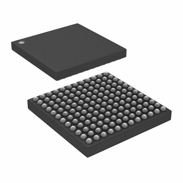
128Mb AS4C4M32D1A - 144 ball FBGA PACKAGE
Revision
Rev 1.0
Details
Preliminary datasheet
Date
May. 2016
Alliance Memory Inc. 511 Taylor Way, San Carlos, CA 94070 TEL: (650) 610-6800 FAX: (650) 620-9211
Alliance Memory Inc. reserves the right to change products or specification without notice
Confidential
- 1/64 -
Rev.1.0 May 2016
�AS4C4M32D1A-5BIN
AS4C4M32D1A-5BCN
Features
Overview
• Fast clock rate: 200 MHz
The 128Mb DDR SDRAM is a high-speed CMOS
double data rate synchronous DRAM containing 128
Mbits. It is internally configured as a quad 1M x 32
DRAM with a synchronous interface (all signals are
registered on the positive edge of the clock signal, CK).
Data outputs occur at both rising edges of CK and CK .
Read and write accesses to the SDRAM are burst
oriented; accesses start at a selected location and
continue for a programmed number of locations in a
programmed sequence. Accesses begin with the
registration of a BankActivate command, which is then
followed by a Read or Write command. The device
provides programmable Read or Write burst lengths of
2, 4, 8. An auto precharge function may be enabled to
provide a self-timed row precharge that is initiated at the
end of the burst sequence. The refresh functions, either
Auto or Self Refresh are easy to use. In addition, 128Mb
DDR SDRAM features programmable DLL option. By
having a programmable mode register and extended
mode register, the system can choose the most suitable
modes to maximize its performance. These devices are
well suited for applications requiring high memory
bandwidth; result in a device particularly well suited to
high performance main memory and graphics
applications.
• Differential Clock CK & CK input
• 4 Bi-directional DQS. Data transactions on both
edges of DQS (1DQS / Byte)
• DLL aligns DQ and DQS transitions
• Edge aligned data & DQS output
• Center aligned data & DQS inpu
• 4 internal banks, 1M x 32-bit for each bank
• Programmable mode and extended mode registers
- CAS Latency: 2, 2.5, 3
- Burst length: 2, 4, 8
- Burst Type: Sequential & Interleave
• All inputs except DQ’s & DM are at the positive
edge of the system clock
• 4 individual DM control for write masking only
• Auto Refresh and Self Refresh
• 4096 refresh cycles / 64ms
• Operating Temperature:
- Industrial -40°C~85°C
- Commercial 0°C to 70°C
Power
supplies: VDD & VDDQ = 2.5V ± 0.2V
•
• Interface: SSTL_2 I/O compatible
• 144-ball 12 x 12 x 1.4mm LFBGA package
-Pb and Halogen Free
Table 1. Ordering Information
Part Number
Org
Temperature
MaxClock (MHz)
Package
AS4C4M32D1A-5BCN
4Mx32
Commercial 0°C to 70°C
200
144-ball FBGA
AS4C4M32D1A-5BIN
4Mx32
Industrial -40°C to 85°C
200
144-ball FBGA
Table 2. Speed Grade Information
Speed Grade
Clock Frequency
CAS Latency
tRCD (ns)
DDR1-400
Confidential
3
200MHz
- 2/64 -
15
tRP (ns)
15
Rev.1.0 May 2016
�AS4C4M32D1A-5BIN
AS4C4M32D1A-5BCN
Figure 1. Pin Assignment (LFBGA 144Ball Top View)
4
5
6
7
8
1
2
3
9
10
11
12
A
DQS0
DM0
VSSQ
DQ3
DQ2
DQ0
DQ31
DQ29
DQ28
VSSQ
DM3
DQS3
B
DQ4
VDDQ
NC
VDDQ
DQ1
VDDQ
VDDQ
DQ30
VDDQ
NC
VDDQ
DQ27
C
DQ6
DQ5
VSSQ
VSSQ
VSSQ
VDD
VDD
VSSQ
VSSQ
VSSQ
DQ26
DQ25
D
DQ7
VDDQ
VDD
VSS
VSSQ
VSS
VSS
VSSQ
VSS
VDD
VDDQ
DQ24
E
DQ17
DQ16
VDDQ
VSSQ
VSS
VSS
VSS
VSS
VSSQ
VDDQ
DQ15
DQ14
F
DQ19
DQ18
VDDQ
VSSQ
VSS
VSS
VSS
VSS
VSSQ
VDDQ
DQ13
DQ12
G
DQS2
DM2
NC
VSSQ
VSS
VSS
VSS
VSS
VSSQ
NC
DM1
DQS1
H
DQ21
DQ20
VDDQ
VSSQ
VSS
VSS
VSS
VSS
VSSQ
VDDQ
DQ11
DQ10
J
DQ22
DQ23
VDDQ
VSSQ
VSS
VSS
VSS
VSS
VSSQ
VDDQ
DQ9
DQ8
K
CAS
WE
VDD
VSS
A10
VDD
VDD
NC
VSS
VDD
NC
NC
L
RAS
NC
NC
BA1
A2
A11
A9
A5
NC
CK
CK
NC
M
CS
NC
BA0
A0
A1
A3
A4
A6
A7
A8
CKE
VREF
Confidential
- 3/64 -
Rev.1.0 May 2016
�AS4C4M32D1A-5BIN
AS4C4M32D1A-5BCN
Table 3. Pin Assignment by Name (LFBGA 144Ball)
Symbol Location Symbol Location Symbol Location Symbol Location Symbol Location Symbol Location Symbol Location Symbol
A0
M4
DQ6
C1
DQ24 D12
CK
L10 VDDQ B6
VSS
E5
VSS
J7
VSSQ
A1
M5
DQ7
D1
DQ25 C12
L11 VDDQ B7
VSS
E6
VSS
J8
VSSQ
CK
A2
L5
DQ8
J12 DQ26 C11
CKE M11 VDDQ B9
VSS
E7
VSS
K4 VSSQ
A3
M6
DQ9
J11 DQ27 B12
M1 VDDQ B11
VSS
E8
VSS
K9 VSSQ
CS
A4
M7
DQ10
H12
DQ28
A9
A5
L8
DQ11
H11
DQ29
A8
RAS
CAS
A6
A7
A8/AP
A9
A10
A11
DQ0
DQ1
DQ2
DQ3
DQ4
DQ5
M8
M9
M10
L7
K5
L6
A6
B5
A5
A4
B1
C2
DQ12
DQ13
DQ14
DQ15
DQ16
DQ17
DQ18
DQ19
DQ20
DQ21
DQ22
DQ23
F12
F11
E12
E11
E2
E1
F2
F1
H2
H1
J1
J2
DQ30
DQ31
DQS0
DQS1
DQS2
DQS3
DM0
DM1
DM2
DM3
BA0
BA1
B8
A7
A1
G12
G1
A12
A2
G11
G2
A11
M3
L4
VREF
VDD
VDD
VDD
VDD
VDD
VDD
VDD
VDD
VDDQ
VDDQ
Confidential
WE
Location
G4
G9
H4
H9
L1
VDDQ
D2
VSS
F5
VSSQ
A3
VSSQ
J4
K1
VDDQ
D11
VSS
F6
VSSQ
A10
VSSQ
J9
K2
M12
C6
C7
D3
D10
K3
K6
K7
K10
B2
B4
VDDQ
VDDQ
VDDQ
VDDQ
VDDQ
VDDQ
VDDQ
VDDQ
VSS
VSS
VSS
VSS
E3
E10
F3
F10
H3
H10
J3
J10
D4
D6
D7
D9
VSS
VSS
VSS
VSS
VSS
VSS
VSS
VSS
VSS
VSS
VSS
VSS
F7
F8
G5
G6
G7
G8
H5
H6
H7
H8
J5
J6
VSSQ
VSSQ
VSSQ
VSSQ
VSSQ
VSSQ
VSSQ
VSSQ
VSSQ
VSSQ
VSSQ
VSSQ
C3
C4
C5
C8
C9
C10
D5
D8
E4
E9
F4
F9
NC
NC
NC
NC
NC
NC
NC
NC
NC
NC
NC
NC
B3
B10
G3
G10
K8
K11
K12
L2
L3
L9
L12
M2
- 4/64 -
Rev.1.0 May 2016
�AS4C4M32D1A-5BIN
AS4C4M32D1A-5BCN
Figure 2. Block Diagram
DLL
CLOCK
BUFFER
Row
Decoder
CKE
COMMAND
DECODER
A8/AP
COLUMN
COUNTER
DQS0~3
DQ0
MODE
REGISTER
ADDRESS
BUFFER
REFRESH
COUNTER
DATA
STROBE
BUFFER
4096 x 256 x 32
CELL ARRAY
(BANK #2)
Column Decoder
DQ
Buffer
~
DQ31
DM0~3
Confidential
4096 x 256 x 32
CELL ARRAY
(BANK #1)
Column Decoder
Row
Decoder
A9
A10
A11
BA0
BA1
CONTROL
SIGNAL
GENERATOR
Row
Decoder
~
A0
4096 x 256 x 32
CELL ARRAY
(BANK #0)
Column Decoder
CS
RAS
CAS
WE
Row
Decoder
CK
CK
- 5/64 -
4096 x 256 x 32
CELL ARRAY
(BANK #3)
Column Decoder
Rev.1.0 May 2016
�AS4C4M32D1A-5BIN
AS4C4M32D1A-5BCN
Pin Descriptions
Symbol
CK, CK
Type
Input
CKE
Input
BA0, BA1
Input
A0-A11
Input
CS
Input
RAS
Input
Table 4. Pin Details
Description
Differential Clock: CK, CK are driven by the system clock. All SDRAM input
commands are sampled on the positive edge of CK. Both CK and CK increment the
internal burst counter and controls the output registers.
Clock Enable: CKE activates (HIGH) and deactivates (LOW) the CK signal. If CKE
goes low synchronously with clock, the internal clock is suspended from the next
clock cycle and the state of output and burst address is frozen as long as the CKE
remains low. When all banks are in the idle state, deactivating the clock controls the
entry to the Power Down and Self Refresh modes.
Bank Activate: BA0 and BA1 define to which bank the BankActivate, Read, Write, or
BankPrecharge command is being applied. They also define which Mode Register or
Extended Mode Register is loaded during a Mode Register Set command.
Address Inputs: A0-A11 are sampled during the Bank Activate command (row
address A0-A11) and Read/Write command (column address A0-A7 with A8 defining
Auto Precharge) to select one location out of the 1M available in the respective bank.
During a Precharge command, A8 is sampled to determine if all banks are to be
precharged (A8 = HIGH). The address inputs also provide the op-code during a Mode
Register Set or Extended Mode Register Set command.
Chip Select: CS enables (sampled LOW) and disables (sampled HIGH) the
command decoder. All commands are masked when CS is sampled HIGH. CS
provides for external bank selection on systems with multiple banks. It is considered
part of the command code.
Row Address Strobe: The RAS signal defines the operation commands in
conjunction with the CAS and /WE signals and is latched at the positive edges of CK.
When RAS and CS are asserted "LOW" and CAS is asserted "HIGH" either the
BankActivate command or the Precharge command is selected by the WE signal.
When the WE is asserted "HIGH," the BankActivate command is selected and the
bank designated by BA is turned on to the active state. When the WE is asserted
"LOW," the Precharge command is selected and the bank designated by BA is
switched to the idle state after the precharge operation.
CAS
Input
Column Address Strobe: The CAS signal defines the operation commands in
conjunction with the RAS and /WE signals and is latched at the positive edges of CK.
When /RAS is held "HIGH" and CS is asserted "LOW" the column access is started
by asserting CAS "LOW" Then, the Read or Write command is selected by asserting
WE "HIGH " or “LOW".
WE
Input
DQS0-DQS3
Input /
Output
DM0 - DM3
Input
DQ0 - DQ31
VDD
VSS
Input /
Output
Supply
Supply
VDDQ
Supply
Confidential
Write Enable: The WE signal defines the operation commands in conjunction with
the RAS and CAS signals and is latched at the positive edges of CK. The WE input
is used to select the BankActivate or Precharge command and Read or Write
command.
Bidirectional Data Strobe: The DQSx signals are mapped to the following data
bytes: DQS0 to DQ0-DQ7, DQS1 to DQ8-DQ15, DQS2 to DQ16-DQ23, and DQS3 to
DQ24-DQ31.
Data Input Mask: DM0-DM3 are byte specific. Input data is masked when DM is
sampled HIGH during a write cycle. DM3 masks DQ31-DQ24, DM2 masks DQ23DQ16, DM1 masks DQ15-DQ8, and DM0 masks DQ7-DQ0.
Data I/O: The DQ0-DQ31 input and output data are synchronized with positive and
negative edges of DQS0~DQS3. The I/Os are byte-maskable during Writes.
Power Supply: Power for the input buffers and core logic.
Ground: Ground for the input buffers and core logic.
DQ Power: Provide isolated power to DQs for improved noise immunity.
- 6/64 -
Rev.1.0 May 2016
�AS4C4M32D1A-5BIN
AS4C4M32D1A-5BCN
VSSQ
VREF
NC
Confidential
Supply
Supply
-
DQ Ground: Provide isolated ground to DQs for improved noise immunity.
Reference Voltage for Inputs: +0.5 x VDDQ
No Connect: No internal connection, these pins suggest to be left unconnected.
- 7/64 -
Rev.1.0 May 2016
�AS4C4M32D1A-5BIN
AS4C4M32D1A-5BCN
Operation Mode
Table 5 shows the truth table for the operation commands.
Table 5. Truth Table (Note (1), (2))
Command
State
BankActivate
BankPrecharge
Precharge All
Write
Write and AutoPrecharge
Read
Read and Autoprecharge
Mode Register Set
Extended Mode Register Set
No-Operation
Device Deselect
Burst Stop
AutoRefresh
SelfRefresh Entry
Idle(3)
SelfRefresh Exit
Power Down Mode Entry
Any
Any
Active(3)
Active(3)
Active(3)
Active(3)
Idle
Idle
Any
Any
Active(4)
Idle
Idle
Idle
(Self Refresh)
Idle/Active(5)
CKEn-1 CKEn DM BA1 BA0
A8 A11-A9, A7-0 CS
H
H
H
H
H
H
H
H
H
H
H
H
H
H
X
X
X
X
X
X
X
X
X
X
X
X
H
L
X
X
X
V
V
X
X
X
X
X
X
X
X
X
V
V
X
V
V
V
V
L
L
X
X
X
X
X
V
V
X
V
V
V
V
L
H
X
X
X
X
X
Row Address
L
X
H
X
L
Column
H
Address
L
A0~A7
H
X
X
X
X
X
X
X
X
X
X
L
H
X
X
X
X
X
H
L
X
X
X
X
X
OP code
L
L
L
L
L
L
L
L
L
L
H
L
L
L
H
L
H
L
H
L
X
X
RAS CAS
L
L
L
H
H
H
H
L
L
H
X
H
L
L
X
H
X
H
X
H
X
X
Any
L
H X X
X
X
X
(Power Down)
Data Mask Enable(6)
Active
H
X H X
X
X
X
Data Mask Disable
Active
H
X
L X
X
X
X
Note: 1. V = Valid data, X = Don't Care, L = Low level, H = High level
2. CKEn signal is input level when commands are provided.
CKEn-1 signal is input level one clock cycle before the commands are provided.
3. These are states of bank designated by BA0, BA1signals.
4. Read burst stop with BST command for all burst types.
5. Power Down Mode can not enter in the burst operation.
When this command is asserted in the burst cycle, device state is clock suspend mode.
6. DM0 – DM3 can be enabled respectively.
Power Down Mode Exit
Confidential
- 8/64 -
H
H
H
L
L
L
L
L
L
H
X
H
L
L
X
H
X
H
X
H
X
X
WE
H
L
L
L
L
H
H
L
L
H
X
L
H
H
X
H
X
H
X
H
X
X
Rev.1.0 May 2016
�AS4C4M32D1A-5BIN
AS4C4M32D1A-5BCN
Mode Register Set (MRS)
The Mode Register stores the data for controlling various operating modes of a DDR SDRAM. It programs
CAS Latency, Burst Type, and Burst Length to make the DDR SDRAM useful for a variety of applications. The
default value of the Mode Register is not defined; therefore the Mode Register must be written by the user.
Values stored in the register will be retained until the register is reprogrammed. The Mode Register is written by
asserting Low on CS , RAS , CAS , WE , BA1 and BA0 (the device should have all banks idle with no bursts in
progress prior to writing into the mode register, and CKE should be High). The state of address pins A0~A11 and
BA0, BA1 in the same cycle in which CS , RAS , CAS and WE are asserted Low is written into the Mode
Register. A minimum of two clock cycles, tMRD, are required to complete the write operation in the Mode
Register. The Mode Register is divided into various fields depending on functionality. The Burst Length uses
A0~A2, Burst Type uses A3, and CAS Latency (read latency from column address) uses A4~A6. A logic 0 should
be programmed to all the undefined addresses to ensure future compatibility. Reserved states should not be
used to avoid unknown device operation or incompatibility with future versions. Refer to the table for specific
codes for various burst lengths, burst types and CAS latencies.
Table 6. Mode Register Bitmap
BA1 BA0 A11
0
A8
0
1
X
0
A10
A9
A8
0
A7
Test Mode
0 Normal mode
0
DLL Reset
1
Test mode
BA0 Mode
0
MRS
1 EMRS
A7
T.M.
A6
A5
CAS Latency
A6 A5 A4 CAS Latency
Reserved
0 0 0
Reserved
0 0 1
0
0
1
1
1
1
1
1
0
0
1
1
0
1
0
1
0
1
A4
A3
BT
A2
A1
A0
Burst Length
A3 Burst Type
0 Sequential
A2 A1 A0
0 0 0
Address Field
Mode Register
Burst Length
Reserved
0
0
1
2
2
0
1
0
4
3
Reserved
Reserved
2.5
Reserved
0
1
1
1
1
1
0
0
1
1
1
0
1
0
1
8
Reserved
Reserved
Reserved
Reserved
1
Interleave
• Burst Length Field (A2~A0)
This field specifies the data length of column access using the A2~A0 pins and selects the Burst Length to be
2, 4, and 8.
Table 7. Burst Length
A2
A1
A0
Burst Length
0
0
0
Reserved
0
0
1
2
0
1
0
4
0
1
1
8
1
0
0
Reserved
1
0
1
Reserved
1
1
0
Reserved
1
1
1
Reserved
Confidential
- 9/64 -
Rev.1.0 May 2016
�AS4C4M32D1A-5BIN
AS4C4M32D1A-5BCN
• Addressing Mode Select Field (A3)
The Addressing Mode can be one of two modes, either Interleave Mode or Sequential Mode. Both Sequential
Mode and Interleave Mode support burst length of 2, 4, and 8.
Table 8. Addressing Mode
•
A3
Addressing Mode
0
Sequential
1
Interleave
Burst Definition, Addressing Sequence of Sequential and Interleave Mode
Table 9. Burst Address ordering
Burst
Length
2
4
8
Start Address
A2
A1
A0
X
X
0
X
X
1
X
0
0
X
0
1
X
1
0
X
1
1
0
0
0
0
0
1
0
1
0
0
1
1
1
0
0
1
0
1
1
1
0
1
1
1
Sequential
Interleave
0, 1
1, 0
0, 1, 2, 3
1, 2, 3, 0
2, 3, 0, 1
3, 0, 1, 2
0, 1, 2, 3, 4, 5, 6, 7
1, 2, 3, 4, 5, 6, 7, 0
2, 3, 4, 5, 6, 7, 0, 1
3, 4, 5, 6, 7, 0, 1, 2
4, 5, 6, 7, 0, 1, 2, 3
5, 6, 7, 0, 1, 2, 3, 4
6, 7, 0, 1, 2, 3, 4, 5
7, 0, 1, 2, 3, 4, 5, 6
0, 1
1, 0
0, 1, 2, 3
1, 0, 3, 2
2, 3, 0, 1
3, 2, 1, 0
0, 1, 2, 3, 4, 5, 6, 7
1, 0, 3, 2, 5, 4, 7, 6
2, 3, 0, 1, 6, 7, 4, 5
3, 2, 1, 0, 7, 6, 5, 4
4, 5, 6, 7, 0, 1, 2, 3
5, 4, 7, 6, 1, 0, 3, 2
6, 7, 4, 5, 2, 3, 0, 1
7, 6, 5, 4, 3, 2, 1, 0
• CAS Latency Field (A6~A4)
This field specifies the number of clock cycles from the assertion of the Read command to the first read data.
The minimum whole value of CAS Latency depends on the frequency of CK. The minimum whole value
satisfying the following formula must be programmed into this field. tCAC (min) ≤ CAS Latency X tCK
Table 10. CAS Latency
Confidential
A6
A5
A4
CAS Latency
0
0
0
Reserved
0
0
1
Reserved
0
1
0
2 clocks
0
1
1
3 clocks
1
0
0
Reserved
1
0
1
Reserved
1
1
0
2.5 clocks
1
1
1
Reserved
- 10/64 -
Rev.1.0 May 2016
�AS4C4M32D1A-5BIN
AS4C4M32D1A-5BCN
• Test Mode Field (A8~A7)
These two bits are used to enter the test mode and must be programmed to "00" in normal operation.
Table 11. Test Mode
•
A8
A7
Test Mode
0
0
Normal mode
1
0
DLL Reset
X
1
Test mode
(BA0, BA1)
Table 12. MRS/EMRS
BA1
BA0
A11 ~ A0
RFU
0
MRS Cycle
RFU
1
Extended Functions (EMRS)
Extended Mode Register Set (EMRS)
The Extended Mode Register Set stores the data for enabling or disabling DLL and selecting output driver
strength. The default value of the extended mode register is not defined, therefore must be written after power up
for proper operation. The extended mode register is written by asserting low on CS , RAS , CAS , and WE . (the
device should have all banks idle with no bursts in progress prior to writing into the mode register, and CKE
should be High)The state of A0 ~ A11 and BA1 are written in the mode register in the same cycle
as CK , RAS , CAS , and WE going low. The DDR SDRAM should be in all bank precharge with CKE already high
prior to writing into the extended mode register. A1 is used for setting driver strength. Two clock cycles are
required to complete the write operation in the extended mode register. The mode register contents can be
changed using the same command and clock cycle requirements during operation as long as all banks are in the
idle state. A0 is used for DLL enable or disable. "High" on BA0 is used for EMRS. Refer to the table for specific
codes.
Table 13. Extended Mode Register Bitmap
BA1 BA0 A11
0
1
A10
A9
A8
A7
A6
A5
A4
A3
A2
RFU must be set to “0”
A1
DS
A0
DLL Extended Mode Register
BA0
0
Mode
MRS
A1
0
Drive Strength
Full
A0
0
Enable
1
EMRS
1
Reserved
1
Disable
Confidential
- 11/64 -
Address Field
DLL
Rev.1.0 May 2016
�AS4C4M32D1A-5BIN
AS4C4M32D1A-5BCN
Table 14. Absolute Maximum Rating
VIN, VOUT
Input, Output Voltage
Rating
-5
- 0.5 ~ VDDQ+0.5
VDD, VDDQ
Power Supply Voltage
-1 ~ 3.6
V
1,2
0~70
°C
°C
1
°C
°C
W
1
Symbol
TA
TSTG
TSOLDER
PD
Item
Ambient Temperature Commercial
Industrial
-40~85
- 55~150
Storage Temperature
Soldering Temperature (10s)
260
Power Dissipation
2.0
Unit
Note
V
1,2
1
1
1
IOS
50
mA
1
Short Circuit Output Current
Note1: Stress greater than those listed under “Absolute Maximum Ratings” may cause permanent damage of the
devices
Note2: These voltages are relative to Vss
Table 15. Recommended D.C. Operating Conditions (SSTL_2 In/Out, TA = -40 ~ 85 °C)
Symbol
VDD
Parameter
Power Supply Voltage
Min.
2.3
Max.
2.7
Unit
V
Note
1
2.3
2.7
V
1
VDDQ
Power Supply Voltage(for I/O )
VREF
Input Reference Voltage
0.49 x VDDQ
0.51 x VDDQ
V
VTT
Termination Voltage
VREF – 0.04
VREF + 0.04
V
Input High Voltage
VREF + 0.15
VDDQ + 0.3
V
Input Low Voltage
VSSQ - 0.3
VREF- 0.15
V
VIH(DC)
VIL(DC)
IIL
Input Leakage Current
-2
2
µA
IOZ
Output Leakage Current
-5
5
µA
IOH
Output High Current
-16.2
-
mA
VOH = 1.95V
IOL
Output Low Current
16.2
-
mA
VOL = 0.35V
Min.
Max.
Unit
Table 16. Capacitance (VDD = 2.5V, f = 1MHz, TA = 25 °C)
Symbol
Parameter
CIN1
Input Capacitance (CK, CK )
1.5
2.5
pF
CIN2
Input Capacitance (All other input-only pins)
1.5
2.5
pF
CI/O
DM, DQ, DQS Input/Output Capacitance
3.5
4.5
pF
Note: These parameters are guaranteed by design, periodically sampled and are not 100% tested.
Table 17. Decoupling Capacitance Guide Line
Symbol
Parameter
CDC1 Decouping Capacitance between VDD and VSS
CDC2
Confidential
Decouping Capacitance between VDDQ and VSSQ
- 12/64 -
Value
0.1+0.01
0.1+0.01
Unit
µF
µF
Rev.1.0 May 2016
�AS4C4M32D1A-5BIN
AS4C4M32D1A-5BCN
Table 18. D.C. Characteristics (VDD=2.5V ± 0.2V, TA =-40~85°C)
Parameter & Test Condition
OPERATING CURRENT: One bank; Active-Precharge; tRC=tRC (min);
tCK=tCK (min); DQ, DM and DQS inputs changing once per clock cycle;
Address and control inputs changing once every two clock cycles.
OPERATING CURRENT : One bank; Active-Read-Precharge; BL=4;
tRC=tRC(min); tCK=tCK(min); lout=0mA; Address and control inputs
changing once per clock cycle
PRECHARGE POWER-DOWN STANDBY CURRENT: All banks idle;
power-down mode; tCK=tCK(min); CKE=LOW
IDLE STANDBY CURRENT : CKE = HIGH; CS =HIGH(DESELECT); All
banks idle; tCK=tCK(min); Address and control inputs changing once per
clock cycle; VIN=VREF for DQ, DQS and DM
ACTIVE POWER-DOWN STANDBY CURRENT : one bank active; powerdown mode; CKE=LOW; tCK=tCK(min)
Symbol
-5
Max.
Unit
IDD0
210
mA
IDD1
240
mA
IDD2P
75
mA
IDD2N
100
mA
IDD3P
75
mA
220
mA
420
mA
420
mA
300
mA
6
mA
570
mA
ACTIVE STANDBY CURRENT : CS =HIGH;CKE=HIGH; one bank active ;
IDD3N
tRC=tRC(max);tCK=tCK(min);Address and control inputs changing once per
clock cycle; DQ,DQS,and DM inputs changing twice per clock cycle
OPERATING CURRENT BURST READ : BL=2; READs; Continuous burst;
one bank active; Address and control inputs changing once per clock cycle; IDD4R
tCK=tCK(min); lout=0mA;50% of data changing on every transfer
OPERATING CURRENT BURST Write : BL=2; WRITES; Continuous
Burst ;one bank active; address and control inputs changing once per clock
IDD4W
cycle; tCK=tCK(min); DQ,DQS,and DM changing twice per clock cycle; 50%
of data changing on every transfer
AUTO REFRESH CURRENT :
IDD5
tRC=tRFC(min); tCK=tCK(min)
SELF REFRESH CURRENT:
IDD6
Self Refresh Mode ; CKE≦0.2V;tCK=tCK(min)
BURST OPERATING CURRENT 4 bank operation:
Four bank interleaving READs; BL=4;with Auto Precharge; tRC=tRC(min);
tCK=tCK(min); Address and control inputs change only during Active,
READ , or WRITE command
IDD7
Note:
1. Stress greater than those listed under "Absolute Maximum Ratings" may cause permanent damage of the
device.
2. All voltages are referenced to VSS.
3. These parameters depend on the cycle rate and these values are measured by the cycle rate under the
minimum value of tCK and tRC. Input signals are changed one time during tCK.
4. Power-up sequence is described in later page.
Confidential
- 13/64 -
Rev.1.0 May 2016
�AS4C4M32D1A-5BIN
AS4C4M32D1A-5BCN
Table 19. Electrical Characteristics and Recommended A.C. Operating Conditions
(VDD = 2.5V ± 0.2V, TA = -40~85 °C)
Symbol
-5
Parameter
tCK
Clock cycle time
tCH
tCL
Clock high level width
Clock low level width
tDQSCK
DQS-out access time from CK, CK
-0.6
0.6
ns
tAC
-0.7
0.7
ns
tDQSQ
tRPRE
tRPST
tDQSS
tWPRES
tWPRE
tWPST
tDQSH
tDQSL
tIS
tIH
tDS
tDH
tHP
tQH
tRC
tRFC
tRAS
tRCD
tRP
tRRD
tWR
tMRD
tDAL
tXSRD
tPDEX
tREFI
tIPW
tDIPW
Output access time from CK, CK
DQS-DQ Skew
Read preamble
Read postamble
CK to valid DQS-in
DQS-in setup time
DQS Write preamble
DQS write postamble
DQS in high level pulse width
DQS in low level pulse width
Address and Control input setup time
Address and Control input hold time
DQ & DM setup time to DQS
DQ & DM hold time to DQS
Clock half period
DQ/DQS output hold time from DQS
Row cycle time
Refresh row cycle time
Row active time
Active to Read or Write delay
Row precharge time
Row active to Row active delay
Write recovery time
Mode register set cycle time
Auto precharge write recovery + Precharge time
Self refresh exit to read command delay
Power down exit time
Average Refresh interval time
Control and Address input pulse width
DQ & DM input pulse width (for each input)
0.9
0.4
0.72
0
0.25
0.4
0.4
0.4
0.7
0.7
0.4
0.4
tCLMIN or tCHMIN
tHP - tQHS
55
70
40
15
15
2
3
2
tWR + tRP
200
tCK + tIS
2.2
1.75
0.4
1.1
0.6
1.25
0.6
100K
15.6
-
ns
tCK
tCK
tCK
ns
tCK
tCK
tCK
tCK
ns
ns
ns
ns
ns
ns
ns
ns
ns
ns
ns
tCK
tCK
tCK
tCK
tCK
ns
µs
ns
ns
tHZ
Data-out high-impedance window from CK/ CK
-
0.7
ns
tLZ
Data-out low-impedance window from CK/ CK
-0.7
0.7
ns
tQHS
Data Hold Skew Factor
Output data valid window
Exit Self-Refresh to non-Read command
CAS# to CAS# Delay time
DQS falling edge to CK setup time
DQS falling edge hold time from CK
tQH - tDQSQ
75
1
0.2
0.2
0.5
-
ns
ns
ns
tCK
tCK
tCK
DVW
tXSNR
tCCD
tDSS
tDSH
Confidential
CL = 2
CL = 2.5
CL = 3
- 14/64 -
Max.
12
12
7.5
0.55
0.55
Unit
Min.
7.5
6
5
0.45
0.45
ns
ns
ns
tCK
tCK
Rev.1.0 May 2016
�AS4C4M32D1A-5BIN
AS4C4M32D1A-5BCN
Table 20. Recommended A.C. Operating Conditions (TA = -40~85 °C, VDD=2.5V ± 0.2V)
Parameter
-5
Symbol
Min.
Max.
Unit
Input High Voltage (AC)
VIH (AC)
VREF + 0.31
-
V
Input Low Voltage (AC)
VIL (AC)
-
VREF – 0.31
V
Input Different Voltage, CK and CK inputs
VID (AC)
0.7
VDDQ + 0.6
V
0.5*VDDQ-0.2
0.5*VDDQ+0.2
V
Input Crossing Point Voltage, CK and CK inputs VIX (AC)
Note:
1. All voltages are referenced to VSS.
2. These parameters depend on the cycle rate and these values are measured by the cycle rate under the
minimum value of tCK and tRC. Input signals are changed one time during tCK.
3. Power-up sequence is described in Note 5.
4. A.C. Test Conditions
Table 21. SSTL_2 Interface
Reference Level of Output Signals (VREF)
0.5 * VDDQ
Output Load
Reference to the Test Load
Input Signal Levels
VREF+0.31 V / VREF-0.31 V
Input Signals Slew Rate
1 V/ns
Reference Level of Input Signals
0.5 * VDDQ
Figure 3. SSTL_2 A.C. Test Load
0.5 * VDDQ
50Ω
DQ, DQS
Z0=50Ω
Confidential
- 15/64 -
30pF
Rev.1.0 May 2016
�AS4C4M32D1A-5BIN
AS4C4M32D1A-5BCN
5. Power up Sequence
Power up must be performed in the following sequence.
1) Apply power to VDD before or at the same time as VDDQ, VTT and VREF when all input signals are held
"NOP" state and maintain CKE “LOW”.
2) Start clock and maintain stable condition for minimum 200us.
3) Issue a “NOP” command and keep CKE “HIGH”
4) Issue a “Precharge All” command.
5) Issue EMRS – enable DLL.
6) Issue MRS – reset DLL. (An additional 200 clock cycles are required to lock the DLL).
7) Precharge all banks of the device.
8) Issue two or more Auto Refresh commands.
9) Issue MRS – with A8 to low to initialize the mode register.
Confidential
- 16/64 -
Rev.1.0 May 2016
�AS4C4M32D1A-5BIN
AS4C4M32D1A-5BCN
Timing Waveforms
Figure 4. Activating a Specific Row in a Specific Bank
CK
CK
CKE
HIGH
CS
RAS
CAS
WE
Address
RA
BA0,1
BA
RA=Row Address
BA=Bank Address
Don’t Care
Confidential
- 17/64 -
Rev.1.0 May 2016
�AS4C4M32D1A-5BIN
AS4C4M32D1A-5BCN
Figure 5. tRCD and tRRD Definition
CK
CK
COMMAND
ACT
Address
Row
Row
Col
BA0,BA1
Bank A
Bank B
Bank B
NOP
NOP
ACT
tRRD
NOP
NOP
RD/WR
NOP
tRCD
Don’t Care
Figure 6. READ Command
CK
CK
CKE
HIGH
CS
RAS
CAS
WE
A0 ~ A7
CA
EN AP
A8
DIS AP
BA0,1
BA
CA=Column Address
BA=Bank Address
EN AP=Enable Autoprecharge
DIS AP=Disable Autoprecharge
Don’t Care
Confidential
- 18/64 -
Rev.1.0 May 2016
�AS4C4M32D1A-5BIN
AS4C4M32D1A-5BCN
Figure 7. Read Burst Required CAS Latencies (CL=2)
CK
CK
COMMAND
READ
ADDRESS
Bank A,
Col n
NOP
NOP
NOP
NOP
NOP
CL=2
DQS
DO
n
DQ
DO n=Data Out from column n
Burst Length=4
3 subsequent elements of Data Out appear in the programmed order
following DO n
Don’t Care
Read Burst Required CAS Latencies (CL=2.5)
CK
CK
COMMAND
READ
ADDRESS
Bank A,
Col n
NOP
NOP
NOP
NOP
NOP
CL=2.5
DQS
DO
n
DQ
DO n=Data Out from column n
Burst Length=4
3 subsequent elements of Data Out appear in the programmed order following DO n
Don’t Care
Confidential
- 19/64 -
Rev.1.0 May 2016
�AS4C4M32D1A-5BIN
AS4C4M32D1A-5BCN
Read Burst Required CAS Latencies (CL=3)
CK
CK
COMMAND
READ
ADDRESS
Bank A,
Col n
NOP
NOP
NOP
NOP
NOP
CL=3
DQS
DO
n
DQ
DO n=Data Out from column n
Burst Length=4
3 subsequent elements of Data Out appear in the programmed order
following DO n
Don’t Care
Confidential
- 20/64 -
Rev.1.0 May 2016
�AS4C4M32D1A-5BIN
AS4C4M32D1A-5BCN
Figure 8. Consecutive Read Bursts Required CAS Latencies (CL=2)
CK
CK
COMMAND
ADDRESS
READ
NOP
READ
NOP
NOP
NOP
Bank,
Col o
Bank,
Col n
CL=2
DQS
DQ
DO
n
DO
o
DO n (or o)=Data Out from column n (or column o)
Burst Length=4 or 8 (if 4, the bursts are concatenated; if 8, the second burst interrupts the first)
3 subsequent elements of Data Out appear in the programmed order following DO n
3 (or 7) subsequent elements of Data Out appear in the programmed order following DO o
Read commands shown must be to the same device
Don’t Care
Confidential
- 21/64 -
Rev.1.0 May 2016
�AS4C4M32D1A-5BIN
AS4C4M32D1A-5BCN
Consecutive Read Bursts Required CAS Latencies (CL=2.5)
CK
CK
COMMAND
ADDRESS
READ
NOP
READ
NOP
NOP
NOP
Bank,
Col o
Bank,
Col n
CL=2.5
DQS
DO
n
DQ
DO
o
DO n (or o)=Data Out from column n (or column o)
Burst Length=4 or 8 (if 4, the bursts are concatenated; if 8, the second burst interrupts the first)
3 subsequent elements of Data Out appear in the programmed order following DO n
3 (or 7) subsequent elements of Data Out appear in the programmed order following DO o
Read commands shown must be to the same device
Don’t Care
Confidential
- 22/64 -
Rev.1.0 May 2016
�AS4C4M32D1A-5BIN
AS4C4M32D1A-5BCN
Consecutive Read Bursts Required CAS Latencies (CL=3)
CK
CK
COMMAND
ADDRESS
READ
NOP
Bank,
Col n
READ
NOP
NOP
NOP
Bank,
Col o
CL=3
DQS
DO
n
DQ
DO
o
DO n (or o)=Data Out from column n (or column o)
Burst Length=4 or 8 (if 4, the bursts are concatenated; if 8, the second burst interrupts the first)
3 subsequent elements of Data Out appear in the programmed order following DO n
3 (or 7) subsequent elements of Data Out appear in the programmed order following DO o
Read commands shown must be to the same device
Don’t Care
Confidential
- 23/64 -
Rev.1.0 May 2016
�AS4C4M32D1A-5BIN
AS4C4M32D1A-5BCN
Figure 9. Non-Consecutive Read Bursts Required CAS Latencies (CL=2)
CK
CK
COMMAND
ADDRESS
READ
NOP
NOP
READ
NOP
NOP
Bank,
Col o
Bank,
Col n
CL=2
DQS
DO
n
DQ
DO
o
DO n (or o)=Data Out from column n (or column o)
Burst Length=4
3 subsequent elements of Data Out appear in the programmed order following DO n
(and following DO o)
Don’t Care
Non-Consecutive Read Bursts Required CAS Latencies (CL=2.5)
CK
CK
COMMAND
ADDRESS
READ
NOP
NOP
READ
NOP
NOP
NOP
Bank,
Col o
Bank,
Col n
CL=2.5
DQS
DQ
DO
n
DO
o
DO n (or o)=Data Out from column n (or column o)
Burst Length=4
3 subsequent elements of Data Out appear in the programmed order following DO n
(and following DO o)
Don’t Care
Confidential
- 24/64 -
Rev.1.0 May 2016
�AS4C4M32D1A-5BIN
AS4C4M32D1A-5BCN
Non-Consecutive Read Bursts Required CAS Latencies (CL=3)
CK
CK
COMMAND
ADDRESS
READ
NOP
NOP
READ
NOP
NOP
NOP
Bank,
Col o
Bank,
Col n
CL=3
DQS
DO
n
DQ
DO
o
DO n (or o)=Data Out from column n (or column o)
Burst Length=4
3 subsequent elements of Data Out appear in the programmed order following DO n
(and following DO o)
Don’t Care
Confidential
- 25/64 -
Rev.1.0 May 2016
�AS4C4M32D1A-5BIN
AS4C4M32D1A-5BCN
Figure 10. Random Read Accesses Required CAS Latencies (CL=2)
CK
CK
COMMAND
ADDRESS
READ
READ
READ
READ
Bank,
Col n
Bank,
Col o
Bank,
Col p
Bank,
Col q
NOP
NOP
CL=2
DQS
DO
n'
DO
n
DQ
DO
o'
DO
o
DO
p
DO
p'
DO
q
DO n, etc. =Data Out from column n, etc.
n', etc. =the next Data Out following DO n, etc. according to the programmed burst order
Burst Length=2,4 or 8 in cases shown. If burst of 4 or 8, the burst is interrupted
Reads are to active rows in any banks
Don’t Care
Random Read Accesses Required CAS Latencies (CL=2.5)
CK
CK
COMMAND
ADDRESS
READ
READ
READ
READ
Bank,
Col n
Bank,
Col o
Bank,
Col p
Bank,
Col q
NOP
NOP
CL=2.5
DQS
DO
n
DQ
DO
n'
DO
o
DO
o'
DO
p
DO
p'
DO n, etc. =Data Out from column n, etc.
n', etc. =the next Data Out following DO n, etc. according to the programmed burst order
Burst Length=2,4 or 8 in cases shown. If burst of 4 or 8, the burst is interrupted
Reads are to active rows in any banks
Don’t Care
Confidential
- 26/64 -
Rev.1.0 May 2016
�AS4C4M32D1A-5BIN
AS4C4M32D1A-5BCN
Random Read Accesses Required CAS Latencies (CL=3)
CK
CK
COMMAND
ADDRESS
READ
READ
READ
READ
Bank,
Col n
Bank,
Col o
Bank,
Col p
Bank,
Col q
NOP
NOP
CL=3
DQS
DO
n
DQ
DO
n'
DO
o
DO
o'
DO
p
DO n, etc. =Data Out from column n, etc.
n', etc. =the next Data Out following DO n, etc. according to the programmed burst order
Burst Length=2,4 or 8 in cases shown. If burst of 4 or 8, the burst is interrupted
Reads are to active rows in any banks
Don’t Care
Confidential
- 27/64 -
Rev.1.0 May 2016
�AS4C4M32D1A-5BIN
AS4C4M32D1A-5BCN
Figure 11. Terminating a Read Burst Required CAS Latencies (CL=2)
CK
CK
COMMAND
READ
ADDRESS
Bank A,
Col n
NOP
BST
NOP
NOP
NOP
CL=2
DQS
DO
n
DQ
DO n = Data Out from column n
Cases shown are bursts of 8 terminated after 4 data elements
3 subsequent elements of Data Out appear in the programmed order following DO n
Don’t Care
Terminating a Read Burst Required CAS Latencies (CL=2.5)
CK
CK
COMMAND
READ
ADDRESS
Bank A,
Col n
NOP
BST
NOP
NOP
NOP
CL=2.5
DQS
DO
n
DQ
DO n = Data Out from column n
Cases shown are bursts of 8 terminated after 4 data elements
3 subsequent elements of Data Out appear in the programmed order following DO n
Don’t Care
Confidential
- 28/64 -
Rev.1.0 May 2016
�AS4C4M32D1A-5BIN
AS4C4M32D1A-5BCN
Terminating a Read Burst Required CAS Latencies (CL=3)
CK
CK
COMMAND
READ
ADDRESS
Bank A,
Col n
NOP
BST
NOP
NOP
NOP
CL=3
DQS
DO
n
DQ
DO n = Data Out from column n
Cases shown are bursts of 8 terminated after 4 data elements
3 subsequent elements of Data Out appear in the programmed order following DO n
Don’t Care
Confidential
- 29/64 -
Rev.1.0 May 2016
�AS4C4M32D1A-5BIN
AS4C4M32D1A-5BCN
Figure 12. Read to Write Required CAS Latencies (CL=2)
CK
CK
COMMAND
ADDRESS
READ
BST
NOP
NOP
WRITE
NOP
Bank,
Col o
Bank,
Col n
tDQSS
min
CL=2
DQS
DQ
DO
n
DI
o
DM
DO n (or o)= Data Out from column n (or column o)
Burst Length= 4 in the cases shown (applies for bursts of 8 as well; if burst length is 2, the BST
command shown can be NOP)
1 subsequent element of Data Out appears in the programmed order following DO n
Data in elements are applied following DI o in the programmed order
Don’t Care
Confidential
- 30/64 -
Rev.1.0 May 2016
�AS4C4M32D1A-5BIN
AS4C4M32D1A-5BCN
Read to Write Required CAS Latencies (CL=2.5)
CK
CK
COMMAND
ADDRESS
READ
BST
NOP
NOP
NOP
WRITE
Bank,
Col o
Bank,
Col n
CL=2.5
tDQSS
min
DQS
DO
n
DQ
DI
o
DM
DO n (or o)= Data Out from column n (or column o)
Burst Length= 4 in the cases shown (applies for bursts of 8 as well; if burst length is 2, the BST
command shown can be NOP)
1 subsequent element of Data Out appears in the programmed order following DO n
Data in elements are applied following DI o in the programmed order
Don’t Care
Confidential
- 31/64 -
Rev.1.0 May 2016
�AS4C4M32D1A-5BIN
AS4C4M32D1A-5BCN
Read to Write Required CAS Latencies (CL=3)
CK
CK
COMMAND
ADDRESS
READ
BST
NOP
NOP
NOP
WRITE
Bank,
Col o
Bank,
Col n
tDQSS
min
CL=3
DQS
DO
n
DQ
DI
o
DM
DO n (or o)= Data Out from column n (or column o)
Burst Length= 4 in the cases shown (applies for bursts of 8 as well; if burst length is 2, the BST
command shown can be NOP)
1 subsequent element of Data Out appears in the programmed order following DO n
Data in elements are applied following DI o in the programmed order
Don’t Care
Confidential
- 32/64 -
Rev.1.0 May 2016
�AS4C4M32D1A-5BIN
AS4C4M32D1A-5BCN
Figure 13. Read to Precharge Required CAS Latencies (CL=2)
CK
CK
COMMAND
READ
NOP
PRE
NOP
NOP
ACT
tRP
ADDRESS
Bank A,
Col n
Bank
(a or all)
Bank A,
Row
CL=2
DQS
DQ
DO
n
DO n = Data Out from column n
Cases shown are either uninterrupted bursts of 4, or interrupted bursts of 8
3 subsequent elements of Data Out appear in the programmed order
following DO n
Precharge may be applied at (BL/2) tCK after the READ command
Note that Precharge may not be issued before tRAS ns after the ACTIVE
command for applicable banks
The Active command may be applied if tRC has been met
Don’t Care
Confidential
- 33/64 -
Rev.1.0 May 2016
�AS4C4M32D1A-5BIN
AS4C4M32D1A-5BCN
Read to Precharge Required CAS Latencies (CL=2.5)
CK
CK
COMMAND
READ
NOP
PRE
NOP
NOP
ACT
tRP
ADDRESS
Bank A,
Col n
Bank
(a or all)
Bank A,
Row
CL=2.5
DQS
DO
n
DQ
DO n = Data Out from column n
Cases shown are either uninterrupted bursts of 4, or interrupted bursts of 8
3 subsequent elements of Data Out appear in the programmed order
following DO n
Precharge may be applied at (BL/2) tCK after the READ command
Note that Precharge may not be issued before tRAS ns after the ACTIVE
command for applicable banks
The Active command may be applied if tRC has been met
Don’t Care
Confidential
- 34/64 -
Rev.1.0 May 2016
�AS4C4M32D1A-5BIN
AS4C4M32D1A-5BCN
Read to Precharge Required CAS Latencies (CL=3)
CK
CK
COMMAND
READ
NOP
PRE
NOP
NOP
ACT
tRP
ADDRESS
Bank A,
Col n
Bank
(a or all)
Bank A,
Row
CL=3
DQS
DO
n
DQ
DO n = Data Out from column n
Cases shown are either uninterrupted bursts of 4, or interrupted bursts of 8
3 subsequent elements of Data Out appear in the programmed order
following DO n
Precharge may be applied at (BL/2) tCK after the READ command
Note that Precharge may not be issued before tRAS ns after the ACTIVE
command for applicable banks
The Active command may be applied if tRC has been met
Confidential
- 35/64 -
Don’t Care
Rev.1.0 May 2016
�AS4C4M32D1A-5BIN
AS4C4M32D1A-5BCN
Figure 14. Write Command
CK
CK
CKE
HIGH
CS
RAS
CAS
WE
A0 ~ A7
CA
EN AP
A8
DIS AP
BA0,1
BA
CA=Column Address
BA=Bank Address
EN AP=Enable Autoprecharge
DIS AP=Disable Autoprecharge
Don’t Care
Confidential
- 36/64 -
Rev.1.0 May 2016
�AS4C4M32D1A-5BIN
AS4C4M32D1A-5BCN
Figure 15. Write Max DQSS
CK
T0
T1
T2
T3
T4
T5
T6
T7
CK
COMMAND
WRITE
ADDRESS
Bank A,
Col n
NOP
NOP
NOP
tDQSS
max
DQS
DQ
DI
n
DM
DI n = Data In for column n
3 subsequent elements of Data In are applied in the programmed
order following DI n
A non-interrupted burst of 4 is shown
A8 is LOW with the WRITE command (AUTO PRECHARGE
disabled)
Don’t Care
Confidential
- 37/64 -
Rev.1.0 May 2016
�AS4C4M32D1A-5BIN
AS4C4M32D1A-5BCN
Figure 16. Write Min DQSS
CK
T0
T1
T2
T3
T4
T5
T6
CK
COMMAND
ADDRESS
NOP
WRITE
NOP
NOP
Bank A,
Col n
tDQSS
min
DQS
DQ
DI
n
DM
DI n = Data In for column n
3 subsequent elements of Data In are applied in the programmed
order following DI n
A non-interrupted burst of 4 is shown
A8 is LOW with the WRITE command (AUTO PRECHARGE
disabled)
Don’t Care
Confidential
- 38/64 -
Rev.1.0 May 2016
�AS4C4M32D1A-5BIN
AS4C4M32D1A-5BCN
Figure 17. Write Burst Nom, Min, and Max tDQSS
CK
T0
T1
T2
T3
T4
T5
T6
T7
T8
T9
T10
T11
CK
COMMAND
ADDRESS
NOP
WRITE
NOP
NOP
NOP
NOP
Bank ,
Col n
tDQSS (nom)
DQS
DI
n
DQ
DM
tDQSS (min)
DQS
DQ
DI
n
DM
tDQSS (max)
DQS
DQ
DI
n
DM
DI n = Data In for column n
3 subsequent elements of Data are applied in the programmed order following DI n
A non-interrupted burst of 4 is shown
A8 is LOW with the WRITE command (AUTO PRECHARGE disabled)
DM=DM0 ~ DM3
Don’t Care
Confidential
- 39/64 -
Rev.1.0 May 2016
�AS4C4M32D1A-5BIN
AS4C4M32D1A-5BCN
Figure 18. Write to Write Max tDQSS
CK
T0
T1
T2
T3
T4
T5
T6
T7
T8
T9
T10
T11
CK
COMMAND
ADDRESS
WRITE
NOP
WRITE
NOP
NOP
NOP
Bank ,
Col o
Bank ,
Col n
tDQSS (max)
DQS
DQ
DI
n
DI
o
DM
DI n , etc. = Data In for column n,etc.
3 subsequent elements of Data In are applied in the programmed order following DI n
3 subsequent elements of Data In are applied in the programmed order following DI o
Non-interrupted bursts of 4 are shown
DM= DM0 ~ DM3
Don’t Care
Confidential
- 40/64 -
Rev.1.0 May 2016
�AS4C4M32D1A-5BIN
AS4C4M32D1A-5BCN
Figure 19. Write to Write Max tDQSS, Non Consecutive
CK
T0
T1
T2
T3
T4
T5
T6
T7
T8
T9
T10
T11
CK
COMMAND
ADDRESS
WRITE
NOP
NOP
Bank
Col n
WRITE
NOP
NOP
Bank
Col o
tDQSS (max)
DQS
DQ
DI
n
DI
o
DM
DI n, etc. = Data In for column n, etc.
3 subsequent elements of Data In are applied in the programmed order following DI n
3 subsequent elements of Data In are applied in the programmed order following DI o
Non-interrupted bursts of 4 are shown
DM= DM0 ~ DM3
Don’t Care
Confidential
- 41/64 -
Rev.1.0 May 2016
�AS4C4M32D1A-5BIN
AS4C4M32D1A-5BCN
Figure 20. Random Write Cycles Max tDQSS
CK
T0
T1
T2
T4
T3
T5
T6
T8
T7
T9
CK
COMMAND
ADDRESS
WRITE
WRITE
WRITE
WRITE
WRITE
Bank
Col n
Bank
Col o
Bank
Col p
Bank
Col q
Bank
Col r
tDQSS (max)
DQS
DQ
DI
n
DI
n'
DI
o
DI
o'
DI
p
DI
p'
DI
q
DI
q'
DM
DI n, etc. = Data In for column n, etc.
n', etc. = the next Data In following DI n, etc. according to the programmed burst order
Programmed Burst Length 2, 4, or 8 in cases shown
If burst of 4 or 8, the burst would be truncated
Each WRITE command may be to any bank and may be to the same or different devices
DM= DM0 ~ DM3
Don’t Care
Confidential
- 42/64 -
Rev.1.0 May 2016
�AS4C4M32D1A-5BIN
AS4C4M32D1A-5BCN
Figure 21. Write to Read Max tDQSS Non Interrupting
CK
T0
T1
T2
T3
T4
T5
T6
T7
T8
T9
T10
T11
T12
CK
COMMAND
WRITE
NOP
NOP
NOP
READ
NOP
NOP
tWTR
ADDRESS
Bank
Col o
Bank
Col n
CL=3
tDQSS (max)
DQS
DI
n
DQ
DM
DI n, etc. = Data In for column n, etc.
1 subsequent elements of Data In are applied in the programmed order following DI n
A non-interrupted burst of 2 is shown
tWTR is referenced from the first positive CK edge after the last Data In Pair
A8 is LOW with the WRITE command (AUTO PRECHARGE is disabled)
The READ and WRITE commands are to the same devices but not necessarily to the same bank
DM= DM0 ~ DM3
Confidential
Don’t Care
- 43/64 -
Rev.1.0 May 2016
�AS4C4M32D1A-5BIN
AS4C4M32D1A-5BCN
Figure 22. Write to Read Max tDQSS Interrupting
CK
T0
T1
T2
T3
T4
T5
T6
T7
T8
T9
T10
T11
T12
CK
COMMAND
WRITE
NOP
NOP
NOP
READ
NOP
tWTR
ADDRESS
Bank
Col o
Bank
Col n
CL=3
tDQSS (max)
DQS
DI
n
DQ
DM
DI n, etc. = Data In for column n, etc.
1 subsequent elements of Data In are applied in the programmed order following DI n
An interrupted burst of 8 is shown, 2 data elements are written
tWTR is referenced from the first positive CK edge after the last Data In Pair
A8 is LOW with the WRITE command (AUTO PRECHARGE is disabled)
The READ and WRITE commands are to the same devices but not necessarily to the same bank
DM= DM0 ~ DM3
Don’t Care
Confidential
- 44/64 -
Rev.1.0 May 2016
�AS4C4M32D1A-5BIN
AS4C4M32D1A-5BCN
Figure 23. Write to Read Max tDQSS, ODD Number of Data, Interrupting
T0
T1
T2
T3
T4
T5
T6
T7
T8
T9
T10
T11
T12
CK
CK
COMMAND
WRITE
NOP
NOP
NOP
READ
NOP
tWTR
ADDRESS
Bank
Col o
Bank
Col n
CL=3
tDQSS (max)
DQS
DI
n
DQ
DM
DI n = Data In for column n
An interrupted burst of 8 is shown, 1 data elements are written
tWTR is referenced from the first positive CK edge after the last Data In Pair (not the last desired
Data In element)
A8 is LOW with the WRITE command (AUTO PRECHARGE is disabled)
The READ and WRITE commands are to the same devices but not necessarily to the same bank
DM= DM0 ~ DM3
Don’t Care
Confidential
- 45/64 -
Rev.1.0 May 2016
�AS4C4M32D1A-5BIN
AS4C4M32D1A-5BCN
Figure 24. Write to Precharge Max tDQSS, NON- Interrupting
CK
T0
T1
T2
T3
T4
T5
T6
T7
T8
T9
T10
T11
CK
COMMAND
WRITE
NOP
NOP
NOP
NOP
PRE
tWR
ADDRESS
Bank a,
Col n
Bank
(a or al)
tRP
tDQSS (max)
DQS
DQ
DI
n
DM
DI n = Data In for column n
1 subsequent elements of Data In are applied in the programmed order following DI n
A non-interrupted burst of 2 is shown
tWR is referenced from the first positive CK edge after the last Data In Pair
A8 is LOW with the WRITE command (AUTO PRECHARGE is disabled)
DM= DM0 ~ DM3
Don’t Care
Confidential
- 46/64 -
Rev.1.0 May 2016
�AS4C4M32D1A-5BIN
AS4C4M32D1A-5BCN
Figure 25. Write to Precharge Max tDQSS, Interrupting
CK
T0
T1
T2
T3
T4
T5
T6
T8
T7
T9
T10
T11
CK
COMMAND
WRITE
NOP
NOP
NOP
PRE
NOP
tWR
ADDRESS
Bank a,
Col n
Bank
(a or all)
tDQSS (max)
tRP
*2
DQS
DI
n
DQ
DM
*1
*1
*1
*1
DI n = Data In for column n
An interrupted burst of 4 or 8 is shown, 2 data elements are written
tWR is referenced from the first positive CK edge after the last Data In Pair
A8 is LOW with the WRITE command (AUTO PRECHARGE is disabled)
*1 = can be don't care for programmed burst length of 4
*2 = for programmed burst length of 4, DQS becomes don't care at this point
DM= DM0 ~ DM3
Don’t Care
Confidential
- 47/64 -
Rev.1.0 May 2016
�AS4C4M32D1A-5BIN
AS4C4M32D1A-5BCN
Figure 26. Write to Precharge Max tDQSS ODD Number of Data Interrupting
CK
T0
T1
T2
T3
T4
T5
T6
T8
T7
T9
T10
T11
CK
COMMAND
WRITE
NOP
NOP
NOP
NOP
PRE
tWR
ADDRESS
Bank a,
Col n
Bank
(a or all)
tDQSS (max)
tRP
*2
DQS
DQ
DI
n
DM
*1
*1
*1
*1
DI n = Data In for column n
An interrupted burst of 4 or 8 is shown, 1 data element is written
tWR is referenced from the first positive CK edge after the last Data In Pair
A8 is LOW with the WRITE command (AUTO PRECHARGE is disabled)
*1 = can be don't care for programmed burst length of 4
*2 = for programmed burst length of 4, DQS becomes don't care at this point
DM= DM0 ~ DM3
Don’t Care
Confidential
- 48/64 -
Rev.1.0 May 2016
�AS4C4M32D1A-5BIN
AS4C4M32D1A-5BCN
Figure 27. Precharge Command
CK
CK
CKE
HIGH
CS
RAS
CAS
WE
A0-A7,
A9-A11
ALL BANKS
A8
ONE BANK
BA0,1
BA
BA= Bank Address (if A8 is LOW,
otherwise don't care)
Don’t Care
Confidential
- 49/64 -
Rev.1.0 May 2016
�AS4C4M32D1A-5BIN
AS4C4M32D1A-5BCN
Figure 28. Power-Down
T0
T1
T2
T3
T4
Tn
Tn+3 Tn+4 Tn+5 Tn+6
Tn+1 Tn+2
CK
CK
tIS
tIS
CKE
COMMAND
NOP
NOP
VALID
No column access
in progress
VALID
Exit power-down
mode
Enter power-down
mode
Don’t Care
Figure 29. Clock Frequency Change in Precharge
T0
T1
T2
T4
Tx
Tx+1
Ty
Ty+1
Ty+2
Ty+3
Ty+4
Tz
CK
CK
CMD
CKE
NOP
NOP
NOP
Frequency Change
Occurs here
NOP
NOP
Valid
tIS
tRP
Minmum 2 clocks
Required before
Changing frequency
Confidential
DLL
RESET
Stable new clock
Before power down exit
- 50/64 -
200 Clocks
Rev.1.0 May 2016
�AS4C4M32D1A-5BIN
AS4C4M32D1A-5BCN
Figure 30. Data input (Write) Timing
tDQSH
tDQSL
DQS
tDS
DQ
tDH
tDS
DI
n
DM
tDH
DI n = Data In for column n
Burst Length = 4 in the case shown
3 subsequent elements of Data In are applied in the programmed order
following DI n
Don’t Care
Figure 31. Data Output (Read) Timing
tCH
tCL
CK
CK
DQS
DQ
tDQSQ
max
tDQSQ
tQH
max
tQH
Burst Length = 4 in the case shown
Confidential
- 51/64 -
Rev.1.0 May 2016
�AS4C4M32D1A-5BIN
AS4C4M32D1A-5BCN
Figure 32. Initialize and Mode Register Sets
VDD
VDDQ
tVDT>=0
VTT
(system*)
tCK
tCH tCL
VREF
CK
CK
tIS tIH
CKE
LVCMOS LOW LEVEL
tIS tIH
NOP
COMMAND
PRE
MRS
EMRS
PRE
AR
AR
MRS
ACT
CODE
RA
CODE
RA
BA0=L
BA1=L
BA
DM
tIS tIH
A0-A7,
A9-A11
CODE
ALL BANKS
A8
tIS tIH
CODE
tIS tIH
ALL BANKS
CODE
CODE
tIS tIH
tIS tIH
BA0=H
BA1=L
BA0,BA1
BA0=L
BA1=L
High-Z
DQS
High-Z
DQ
T=200µs
**tMRD
**tMRD
Extended mode
Register set
Power-up:
VDD and
CLK stable
tRP
tRFC
tRFC
**tMRD
200 cycles of CK**
Load Mode
Register,
Reset DLL (with A8=H)
Load Mode
Register,
(with A8=L)
Don’t Care
*=VTT is not applied directly to the device, however tVTD must be greater than or equal to zero to avoid device latch-up.
** = tMRD is required before any command can be applied, and 200 cycles of CK are required before any executable
command can be applied the two auto Refresh commands may be moved to follow the first MRS but precede the second
PRECHARGE ALL command.
Confidential
- 52/64 -
Rev.1.0 May 2016
�AS4C4M32D1A-5BIN
AS4C4M32D1A-5BCN
Figure 33. Power Down Mode
tCK
tCH
tCL
CK
CK
tIS tIH
CKE
tIS
tIS
tIS tIH
COMMAND
VALID*
NOP
NOP
VALID
tIS tIH
ADDR
VALID
VALID
DQS
DQ
DM
Enter
power-down mode
Exit
power-down mode
No column accesses are allowed to be in progress at the time Power-Down is entered
*=If this command is a PRECHARGE ALL (or if the device is already in the idle state) then the Power-Down
mode shown is Precharge Power Down. If this command is an ACTIVE (or if at least one row is already active)
then the Power-Down mode shown is active Power Down.
Don’t Care
Confidential
- 53/64 -
Rev.1.0 May 2016
�AS4C4M32D1A-5BIN
AS4C4M32D1A-5BCN
Figure 34. Auto Refresh Mode
tCK
tCH tCL
CK
CK
tIS tIH
CKE
VALID
VALID
tIS tIH
COMMAND
NOP
PRE
NOP
NOP
AR
NOP
AR
NOP
NOP
ACT
A0-A7
RA
A9-A11
RA
ALL BANKS
RA
A8
ONE BANKS
tIS
BA0,BA1
tIH
BA
*Bank(s)
DQS
DQ
DM
tRP
tRFC
tRFC
* = “ Don't Care” , if A8 is HIGH at this point; A8 must be HIGH if more than one bank is active (i.e., must precharge all active banks)
PRE = PRECHARGE, ACT = ACTIVE, RA = Row Address, BA = Bank Address, AR = AUTOREFRESH
NOP commands are shown for ease of illustration; other valid commands may be possible after tRFC
DM, DQ and DQS signals are all “ Don't Care” /High-Z for operations shown
Don’t Care
Confidential
- 54/64 -
Rev.1.0 May 2016
�AS4C4M32D1A-5BIN
AS4C4M32D1A-5BCN
Figure 35. Self Refresh Mode
tCK
tCH
CK
Clock must be stable before
Exiting Self Refresh mode
tCL
CK
tIS tIH
CKE
tIS
tIS
tIS tIH
COMMAND
NOP
NOP
AR
VALID
tIS tIH
VALID
ADDR
DQS
DQ
DM
tRP*
tXSNR/
tXSRD**
Enter Self Refresh
mode
Exit Self Refresh
mode
* = Device must be in the “ All banks idle” state prior to entering Self Refresh mode
** = tXSNR is required before any non-READ command can be applied, and tXSRD (200 cycles of CK) is
required before a READ command can be applied.
Don’t Care
Confidential
- 55/64 -
Rev.1.0 May 2016
�AS4C4M32D1A-5BIN
AS4C4M32D1A-5BCN
Figure 36. Read without Auto Precharge
tCK
tCH tCL
CK
CK
tIH
tIS tIH
CKE
VALID
VALID
VALID
NOP
NOP
NOP
tIS tIH
NOP
COMMAND
READ
PRE
NOP
NOP
NOP
ACT
tIS tIH
Col n
ADDRESS
tIS
RA
tIH
ALL BANKS
RA
A8
DIS AP
ONE BANKS
tIS tIH
Bank X
BA0,BA1
Bank X
*Bank X
CL=3
tRP
DM
Case 1:
tAC/tDQSCK=min
tDQSCK
min
tRPRE
tRPST
DQS
tLZ
min
DQ
DO
n
tLZ
tAC
min
min
Case 2:
tAC/tDQSCK=max
tDQSCK
max
tRPRE
tRPST
DQS
tLZ
max
DQ
tLZ
tHZ
DO
n
max
max
tAC
max
DO n = Data Out from column n
Burst Length = 4 in the case shown
3 subsequent elements of Data Out are provided in the programmed order following DO n
DIS AP = Disable Autoprecharge
* =“ Don't Care” , if A8 is HIGH at this point
PRE = PRECHARGE, ACT = ACTIVE, RA = Row Address, BA = Bank Address, AR = AUTOREFRESH
NOP commands are shown for ease of illustration; other commands may be valid at these times
Precharge may not be issued before tRAS ns after the ACTIVE command for applicable banks
Confidential
- 56/64 -
Don’t Care
Rev.1.0 May 2016
�AS4C4M32D1A-5BIN
AS4C4M32D1A-5BCN
Figure 37. Read with Auto Precharge
tCK
tCH tCL
CK
CK
tIH
tIS tIH
CKE
VALID
VALID
VALID
NOP
NOP
NOP
tIS tIH
NOP
COMMAND
READ
NOP
NOP
NOP
NOP
ACT
tIS tIH
Col n
A0-A7
RA
RA
A9-A11
EN AP
RA
A8
tIS tIH
tIS tIH
Bank X
BA0,BA1
Bank X
CL=3
tRP
DM
Case 1:
tAC/tDQSCK=min
tDQSCK
min
tRPRE
DQS
tRPST
tLZ
min
DO
n
DQ
tLZ
tAC
min
min
Case 2:
tAC/tDQSCK=max
tDQSCK
max
tRPRE
tRPST
DQS
tLZ
max
DQ
tHZ
max
DO
n
tLZ
max
tAC
max
DO n = Data Out from column n
Burst Length = 4 in the case shown
3 subsequent elements of Data Out are provided in the programmed order following DO n
EN AP = Enable Autoprecharge
ACT = ACTIVE, RA = Row Address
NOP commands are shown for ease of illustration; other commands may be valid at these times
The READ command may not be issued until tRAP has been satisfied. If Fast Autoprecharge is supported, tRAP = tRCD, else the READ
may not be issued prior to tRASmin – (BL*tCK/2)
Don’t Care
Confidential
- 57/64 -
Rev.1.0 May 2016
�AS4C4M32D1A-5BIN
AS4C4M32D1A-5BCN
Figure 38. Bank Read Access
tCK
tCH tCL
CK
CK
tIS tIH
CKE
tIS tIH
COMMAND
NOP
ACT
NOP
NOP
NOP
READ
NOP
PRE
NOP
NOP
ACT
tIS tIH
A0-A7
RA
A9-A11
RA
Col n
RA
tIS
A8
tIH
ALL BANKS
RA
RA
tIS tIH
BA0,BA1
RA
Bank X
DIS AP
ONE BANKS
Bank X
*Bank X
Bank X
tRC
tRAS
tRCD
tRP
CL=3
DM
Case 1:
tAC/tDQSCK=min
tDQSCK
DQS
tLZ
DO
n
min
DQ
tLZ
tAC
tDQSCK
min
Case 2:
tAC/tDQSCK=max
tRPST
min
tRPRE
min
tRPST
max
tRPRE
DQS
tHZ
tLZ
max
max
DQ
DO n = Data Out from column n
Burst Length = 4 in the case shown
3 subsequent elements of Data Out are provided in the programmed order following DO n
DO
n
tLZ
max
tAC
max
DIS AP = Disable Autoprecharge
* = ” Don't Care” , if A8 is HIGH at this point
PRE = PRECHARGE, ACT = ACTIVE, RA = Row Address, BA = Bank Address
NOP commands are shown for ease of illustration; other commands may be valid at these times
Note that tRCD > tRCD MIN so that the same timing applies if Autoprecharge is enabled (in which case tRAS
would be limiting)
Confidential
- 58/64 -
Don’t Care
Rev.1.0 May 2016
�AS4C4M32D1A-5BIN
AS4C4M32D1A-5BCN
Figure 39. Write without Auto Precharge
tCK
tCH tCL
CK
CK
tIH
tIS tIH
CKE
VALID
tIS tIH
COMMAND
NOP
NOP
NOP
NOP
WRITE
NOP
PRE
NOP
NOP
ACT
tIS tIH
A0-A7
RA
Col n
RA
A9-A11
tIS tIH
ALL BANKS
RA
A8
ONE BANKS
DIS AP
tIS tIH
BA0,BA1
Bank X
Case 1:
tDQSS=min
tDQSS
BA
*Bank X
tDSH
tDQSH
tRP
tDSH
tWR
tWPST
DQS
tDQSL
tWPRES
tWPRE
DI
n
DQ
DM
tDSS
Case 2:
tDQSS=max
tDQSS
tDQSH
tDSS
tWPST
DQS
tWPRES
tDQSL
tWPRE
DI
n
DQ
DM
DI n = Data In from column n
Burst Length = 4 in the case shown
3 subsequent elements of Data In are provided in the programmed order following DI n
DIS AP = Disable Autoprecharge
*=” Don't Care” , if A8 is HIGH at this point
PRE = PRECHARGE, ACT = ACTIVE, RA = Row Address, BA = Bank Address, AR = AUTOREFRESH
NOP commands are shown for ease of illustration; other commands may be valid at these times
Although tDQSS is drawn only for the first DQS rising edge, each rising edge of DQS must fall within the +
25% window of the corresponding positive clock edge
Precharge may not be issued before tRAS ns after the ACTIVE command for applicable banks
Confidential
- 59/64 -
Don’t Care
Rev.1.0 May 2016
�AS4C4M32D1A-5BIN
AS4C4M32D1A-5BCN
Figure 40. Write with Auto Precharge
tCK
tCH tCL
CK
CK
tIS tIH
CKE
VALID
VALID
VALID
NOP
NOP
NOP
tIS tIH
COMMAND
NOP
NOP
NOP
NOP
WRITE
NOP
ACT
tIS tIH
A0-A7
RA
Col n
RA
A9-A11
DIS AP
RA
A8
tIS tIH
BA0,BA1
Bank X
BA
tDAL
Case 1:
tDQSS=min
tDQSS
tDSH
tDQSH
tDSH
tWPST
DQS
tWPRES
tDQSL
tWPRE
DI
n
DQ
DM
tDSS
Case 2:
tDQSS=max
tDQSS
tDQSH
tDSS
tWPST
DQS
tWPRES
tDQSL
tWPRE
DI
n
DQ
DM
DI n = Data In from column n
Burst Length = 4 in the case shown
3 subsequent elements of Data Out are provided in the programmed order following DI n
EN AP = Enable Autoprecharge
ACT = ACTIVE, RA = Row Address, BA = Bank Address
NOP commands are shown for ease of illustration; other commands may be valid at these times
Although tDQSS is drawn only for the first DQS rising edge, each rising edge of DQS must fall within the + 25%
window of the corresponding positive clock edge
Don’t Care
Confidential
- 60/64 -
Rev.1.0 May 2016
�AS4C4M32D1A-5BIN
AS4C4M32D1A-5BCN
Figure 41. Bank Write Access
tCK
tCH tCL
CK
CK
tIS tIH
CKE
tIS tIH
NOP
COMMAND
ACT
NOP
NOP
WRITE
NOP
NOP
NOP
NOP
PRE
tIS tIH
A0-A7
RA
A9-A11
RA
A8
RA
Col n
tIS tIH
ALL BANKS
DIS AP
ONE BANK
tIS tIH
Bank X
BA0,BA1
Bank X
*Bank X
tRAS
tRCD
Case 1:
tDQSS=min
tWR
tDQSS
tDSH
tDQSH
tDSH
tWPST
DQS
tWPRES
tWPRE
tDQSL
DI
n
DQ
DM
tDSS
Case 2:
tDQSS=max
tDSS
tDQSH
tDQSS
tWPST
DQS
tWPRES
tWPRE
tDQSL
DI
n
DQ
DM
DI n = Data In from column n
Burst Length = 4 in the case shown
3 subsequent elements of Data Out are provided in the programmed order following DI n
DIS AP = Disable Autoprecharge
*=” Don't Care” , if A8 is HIGH at this point
PRE = PRECHARGE, ACT = ACTIVE, RA = Row Address, BA = Bank Address
NOP commands are shown for ease of illustration; other commands may be valid at these times
Although tDQSS is drawn only for the first DQS rising edge, each rising edge of DQS must fall within the + 25%
window of the corresponding positive clock edge
Precharge may not be issued before tRAS ns after the ACTIVE command for applicable banks
Confidential
- 61/64 -
Don’t Care
Rev.1.0 May 2016
�AS4C4M32D1A-5BIN
AS4C4M32D1A-5BCN
Figure 42. Write DM Operation
tCK
tCH tCL
CK
CK
tIS tIH
CKE
VALID
tIS tIH
COMMAND
NOP
NOP
NOP
NOP
WRITE
NOP
PRE
NOP
NOP
ACT
tIS tIH
A0-A7
RA
Col n
RA
A9-A11
tIS
tIH
ALL BANKS
RA
A8
ONE BANKS
DIS AP
tIS tIH
BA0,BA1
Bank X
Case 1:
tDQSS=min
BA
*Bank X
tDQSS
tDSH
tDQSH
tRP
tDSH
tWR
tWPST
DQS
tDQSL
tWPRES
tWPRE
DI
n
DQ
DM
tDSS
Case 2:
tDQSS=max
tDQSS
tDSS
tDQSH
tWPST
DQS
tWPRES
tDQSL
tWPRE
DI
n
DQ
DM
DI n = Data In from column n
Burst Length = 4 in the case shown
3 subsequent elements of Data In are provided in the programmed order following DI n
DIS AP = Disable Autoprecharge
*=” Don't Care” , if A8 is HIGH at this point
PRE = PRECHARGE, ACT = ACTIVE, RA = Row Address, BA = Bank Address
NOP commands are shown for ease of illustration; other commands may be valid at these times
Although tDQSS is drawn only for the first DQS rising edge, each rising edge of DQS must fall within the + 25%
window of the corresponding positive clock edge
Precharge may not be issued before tRAS ns after the ACTIVE command for applicable banks
Confidential
- 62/64 -
Don’t Care
Rev.1.0 May 2016
�AS4C4M32D1A-5BIN
AS4C4M32D1A-5BCN
Figure 43. 144 ball LFBGA Package Outline Drawing Information
Units: mm
PIN #1
Top View
"A"
Bottom View
Side View
DETAIL : "A"
Symbol
A
A1
A2
D
E
D1
E1
e
b
Confidential
Dimension in inch
Dimension in mm
Min
Nom Max
Min
Nom Max
--0.055
--1.40
0.012 0.014 0.016 0.30 0.35 0.40
0.036 0.038 0.040 0.91 0.96 1.01
0.469 0.472 0.476 11.90 12.00 12.10
0.469 0.472 0.476 11.90 12.00 12.10
-0.346
--8.80
--0.346
--8.80
--0.031
--0.80
-0.016 0.018 0.020 0.40 0.45 0.50
- 63/64 -
Rev.1.0 May 2016
�AS4C4M32D1A-5BIN
AS4C4M32D1A-5BCN
PART NUMBERING SYSTEM
AS4C
DRAM
4M32D1A
4M32=4Mx32
D1=DDR1
A= A die version
5
B
5=200MHz
B = FBGA
C/I
C= Commercial
(0° C~70° C)
I= Industrial
(-40° C~85° C)
N
Indicates Pb and
Halogen Free
Alliance Memory, Inc.
511 Taylor Way,
San Carlos, CA 94070
Tel: 650-610-6800
Fax: 650-620-9211
www.alliancememory.com
Copyright © Alliance Memory
All Rights Reserved
© Copyright 2007 Alliance Memory, Inc. All rights reserved. Our three-point logo, our name and Intelliwatt are
trademarks or registered trademarks of Alliance. All other brand and product names may be the trademarks of their
respective companies. Alliance reserves the right to make changes to this document and its products at any time
without notice. Alliance assumes no responsibility for any errors that may appear in this document. The data
contained herein represents Alliance's best data and/or estimates at the time of issuance. Alliance reserves the right
to change or correct this data at any time, without notice. If the product described herein is under development,
significant changes to these specifications are possible. The information in this product data sheet is intended to be
general descriptive information for potential customers and users, and is not intended to operate as, or provide, any
guarantee or warrantee to any user or customer. Alliance does not assume any responsibility or liability arising out of
the application or use of any product described herein, and disclaims any express or implied warranties related to the
sale and/or use of Alliance products including liability or warranties related to fitness for a particular purpose,
merchantability, or infringement of any intellectual property rights, except as express agreed to in Alliance's Terms
and Conditions of Sale (which are available from Alliance). All sales of Alliance products are made exclusively
according to Alliance's Terms and Conditions of Sale. The purchase of products from Alliance does not convey a
license under any patent rights, copyrights; mask works rights, trademarks, or any other intellectual property rights of
Alliance or third parties. Alliance does not authorize its products for use as critical components in life-supporting
systems where a malfunction or failure may reasonably be expected to result in significant injury to the user, and the
inclusion of Alliance products in such life-supporting systems implies that the manufacturer assumes all risk of such
use and agrees to indemnify Alliance against all claims arising from such use.
Confidential
- 64/64 -
Rev.1.0 May 2016
�