AS4C64M16D3LA-12BAN
Revision History
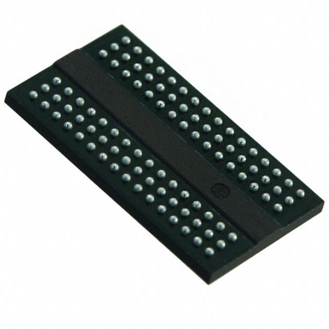
AS4C64M16D3LA-12BAN 96 ball FBGA PACKAGE
Revision
Rev 1.0
Details
Preliminary datasheet
Date
Aug. 2016
Alliance Memory Inc. 511 Taylor Way, San Carlos, CA 94070 TEL: (650) 610-6800 FAX: (650) 620-9211
Alliance Memory Inc. reserves the right to change products or specification without notice
Confidential
- 1/86 -
Rev.1.0 Aug.2016
�AS4C64M16D3LA-12BAN
Features
Overview
JEDEC Standard Compliant
Power supplies: VDD & VDDQ = +1.35V
Backward compatible to VDD & VDDQ = 1.5V ±0.075V
Automotive temperature: -40~105°C (TC)
AEC-Q100 Compliant
Supports JEDEC clock jitter specification
Fully synchronous operation
Fast clock rate: 800MHz
Differential Clock, CK & CK#
Bidirectional differential data strobe
- DQS & DQS#
8 internal banks for concurrent operation
8n-bit prefetch architecture
Pipelined internal architecture
Precharge & active power down
Programmable Mode & Extended Mode registers
Additive Latency (AL): 0, CL-1, CL-2
Programmable Burst lengths: 4, 8
Burst type: Sequential / Interleave
Output Driver Impedance Control
8192 refresh cycles / 64ms
- Average refresh period
7.8μs @ -40°C ≦TC≦ +85°C
3.9μs @ +85°C <TC≦ +105°C
Write Leveling
ZQ Calibration
Dynamic ODT (Rtt_Nom & Rtt_WR)
RoHS compliant
Auto Refresh and Self Refresh
96-ball 8 x 13 x 1.0mm FBGA package
- Pb and Halogen Free
The 1Gb Double-Data-Rate-3 (DDR3L) DRAMs is
double data rate architecture to achieve high-speed
operation. It is internally configured as an eight bank
DRAM.
The 1Gb chip is organized as 8Mbit x 16 I/Os x 8
bank devices. These synchronous devices achieve high
speed double-data-rate transfer rates of up to 1600
Mb/sec/pin for general applications.
The chip is designed to comply with all key DDR3L
DRAM key features and all of the control and address
inputs are synchronized with a pair of externally supplied
differential clocks. Inputs are latched at the cross point
of differential clocks (CK rising and CK# falling). All I/Os
are synchronized with differential DQS pair in a source
synchronous fashion.
These devices operate with a single 1.35V -0.067V
/+0.1V power supply and are available in BGA packages.
Table 1. Ordering Information
Product part No
AS4C64M16D3LA-12BAN
Org
Temperature
Max Clock (MHz)
Package
800
96-ball FBGA
64M x 16 Automotive -40°C to 105°C
Table 2. Speed Grade Information
Confidential
Speed Grade
Clock Frequency
CAS Latency
tRCD (ns)
tRP (ns)
DDR3L-1600
800 MHz
11
13.75
13.75
- 2/86 -
Rev.1.0 Aug.2016
�AS4C64M16D3LA-12BAN
Figure 1. Ball Assignment (FBGA Top View)
A
1
2
3
VDDQ
DQ13
B
VSSQ
C
…
7
8
9
DQ15
DQ12
VDDQ
VSS
VDD
VSS
UDQS#.
DQ14
VSSQ
VDDQ
DQ11
DQ9
UDQS
DQ10
VDDQ
D
VSSQ
VDDQ
UDM
DQ8
VSSQ
VDD
E
VSS
VSSQ
DQ0
LDM
VSSQ
VDDQ
F
VDDQ
DQ2
LDQS
DQ1
DQ3
VSSQ
G
VSSQ
DQ6
LDQS#
VDD
VSS
VSSQ
H
VREFDQ
VDDQ
DQ4
DQ7
DQ5
VDDQ
J
NC
VSS
RAS#
CK
VSS
NC
K
ODT
VDD
CAS#
CK#
VDD
CKE
L
NC
CS#
WE#
A10/AP
ZQ
NC
M
VSS
BA0
BA2
NC
VREFCA
VSS
N
VDD
A3
A0
A12/BC#
BA1
VDD
P
VSS
A5
A2
A1
A4
VSS
R
VDD
A7
A9
A11
A6
VDD
T
VSS
RESET#
NC
NC
A8
VSS
Confidential
- 3/86 -
Rev.1.0 Aug.2016
�AS4C64M16D3LA-12BAN
Figure 2. Block Diagram
CK
CK#
CKE
Row
Decoder
DLL
CLOCK
BUFFER
8M x 16
CELL ARRAY
(BANK #0)
Column Decoder
CS#
RAS#
CAS#
WE#
Row
Decoder
COMMAND
DECODER
CONTROL
SIGNAL
GENERATOR
Row
Decoder
RESET#
A0
REFRESH
COUNTER
ZQCL
ZQCS
ZQ
CAL
Column Decoder
8M x 16
CELL ARRAY
(BANK #2)
Column Decoder
8M x 16
CELL ARRAY
(BANK #3)
Column Decoder
8M x 16
CELL ARRAY
(BANK #4)
Column Decoder
8M x 16
CELL ARRAY
(BANK #5)
Column Decoder
RZQ
DATA
STROBE
BUFFER
DQ
Buffer
Row
Decoder
LDQS
LDQS#
UDQS
UDQS#
Row
Decoder
~
ADDRESS
BUFFER
A9
A11
A12
BA0
BA1
BA2
VSSQ
MODE
REGISTER
Row
Decoder
COLUMN
COUNTER
Row
Decoder
A10/AP
A12/BC#
8M x 16
CELL ARRAY
(BANK #1)
8M x 16
CELL ARRAY
(BANK #6)
Column Decoder
DQ0
Row
Decoder
~
DQ15
ODT
Confidential
- 4/86 -
LDM
UDM
8M x 16
CELL ARRAY
(BANK #7)
Column Decoder
Rev.1.0 Aug.2016
�AS4C64M16D3LA-12BAN
Figure 3. State Diagram
This simplified State Diagram is intended to provide an overview of the possible state transitions and the commands
to control them. In particular, situations involving more than one bank, the enabling or disabling of on-die termination,
and some other events are not captured in full detail
Power
On
Reset
Procedure
from any
RESET
state
ZQCL
PRE = Precharge
PREA = Precharge All
Self
Refresh
MRS
ZQCL,ZQCS
Active
Power
Down
Idle
REF
ACT
E
PD X
PD
ZQ
Calibration
ACT = Active
MRS,MPR,
Write
Leveling
Initialization
SR
SR E
X
Power
applied
Precharge
Power
Down
Activating
PD
X
MRS = Mode Register Set
PD
E
REF = Refresh
RESET = Start RESET Procedure
Bank
Activating
Read = RD, RDS4, RDS8
Read A = RDA, RDAS4, RDAS8
ZQCS = ZQ Calibration Short
EA
WRITE
RE
Writing
AD
RE
READ A
ITE
WR
A
RE
A
PR
E
Reading
A
RE
,P
EA
PR
Automatic Sequence
Command Sequence
DA
PRE, PREA
E,
PR
Writing
Reading
A
WRITE A
MPR = Multi-Purpose Register
Confidential
READ
READ
WRITE
PDE = Enter Power-down
PDX = Exit Power-down
SRE = Self-Refresh entry
SRX = Self-Refresh exit
AD
WR
IT
TE
ZQCL = ZQ Calibration Long
RI
Write A = WRA, WRAS4, WRAS8
W
Write = WR, WRS4, WRS8
Refreshing
Precharging
- 5/86 -
Rev.1.0 Aug.2016
�AS4C64M16D3LA-12BAN
Ball Descriptions
Table 3. Ball Descriptions
Symbol
Type
Description
CK, CK#
Input
Differential Clock: CK and CK# are driven by the system clock. All SDRAM input signals
are sampled on the crossing of positive edge of CK and negative edge of CK#. Output
(Read) data is referenced to the crossings of CK and CK# (both directions of crossing).
CKE
Input
Clock Enable: CKE activates (HIGH) and deactivates (LOW) the CK signal. If CKE goes
LOW synchronously with clock, the internal clock is suspended from the next clock cycle
and the state of output and burst address is frozen as long as the CKE remains LOW.
When all banks are in the idle state, deactivating the clock controls the entry to the Power
Down and Self Refresh modes.
BA0-BA2
Input
Bank Address: BA0-BA2 define to which bank the BankActivate, Read, Write, or Bank
Precharge command is being applied.
A0-A12
Input
Address Inputs: A0-A12 are sampled during the BankActivate command (row address A0A12) and Read/Write command (column address A0-A9 with A10 defining Auto Precharge).
A10/AP
Input
Auto-Precharge: A10 is sampled during Read/Write commands to determine whether
Autoprecharge should be performed to the accessed bank after the Read/Write operation.
(HIGH: Autoprecharge; LOW: no Autoprecharge). A10 is sampled during a Precharge
command to determine whether the Precharge applies to one bank (A10 LOW) or all banks
(A10 HIGH).
A12/BC#
Input
Burst Chop: A12/BC# is sampled during Read and Write commands to determine if burst
chop (on the fly) will be performed. (HIGH - no burst chop; LOW - burst chopped).
CS#
Input
Chip Select: CS# enables (sampled LOW) and disables (sampled HIGH) the command
decoder. All commands are masked when CS# is sampled HIGH. It is considered part of
the command code.
RAS#
Input
Row Address Strobe: The RAS# signal defines the operation commands in conjunction
with the CAS# and WE# signals and is latched at the crossing of positive edges of CK and
negative edge of CK#. When RAS# and CS# are asserted "LOW" and CAS# is asserted
"HIGH" either the BankActivate command or the Precharge command is selected by the
WE# signal. When the WE# is asserted "HIGH" the BankActivate command is selected and
the bank designated by BA is turned on to the active state. When the WE# is asserted
"LOW" the Precharge command is selected and the bank designated by BA is switched to
the idle state after the precharge operation.
CAS#
Input
Column Address Strobe: The CAS# signal defines the operation commands in
conjunction with the RAS# and WE# signals and is latched at the crossing of positive edges
of CK and negative edge of CK#. When RAS# is held "HIGH" and CS# is asserted "LOW"
the column access is started by asserting CAS# "LOW". Then, the Read or Write command
is selected by asserting WE# “HIGH" or “LOW".
WE#
Input
Write Enable: The WE# signal defines the operation commands in conjunction with the
RAS# and CAS# signals and is latched at the crossing of positive edges of CK and negative
edge of CK#. The WE# input is used to select the BankActivate or Precharge command
and Read or Write command.
LDQS,
LDQS#
UDQS
UDQS#
LDM,
UDM
Confidential
Input / Bidirectional Data Strobe: Specifies timing for Input and Output data. Read Data Strobe is
edge triggered. Write Data Strobe provides a setup and hold time for data and DQM. LDQS
Output
is for DQ0~7, UDQS is for DQ8~15. The data strobes LDOS and UDQS are paired with
LDQS# and UDQS# to provide differential pair signaling to the system during both reads
and writes.
Input
Data Input Mask: Input data is masked when DM is sampled HIGH during a write cycle.
LDM masks DQ0-DQ7, UDM masks DQ8-DQ15.
- 6/86 -
Rev.1.0 Aug.2016
�AS4C64M16D3LA-12BAN
DQ0 - DQ15
Input / Data I/O: The The data bus input and output data are synchronized with positive and
Output negative edges of DQS/DQS#. TheI/Os are byte-maskable during Writes.
ODT
Input
On Die Termination: ODT (registered HIGH) enables termination resistance internal to the
DDR3L SDRAM. When enabled, ODT is applied to each DQ, DQS, DQS#. The ODT pin
will be ignored if Mode-registers, MR1and MR2, are programmed to disable RTT.
RESET#
Input
Active Low Asynchronous Reset: Reset is active when RESET# is LOW, and inactive
when RESET# is HIGH. RESET# must be HIGH during normal operation. RESET# is a
CMOS rail to rail signal with DC high and low at 80% and 20% of VDD
VDD
Supply Power Supply: 1.35V -0.067V/+0.1V.
VSS
Supply Ground
VDDQ
Supply DQ Power: 1.35V -0.067V/+0.1V.
VSSQ
Supply DQ Ground
VREFCA
Supply Reference voltage for CA
VREFDQ
Supply Reference voltage for DQ
ZQ
NC
Confidential
Supply Reference pin for ZQ calibration.
-
No Connect: These pins should be left unconnected.
- 7/86 -
Rev.1.0 Aug.2016
�AS4C64M16D3LA-12BAN
Operation Mode Truth Table
Command
Table 4. Truth Table (Note (1), (2))
State CKEn-1(3) CKEn DM BA0-2 A10/AP A0-9, 11 A12/BC# CS# RAS# CAS# WE#
Idle(4)
H
H
X
V
Single Bank Precharge
Any
H
H
X
V
L
V
All Banks Precharge
Any
H
H
X
V
H
V
Write (Fixed BL8 or BC4)
Active(4)
H
H
X
V
L
Write (BC4, on the fly)
Active(4)
H
H
X
V
Write (BL8, on the fly)
Active(4)
H
H
X
Write with Autoprecharge
Active(4)
H
H
Active(4)
H
Active(4)
Read (Fixed BL8 or BC4)
L
L
H
H
V
L
L
H
L
V
L
L
H
L
V
V
L
H
L
L
L
V
L
L
H
L
L
V
L
V
H
L
H
L
L
X
V
H
V
V
L
H
L
L
H
X
V
H
V
L
L
H
L
L
H
H
X
V
H
V
H
L
H
L
L
Active(4)
H
H
X
V
L
V
V
L
H
L
H
Read (BC4, on the fly)
Active(4)
H
H
X
V
L
V
L
L
H
L
H
Read (BL8, on the fly)
Active(4)
H
H
X
V
L
V
H
L
H
L
H
Read with Autoprecharge
Active(4)
H
H
X
V
H
V
V
L
H
L
H
Active(4)
H
H
X
V
H
V
L
L
H
L
H
Active(4)
H
H
X
V
H
V
H
L
H
L
H
(Extended) Mode Register Set
Idle
H
H
X
V
L
L
L
L
No-Operation
Any
H
H
X
V
V
V
V
L
H
H
H
Device Deselect
Any
H
H
X
X
X
X
X
H
X
X
X
Refresh
Idle
H
H
X
V
V
V
V
L
L
L
H
SelfRefresh Entry
Idle
H
L
X
V
V
V
V
L
L
L
H
SelfRefresh Exit
Idle
L
H
X
X
X
X
X
H
X
X
X
V
V
V
V
L
H
H
H
Power Down Mode Entry
Idle
H
L
X
X
X
X
X
H
X
X
X
V
V
V
V
L
H
H
H
X
X
X
X
H
X
X
X
V
V
V
V
L
H
H
H
X
X
X
X
X
X
X
BankActivate
(Fixed BL8 or BC4)
Write with Autoprecharge
(BC4, on the fly)
Write with Autoprecharge
(BL8, on the fly)
(Fixed BL8 or BC4)
Read with Autoprecharge
(BC4, on the fly)
Read with Autoprecharge
(BL8, on the fly)
Row address
OP code
Power Down Mode Exit
Any
L
H
X
Data Input Mask Disable
Active
H
X
L
X
Data Input Mask Enable(5)
Active
H
X
H
X
X
X
X
X
X
X
X
Idle
H
H
X
X
H
X
X
L
H
H
L
X
L
H
H
L
ZQ Calibration Long
Idle
H
H
X
X
L
X
NOTE 1: V=Valid data, X=Don't Care, L=Low level, H=High level
NOTE 2: CKEn signal is input level when commands are provided.
NOTE 3: CKEn-1 signal is input level one clock cycle before the commands are provided.
NOTE 4: These are states of bank designated by BA signal.
NOTE 5: LDM and UDM can be enabled respectively.
ZQ Calibration Short
Confidential
- 8/86 -
Rev.1.0 Aug.2016
�AS4C64M16D3LA-12BAN
Functional Description
The DDR3L SDRAM is a high-speed dynamic random access memory internally configured as an eight-bank
DRAM. The DDR3L SDRAM uses an 8n prefetch architecture to achieve high speed operation. The 8n Prefetch
architecture is combined with an interface designed to transfer two data words per clock cycle at the I/O pins. A
single read or write operation for the DDR3L SDRAM consists of a single 8n-bit wide, four clock data transfer at the
internal DRAM core and two corresponding n-bit wide, one-half clock cycle data transfers at the I/O pins.
Read and write operation to the DDR3L SDRAM are burst oriented, start at a selected location, and continue for a
burst length of eight or a ‘chopped’ burst of four in a programmed sequence. Operation begins with the registration
of an Active command, which is then followed by a Read or Write command. The address bits registered coincident
with the Active command are used to select the bank and row to be activated (BA0-BA2 select the bank; A0-A12
select the row). The address bit registered coincident with the Read or Write command are used to select the
starting column location for the burst operation, determine if the auto precharge command is to be issued (via A10),
and select BC4 or BL8 mode ‘on the fly’ (via A12) if enabled in the mode register.
Prior to normal operation, the DDR3L SDRAM must be powered up and initialized in a predefined manner. The
following sections provide detailed information covering device reset and initialization, register definition, command
descriptions and device operation.
Figure 4. Reset and Initialization Sequence at Power-on Ramping
CK#
Ta
Tb
CK
VDD
VDDQ
Tc
Td
Te
Tf
Tg
Th
Ti
Tk
Tj
tCKSRX
T=200μs
T=500μs
RESET#
Tmin=10ns
tIS
CKE
tDLLK
tIS
COMMAND
Note 1
BA
tXPR
tMRD
tMRD
tMRD
tMOD
MRS
MRS
MRS
MRS
MR2
MR3
MR1
MR0
tZQinit
ZQCL
Note 1
VALID
tIS
ODT
VALID
tIS
Static LOW in case RTT_Nom is enabled at time Tg, otherwise static HIGH or LOW
VALID
RTT
NOTE 1. From time point "Td" until "Tk " NOP or DES commands must be applied between MRS and ZQCL commands.
TIME BREAK
Confidential
- 9/86 -
Don't Care
Rev.1.0 Aug.2016
�AS4C64M16D3LA-12BAN
Power-up and Initialization
The Following sequence is required for POWER UP and Initialization
1. Apply power (RESET# is recommended to be maintained below 0.2 x VDD, all other inputs may be undefined).
RESET# needs to be maintained for minimum 200us with stable power. CKE is pulled “Low” anytime before
RESET# being de-asserted (min. time 10ns). The power voltage ramp time between 300mV to VDDmin must be
no greater than 200ms; and during the ramp, VDD>VDDQ and (VDD-VDDQ) VIH(ac)=VREF(dc)+135mV, VIL(ac)=VREF(dc)-135mV
DQS, DQS# Differential Slew Rate
4.0 V/ns
DQ
Slew
Rate
V/ns
Confidential
2.0
1.5
1.0
0.9
0.8
0.7
0.6
0.5
0.4
3.0 V/ns
2.0 V/ns
1.8 V/ns
1.6 V/ns
1.4 V/ns
1.2 V/ns
1.0 V/ns
△ tDS
△ tDH
△ tDS
△ tDH
△ tDS
△ tDH
△ tDS
△ tDH
△ tDS
△ tDH
△ tDS
△ tDH
△ tDS
△ tDH
△ tDS
△ tDH
68
45
0
-
45
30
0
-
68
45
0
2
-
45
30
0
-3
-
68
45
0
2
3
-
45
30
0
-3
-8
-
53
8
10
11
14
-
38
8
5
1
-5
-
16
18
19
22
25
-
16
13
9
3
-4
-
26
27
30
33
29
-
21
17
11
4
-6
-
35
38
41
37
30
27
21
14
4
-11
46
49
45
38
37
30
20
5
- 60/86 -
Rev.1.0 Aug.2016
�AS4C64M16D3LA-12BAN
Timing Waveforms
Figure 25. MPR Readout of predefined pattern,BL8 fixed burst order, single readout
T0
Ta
Tb0
Tb1
Tc0
Tc1
Tc2
Tc3
Tc4
Tc5
Tc6
PREA
MRS
READ
NOP
NOP
NOP
NOP
NOP
NOP
NOP
NOP
CK#
CK
Tc7
Tc8
Tc9
tMPRR
COMMAND
tRP
tMOD
Td
tMOD
MRS
MRS
MRS
VALID
Notes 1
BA
3
VALID
3
A[1:0]
0
0
VALID
Notes 2
A[2]
1
0
0
Notes 2
A[9:3]
00
VALID
00
0
VALID
0
A[11]
0
VALID
0
A12, BC#
0
VALID
0
A[15:13]
0
VALID
A10, AP
1
0
RL
DQS, DQS#
DQ
NOTES:
1.
2.
BL8 either by MRS or OTF.
er must drive 0 on A[2:0].
TIME BREAK
Don't Care
Figure 26. MPR Readout of predefined pattern,BL8 fixed burst order, back to back readout
CK#
T0
Ta
Tb
Tc0
Tc1
Tc2
Tc3
Tc4
Tc5
Tc6
Tc7
PREA
MRS
READ
READ
NOP
NOP
NOP
NOP
NOP
NOP
NOP
Tc8
Tc9
CK
COMMAND
Tc10
tMPRR
tRP
tMOD
Notes 1
tCCD
NOP
NOP
tMOD
MRS
3
VALID
VALID
3
A[1:0]
0
0
0
VALID
A[2]
1
Notes 2
0
0
0
Notes 2
Notes 2
A[9:3]
00
VALID
VALID
00
0
VALID
VALID
0
A[11]
0
VALID
VALID
0
A12, BC#
0
VALID
VALID
0
A10, AP
1
Notes 1
Notes 1
A[15:13]
0
VALID
Notes 1
BA
Notes 2
Td
VALID
VALID
0
RL
DQS, DQS#
RL
DQ
NOTES:
1.
th BL8 either by MRS or OTF.
2.
ler must drive 0 on A[2:0].
Confidential
TIME BREAK
- 61/86 -
Don't Care
Rev.1.0 Aug.2016
�AS4C64M16D3LA-12BAN
Figure 27. MPR Readout of predefined pattern,BC4 lower nibble then upper nibble
CK#
T0
Ta
Tb
Tc0
Tc1
Tc2
Tc3
Tc4
Tc5
Tc6
Tc7
PREA
MRS
READ
READ
NOP
NOP
NOP
NOP
NOP
NOP
NOP
CK
COMMAND
Tc8
tMPRR
tRP
tMOD
tCCD
VALID
VALID
3
A[1:0]
0
0
0
VALID
Notes 2
1
0
1
VALID
00
0
VALID
VALID
0
A[11]
0
VALID
VALID
0
A12, BC#
0
VALID
VALID
0
Notes 1
Notes 1
0
VALID
VALID
0
VALID
A[15:13]
NOP
Notes 4
00
1
NOP
Notes 2
Notes 3
A[9:3]
Td
Notes 1
Notes 1
3
A[2]
Tc10
tMOD
MRS
BA
A10, AP
Tc9
VALID
0
RL
DQS, DQS#
RL
DQ
NOTES:
1.
th BC4 either by MRS or OTF.
2.
ler must drive 0 on A[1:0].
3.
selects lower 4 nibble bits 0....3.
4.
selects upper 4 nibble bits 4....7.
TIME BREAK
Don't Care
Figure 28. MPR Readout of predefined pattern,BC4 upper nibble then lower nibble
CK#
T0
Ta
Tb
Tc0
Tc1
Tc2
Tc3
Tc4
Tc5
Tc6
Tc7
PREA
MRS
READ
READ
NOP
NOP
NOP
NOP
NOP
NOP
NOP
CK
COMMAND
Tc8
tMPRR
tRP
tMOD
Notes 1
tCCD
VALID
VALID
3
A[1:0]
0
0
0
VALID
A[2]
1
1
0
VALID
00
0
VALID
VALID
0
A[11]
0
VALID
VALID
0
A12, BC#
0
VALID
VALID
0
Notes 1
Notes 1
0
VALID
VALID
0
VALID
A[15:13]
NOP
Notes 3
00
1
NOP
Notes 2
Notes 4
A[9:3]
Td
Notes 1
3
Notes 2
Tc10
tMOD
MRS
BA
A10, AP
Tc9
VALID
0
RL
DQS, DQS#
RL
DQ
NOTES:
1.
th BC4 either by MRS or OTF.
2.
ler must drive 0 on A[1:0].
3. 2]=0 selects lower 4 nibble bits 0....3.
4. 2]=1 selects upper 4 nibble bits 4....7.
Confidential
TIME BREAK
- 62/86 -
Don't Care
Rev.1.0 Aug.2016
�AS4C64M16D3LA-12BAN
Figure 29. READ (BL8) to READ (BL8)
CK#
CK
T0
T1
T2
T3
T4
T5
T6
T7
T8
T9
T10
READ
NOP
NOP
NOP
READ
NOP
NOP
NOP
NOP
NOP
NOP
T11
T12
T13
T14
NOP
NOP
NOP
Notes 3
COMMAND
ADDRESS
NOP
tCCD
Notes 4
Bank,
Col n
Bank,
Col b
tRPRE
tRPST
DQS, DQS#
Notes 2
DQ
Dout
n
RL = 5
Dout
n+1
Dout
n+2
Dout
n+3
Dout
n+4
Dout
n+5
Dout
n+6
Dout
n+7
Dout
b
Dout
b+1
Dout
b+2
Figure 30. Nonconsecutive READ (BL8) to READ (BL8)
CK
T0
T1
T2
READ
NOP
NOP
Dout
b+4
Dout
b+5
Dout
b+6
Dout
b+7
RL = 5
TRANSITIONING DATA
NOTES:
1. BL8, RL = 5 (CL = 5, AL = 0)
2. DOUT n (or b) = data-out from column n (or column b).
3. NOP commands are shown for ease of illustration; other commands may be valid at these times.
4. BL8 setting activated by either MR0[A1:0 = 00] or MR0[A1:0 = 01] and A12 = 1 during READ commands at T0 and T4.
CK#
Dout
b+3
Don't Care
T3
T4
T5
T6
T7
T8
T9
T10
T11
T12
T13
NOP
NOP
READ
NOP
NOP
NOP
NOP
NOP
NOP
NOP
NOP
T14
Notes 3
COMMAND
ADDRESS
NOP
tCCD = 5
Notes 4
Bank,
Col n
Bank,
Col b
tRPRE
Notes 5
tRPST
DQS, DQS#
Notes 2
DQ
DO
n
RL = 5
NOTES:
1.
2.
3.
4.
5.
RL = 5
= 5, AL = 0), tCCD=5
) = data-out from column n (or column b)
nds are shown for ease of illustration; other commands may be valid at these times
ing activated by either MR0[A1:0 = 00] or MR0[A1:0 = 01] and A12 = 1 during READ commands at T0 and T4
logic low at T9
Figure 31. READ (BL4) to READ (BL4)
CK#
CK
DO
b
T0
T1
T2
READ
NOP
NOP
T3
T4
NOP
READ
T5
T6
T7
T8
T9
TRANSITIONING DATA
T10
T11
T12
T13
NOP
NOP
NOP
NOP
Don't Care
T14
Notes 3
COMMAND
ADDRESS
NOP
NOP
NOP
NOP
NOP
NOP
tCCD
Notes 4
Bank,
Col n
Bank,
Col b
tRPST
tRPRE
tRPST
tRPRE
DQS, DQS#
Notes 2
DQ
RL = 5
Dout
n
Dout
n+1
Dout
n+2
Dout
n+3
Dout
b
Dout
b+1
Dout
b+3
RL = 5
NOTES:
1.
5 (CL = 5, AL = 0)
2.
(or b) = data-out from column n (or column b).
3.
nds are shown for ease of illustration; other commands may be valid at these times.
4.
tting activated by either MR0[A1:0 = 10] or MR0[A1:0 = 01] and A12 = 0 during READ commands at T0 and T4.
Confidential
Dout
b+2
- 63/86 -
TRANSITIONING DATA
Don't Care
Rev.1.0 Aug.2016
�AS4C64M16D3LA-12BAN
Figure 32. READ (BL8) to WRITE (BL8)
T0
T1
T2
READ
NOP
NOP
CK#
CK
T3
T4
T5
T6
T7
T8
T9
T10
T11
T12
T13
NOP
NOP
READ
NOP
NOP
NOP
NOP
NOP
NOP
NOP
NOP
T14
Notes 3
COMMAND
NOP
tCCD = 5
Notes 4
Bank,
Col n
ADDRESS
Bank,
Col b
tRPRE
Notes 5
tRPST
DQS, DQS#
Notes 2
DQ
DO
n
RL = 5
NOTES:
1.
2.
3.
4.
5.
DO
b
RL = 5
= 5, AL = 0), tCCD=5
) = data-out from column n (or column b)
nds are shown for ease of illustration; other commands may be valid at these times
ing activated by either MR0[A1:0 = 00] or MR0[A1:0 = 01] and A12 = 1 during READ commands at T0 and T4
logic low at T9
Figure 33. READ (BL4) to WRITE (BL4) OTF
CK#
T0
T1
T2
T3
T4
T5
READ
NOP
NOP
NOP
WRITE
T6
T7
T8
T9
TRANSITIONING DATA
T10
T11
T12
T13
NOP
NOP
NOP
NOP
Don't Care
T14
T15
CK
Notes 3
COMMAND
NOP
NOP
NOP
NOP
NOP
NOP
NOP
tWR
4 clocks
READ to WRITE Command Delay = RL + tCCD/2 + 2tCK - WL
Notes 4
ADDRESS
Bank,
Col n
Bank,
Col b
tWPST
tWPRE
tRPST
tRPRE
tWTR
DQS, DQS#
DQ
Notes 2
Dout
n
RL = 5
Dout
n+1
Dout
n+2
Dout
n+3
Din
b
Din
b+1
Din
b+2
Din
b+3
WL = 5
NOTES:
1.
= 5 (CL = 5, AL = 0), WL = 5 (CWL = 5, AL = 0)
2.
n = data-out from column, DIN b = data-in from column b.
3.
commands are shown for ease of illustration; other commands may be valid at these times.
4.
setting activated by MR0[A1:0 = 01] and A12 = 0 during READ command at T0 and WRITE command at T4.
Figure 34. READ (BL8) to READ (BL4) OTF
CK#
T0
T1
READ
NOP
T2
T3
NOP
NOP
TRANSITIONING DATA
T4
T5
T6
T7
T8
T9
T10
T11
READ
NOP
NOP
NOP
NOP
NOP
NOP
NOP
Don't Care
T12
T13
NOP
NOP
T14
CK
Notes 3
COMMAND
Notes 4
ADDRESS
NOP
tCCD
Bank,
Col n
Bank,
Col b
tRPST
tRPRE
DQS, DQS#
Notes 2
DQ
RL = 5
Dout
n
Dout
n+1
Dout
n+2
Dout
n+3
Dout
n+5
Dout
n+6
Dout
n+7
Dout
b
Dout
b+1
Dout
b+2
Dout
b+3
RL = 5
NOTES:
1.
= 5 (CL = 5, AL = 0)
2.
(or b) = data-out from column n (or column b).
3.
n for ease of illustration; other commands may be valid at these times.
4.
setting activated by MR0[A1:0 = 01] and A12 = 1 during READ command at T0.
BC4 setting activated by MR0[A1:0 = 01] and A12 = 0 during READ command at T4.
Confidential
Dout
n+4
- 64/86 -
TRANSITIONING DATA
Don't Care
Rev.1.0 Aug.2016
�AS4C64M16D3LA-12BAN
Figure 35. READ (BL4) to READ (BL8) OTF
CK#
T0
T1
READ
NOP
T2
T3
T4
NOP
NOP
READ
T5
T6
T7
T8
T9
T10
T11
T12
T13
NOP
NOP
NOP
NOP
T14
CK
Notes 3
COMMAND
NOP
NOP
NOP
NOP
NOP
NOP
tCCD
Notes 4
ADDRESS
Bank,
Col n
Bank,
Col b
tRPST
tRPRE
tRPST
tRPRE
DQS, DQS#
Notes 2
DQ
Dout
n
RL = 5
Dout
n+1
Dout
n+2
Dout
n+3
Dout
b
Dout
b+1
Dout
b+2
Dout
b+3
Dout
b+5
Dout
b+6
Dout
b+7
RL = 5
NOTES:
1.
5 (CL = 5, AL = 0)
2.
n (or b) = data-out from column n (or column b).
3.
commands are shown for ease of illustration; other commands may be valid at these times.
4.
4 setting activated by MR0[A1:0 = 01] and A12 = 0 during READ command at T0.
BL8 setting activated by MR0[A1:0 = 01] and A12 = 1 during READ command at T4.
Figure 36. READ (BC4) to WRITE (BL8) OTF
CK#
Dout
b+4
T0
T1
T2
T3
T4
READ
NOP
NOP
NOP
WRITE
T5
T6
TRANSITIONING DATA
T7
T8
T9
T10
T11
T12
T13
NOP
NOP
NOP
NOP
Don't Care
T14
T15
CK
Notes 3
COMMAND
NOP
NOP
NOP
NOP
NOP
NOP
NOP
tWR
4 clocks
READ to WRITE Command Delay = RL + tCCD/2 + 2tCK - WL
Notes 4
ADDRESS
Bank,
Col n
tWTR
Bank,
Col b
tWPST
tWPRE
tRPST
tRPRE
DQS, DQS#
DQ
Notes 2
Dout
n
RL = 5
Dout
n+1
Dout
n+2
Dout
n+3
Din
b
Din
b+1
Din
b+2
Din
b+3
Din
b+4
NOTES:
1.
= 5 (CL = 5, AL = 0), WL = 5 (CWL = 5, AL = 0)
2.
n = data-out from column, DIN b = data-in from column b.
3.
commands are shown for ease of illustration; other commands may be valid at these times.
4.
setting activated by MR0[A1:0 = 01] and A12 = 0 during READ command at T0 and WRITE command at T4.
Figure 37. READ (BL8) to WRITE (BL4) OTF
CK#
Din
b+5
Din
b+6
Din
b+7
WL = 5
T0
T1
T2
T3
T4
READ
NOP
NOP
NOP
NOP
T5
T6
T7
TRANSITIONING DATA
T8
T9
T10
T11
T12
T13
NOP
NOP
NOP
NOP
Don't Care
T14
T15
NOP
NOP
CK
Notes 3
COMMAND
NOP
WRITE
NOP
NOP
NOP
tWR
READ to WRITE Command Delay = RL + tCCD + 2tCK - WL
Notes 4
ADDRESS
4 clocks
Bank,
Col n
tWTR
Bank,
Col b
tRPST
tRPRE
tWPST
tWPRE
DQS, DQS#
DQ
Notes 2
RL = 5
Dout
n
Dout
n+1
Dout
n+2
Dout
n+3
Dout
n+4
Dout
n+6
Dout
n+7
Din
b
Din
b+1
Din
b+2
Din
b+3
WL = 5
NOTES:
1.
= 5 (CL = 5, AL = 0), WL = 5 (CWL= 5, AL = 0)
2.
n = data-out from column, DIN b = data-in from column b.
3.
commands are shown for ease of illustration; other commands may be valid at these times.
4.
8 setting activated by MR0[A1:0 = 01] and A12 = 1 during READ command at T0.
BC4 setting activated by MR0[A1:0 = 01] and A12 = 0 during WRITE command at T6.
Confidential
Dout
n+5
- 65/86 -
TRANSITIONING DATA
Don't Care
Rev.1.0 Aug.2016
�AS4C64M16D3LA-12BAN
Figure 38. READ to PRECHARGE, RL = 5, AL = 0, CL = 5, tRTP = 4, tRP = 5
CK#
T0
T1
T2
NOP
READ
NOP
T3
T4
NOP
NOP
T5
T6
T7
T8
T9
T10
T11
T12
T13
ACT
NOP
NOP
NOP
T14
T15
NOP
NOP
CK
COMMAND
PRE
NOP
NOP
NOP
NOP
tRP
tRTP
RL = AL + CL
Bank a,
Col n
ADDRESS
DQS, DQS#
Bank a,
all)
Bank a,
Row b
BL4 Operation:
DQ
DQS, DQS#
DO
n
DO
n+1
DO
n+2
DO
n+3
DO
n
DO
n+1
DO
n+2
DO
n+3
BL8 Operation:
DQ
DO
n+4
DO
n+5
DO
n+6
DO
n+7
NOTES:
1.
= 5 (CL = 5, AL = 0)
2.
n = data-out from column n.
3.
commands are shown for ease of illustration; other commands may be valid at these times.
4. he example assumes tRAS.MIN is satisfied at Precharge command time (T5) and that tRC.MIN is satisfied at the next Active command time (T10).
TRANSITIONING DATA
Figure 39. READ to PRECHARGE, RL = 8, AL = CL-2, CL = 5, tRTP = 6, tRP = 5
CK#
T0
T1
T2
T3
T4
NOP
READ
NOP
NOP
NOP
T5
T6
T7
T8
T9
T10
T11
T12
PRE
NOP
NOP
T13
Don't Care
T14
T15
NOP
ACT
CK
COMMAND
AL = CL - 2 = 3
NOP
NOP
NOP
NOP
NOP
tRTP
NOP
tRP
CL = 5
ADDRESS
DQS, DQS#
Bank a,
Col n
Bank a,
all)
BL4 Operation:
DQ
DQS, DQS#
DO
n
DO
n+1
DO
n+2
DO
n+3
DO
n
DO
n+1
DO
n+2
DO
n+3
BL8 Operation:
DQ
NOTES:
1.
= 8 (CL = 5, AL = CL - 2)
2.
n = data-out from column n.
3.
commands are shown for ease of illustration; other commands may be valid at these times.
4. he example assumes tRAS.MIN is satisfied at Precharge command time (T10) and that tRC.MIN is satisfied at the next Active command time (T15).
Confidential
Bank a,
Row b
- 66/86 -
DO
n+4
DO
n+5
DO
n+6
DO
n+7
TRANSITIONING DATA
Don't Care
Rev.1.0 Aug.2016
�AS4C64M16D3LA-12BAN
Figure 40. Write Timing Definition and parameters
CK#
T0
T1
T2
T3
T4
WRITE
NOP
NOP
NOP
NOP
T5
T6
T7
T8
T9
T10
CK
Notes 3
COMMAND
NOP
NOP
NOP
NOP
NOP
WL = AL + CWL
Notes 4
ADDRESS
NOP
Bank
Col n
tDQSS(min)
tWPRE(min)
tDQSS tDSH
tDSH
tDSH
tDSH tWPST(min)
DQS, DQS#
tDQSH(min) tDQSL
tDQSL
tDQSH
DQ
tDQSH
Din
n
tDQSH
tDQSL
tDSS
tDSS
Notes 2
tDQSL
tDSS
Din
n+2
Din
n+4
Din
n+3
tDQSH
tDSS
Din
n+6
tDQSL(min)
tDSS
Din
n+7
DM
tDQSS(nominal)
tDSH
tWPRE(min)
tDSH
tDSH
tDSH
tWPST(min)
DQS, DQS#
tDQSH(min) tDQSL
tDQSH
tDSS
Notes 2
DQ
tDQSL
tDSS
Din
n
tDQSH
Din
n+2
tDQSL
tDSS
tDQSH
tDQSL
Din
n+4
Din
n+3
tDQSH tDQSL(min)
tDSS
tDSS
Din
n+6
Din
n+7
DM
tDQSS(max)
tDQSS
tWPRE(min)
tDSH
tDSH
tDSH
tDSH
tWPST(min)
DQS, DQS#
tDQSH(min) tDQSL
Notes 2
tDQSH
tDSS
DQ
tDQSL
tDQSH
tDSS
Din
n
tDQSL
tDQSH
tDSS
Din
n+2
Din
n+3
tDQSH tDQSL(min)
tDQSL
tDSS
Din
n+4
tDSS
Din
n+6
Din
n+7
DM
NOTES:
1.
= 5 (AL = 0, CWL = 5)
2.
= data-in from column n.
3.
commands are shown for ease of illustration; other commands may be valid at these times.
4.
tting activated by either MR0[A1:0 = 00] or MR0[A1:0 = 01] and A12 = 1 during WRITE command at T0.
5.
must be met at each rising clock edge.
TRANSITIONING DATA
Confidential
- 67/86 -
Don't Care
Rev.1.0 Aug.2016
�AS4C64M16D3LA-12BAN
Figure 41. WRITE Burst Operation WL = 5 (AL = 0, CWL = 5, BL8)
CK#
T0
T1
T2
T3
T4
WRITE
NOP
NOP
NOP
NOP
T5
T6
T7
T8
T9
T10
CK
Notes 3
COMMAND
NOP
NOP
NOP
NOP
NOP
NOP
WL = AL + CWL
Notes 4
ADDRESS
Bank,
Col n
tWPST
tWPRE
DQS, DQS#
DQ
Notes 2
Din
n
Din
n+1
Din
n+2
Din
n+3
Din
n+4
Din
n+5
Din
n+6
Din
n+7
NOTES:
1.
8, WL = 5; AL = 0, CWL = 5.
2.
= data-in from column n.
3.
commands are shown for ease of illustration; other commands may be valid at these times.
4.
8 setting activated by either MR0[A1:0 = 00] or MR0[A1:0 = 01] and A12 = 1 during WRITE command at T0.
TRANSITIONING DATA
Figure 42. WRITE Burst Operation WL = 9 (AL = CL-1, CWL = 5, BL8)
CK#
T0
T1
T2
T3
T4
WRITE
NOP
NOP
NOP
NOP
T5
T6
T7
T8
Don't Care
T9
T10
CK
Notes 3
COMMAND
Notes 4
ADDRESS
NOP
NOP
NOP
NOP
NOP
NOP
Bank,
Col n
tWPRE
DQS, DQS#
DQ
Notes 2
Din
n
CWL = 5
AL = 4
Din
n+1
Din
n+2
Din
n+3
WL = AL + CWL
NOTES:
1.
8, WL = 9; AL = (CL - 1), CL = 5, CWL = 5.
2.
= data-in from column n.
3.
commands are shown for ease of illustration; other commands may be valid at these times.
4.
8 setting activated by either MR0[A1:0 = 00] or MR0[A1:0 = 01] and A12 = 1 during WRITE command at T0.
TRANSITIONING DATA
Confidential
- 68/86 -
Don't Care
Rev.1.0 Aug.2016
�AS4C64M16D3LA-12BAN
Figure 43. WRITE(BC4) to READ (BC4) operation
T0
T1
T2
T3
T4
WRITE
NOP
NOP
NOP
NOP
CK#
T5
T6
T7
T8
T9
Tn
CK
Notes 3
COMMAND
NOP
NOP
NOP
NOP
NOP
tWTR
Notes 4
READ
Notes 5
Bank,
Col n
ADDRESS
tWPST
tWPRE
DQS, DQS#
DQ
Notes 2
Din
n
WL = 5
Din
n+1
Din
n+2
Din
n+3
RL = 5
NOTES:
1.
5, RL = 5.
2.
= data-in from column n.
3.
commands are shown for ease of illustration; other commands may be valid at these times.
4.
setting activated by MR0[A1:0 = 10] during WRITE command at T0 and READ command at Tn.
5.
R controls the write to read delay to the same device and starts with the first rising clock edge after the last write data shown at T7.
TRANSITIONING DATA
TIME BREAK
Figure 44. WRITE(BC4) to Precharge Operation
T0
T1
T2
T3
T4
WRITE
NOP
NOP
NOP
NOP
CK#
T5
T6
T7
T8
Don't Care
T9
,
Tn
CK
Notes 3
COMMAND
NOP
NOP
NOP
NOP
NOP
tWR
Notes 4
PRE
Notes 5
Bank,
Col n
ADDRESS
tWPST
tWPRE
DQS, DQS#
DQ
Notes 2
Din
n
WL = 5
Din
n+1
Din
n+2
Din
n+3
NOTES:
1.
5, RL = 5.
2.
= data-in from column n.
3.
commands are shown for ease of illustration; other commands may be valid at these times.
4.
setting activated by MR0[A1:0 = 10] during WRITE command at T0.
5. he write recovery time (tWR) referenced from the first rising clock edge after the last write data shown at T7.
tWR specifies the last burst write cycle until the precharge command can be issued to the same bank .
TIME BREAK
Figure 45. WRITE(BC4) OTF to Precharge operation
CK#
T0
T1
T2
T3
T4
T5
T6
T7
T8
T9
WRITE
NOP
NOP
NOP
NOP
NOP
NOP
NOP
NOP
NOP
TRANSITIONING DATA
T10
Don't Care
T11
Ta0
Ta1
NOP
PRE
NOP
Ta2
CK
Notes 3
COMMAND
NOP
tWR
4 Clocks
Notes 4
ADDRESS
Bank
Col n
NOP
Notes 5
VALID
tWPST
tWPRE
DQS, DQS#
Notes 2
DQ
WL = 5
Din
n
Din
n+1
Din
n+2
Din
n+3
NOTES:
1.
OTF, WL = 5 (CWL = 5, AL = 0)
2.
or b) = data-in from column n.
3.
n for ease of illustration; other commands may be valid at these times.
4.
OTF setting activated by MR0[A1:0 = 01] and A12 = 0 during WRITE command at T0.
5.
write recovery time (tWR) starts at the rising clock edge T9 (4 clocks from T5).
Confidential
- 69/86 -
TIME BREAK
TRANSITIONING DATA
Don't Care
Rev.1.0 Aug.2016
�AS4C64M16D3LA-12BAN
Figure 46. WRITE(BC8) to WRITE(BC8)
CK#
T0
T1
T2
WRITE
NOP
NOP
T3
T4
T5
T6
T7
T8
NOP
WRITE
NOP
NOP
NOP
NOP
T9
T10
T11
T12
T13
NOP
NOP
T14
CK
Notes 3
COMMAND
NOP
NOP
tCCD
NOP
NOP
tWR
tWTR
4 Clocks
Notes 4
ADDRESS
Bank
Col n
Bank
Col b
tWPST
tWPRE
DQS, DQS#
Notes 2
DQ
Din
n
WL = 5
Din
n+1
Din
n+2
Din
n+3
Din
n+4
Din
n+5
Din
n+6
Din
n+7
Din
b
Din
b+1
Din
b+2
Din
b+3
Din
b+4
Din
b+5
Din
b+6
Din
b+7
WL = 5
NOTES:
1. BL8, WL = 5 (CWL = 5, AL = 0)
2. DIN n (or b) = data-in from column n (or column b).
3. NOP commands are shown for ease of illustration; other commands may be valid at these times.
4. BL8 setting activated by either MR0[A1:0 = 00] or MR0[A1:0 = 01] and A12 = 1 during WRITE command at T0 and T4.
5. The write recovery time (tWR) and write timing parameter (tWTR) are referenced from the first rising clock edge after the last write data shown at T13.
TRANSITIONING DATA
Figure 47. WRITE(BC4) to WRITE(BC4) OTF
CK#
T0
T1
T2
WRITE
NOP
NOP
T3
T4
T5
T6
T7
T8
T9
T10
NOP
WRITE
NOP
NOP
NOP
NOP
NOP
NOP
T11
T12
T13
NOP
NOP
Don't Care
T14
CK
Notes 3
COMMAND
tCCD
NOP
NOP
tWR
tWTR
4 Clocks
Notes 4
ADDRESS
Bank
Col n
Bank
Col b
tWPRE
tWPST
tWPRE
tWPST
DQS, DQS#
Notes 2
DQ
Din
n
WL = 5
Din
n+1
Din
n+2
Din
n+3
Din
b
Din
b+1
Din
b+2
Din
b+3
WL = 5
NOTES:
1. BC4, WL = 5 (CWL = 5, AL = 0)
2. DIN n (or b) = data-in from column n (or column b).
3. NOP commands are shown for ease of illustration; other commands may be valid at these times.
4. BC4 setting activated by MR0[A1:0 = 01] and A12 = 0 during WRITE command at T0 and T4.
5. The write recovery time (tWR) and write timing parameter (tWTR) are referenced from the first rising clock edge at T13 (4 clocks from T9).
TRANSITIONING DATA
Figure 48. WRITE(BC8) to READ(BC4,BC8) OTF
CK#
T0
T1
T2
T3
T4
WRITE
NOP
NOP
NOP
NOP
T5
T6
T7
T8
T9
T10
Don't Care
T11
T12
T13
T14
NOP
NOP
READ
NOP
CK
Notes 3
COMMAND
NOP
NOP
NOP
NOP
NOP
NOP
tWTR
Notes 4
ADDRESS
Bank
Col n
tWPST
tWPRE
Bank
Col b
DQS, DQS#
Notes 2
DQ
WL = 5
Din
n
Din
n+1
Din
n+2
Din
n+3
Din
n+4
NOTES:
1. RL = 5 (CL = 5, AL = 0), WL = 5 (CWL = 5, AL = 0)
2. DIN n = data-in from column n; DOUT b = data-out from column b.
3. NOP commands are shown for ease of illustration; other commands may be valid at these times.
4. BL8 setting activated by either MR0[A1:0 = 00] or MR0[A1:0 = 01] and A12 = 1 during WRITE command at T0.
READ command at T13 can be either BC4 or BL8 depending on MR0[A1:0] and A12 status at T13.
Confidential
- 70/86 -
Din
n+5
Din
n+6
RL = 5
Din
n+7
TRANSITIONING DATA
Don't Care
Rev.1.0 Aug.2016
�AS4C64M16D3LA-12BAN
Figure 49. WRITE(BC4) to READ(BC4,BC8) OTF
CK#
T0
T1
T2
T3
T4
T5
T6
WRITE
NOP
NOP
NOP
NOP
NOP
NOP
T7
T8
NOP
NOP
T9
T10
T11
T12
T13
T14
CK
Notes 3
COMMAND
Notes 4
ADDRESS
NOP
NOP
NOP
Bank
Col n
NOP
READ
Bank
Col b
tWPST
tWPRE
NOP
tWTR
4 Clocks
DQS, DQS#
Notes 2
DQ
Din
n
WL = 5
Din
n+1
Din
n+2
RL = 5
Din
n+3
NOTES:
1. L = 5 (CL = 5, AL = 0), WL = 5 (CWL =5, AL = 0)
2. IN n = data-in from column n; DOUT b = data-out from column b.
3. OP commands are shown for ease of illustration; other commands may be valid at these times.
4. C4 setting activated by MR0[A1:0 = 01] and A12 = 0 during WRITE command at T0.
READ command at T13 can be either BC4 or BL8 depending on A12 status at T13.
Figure 50. WRITE(BC4) to READ(BC4)
CK#
TRANSITIONING DATA
T0
T1
T2
T3
T4
T5
T6
T7
T8
WRITE
NOP
NOP
NOP
NOP
NOP
NOP
NOP
NOP
T9
T10
T11
T12
T13
NOP
NOP
Don't Care
T14
CK
Notes 3
COMMAND
Notes 4
ADDRESS
NOP
NOP
READ
NOP
tWTR
Bank
Col n
Bank
Col b
tWPST
tWPRE
DQS, DQS#
Notes 2
RL = 5
DQ
Din
n
WL = 5
Din
n+1
Din
n+2
Din
n+3
NOTES:
1. RL = 5 (CL = 5, AL = 0), WL = 5 (CWL =5, AL = 0)
2. DIN n = data-in from column n; DOUT b = data-out from column b.
3. NOP commands are shown for ease of illustration; other commands may be valid at these times.
4. BC4 setting activated by MR0[A1:0 = 10].
Figure 51. WRITE(BC8) to WRITE(BC4) OTF
CK#
T0
T1
WRITE
NOP
T2
T3
T4
NOP
NOP
WRITE
T5
T6
TRANSITIONING DATA
T7
T8
T9
T10
T11
NOP
NOP
T12
T13
NOP
NOP
Don't Care
T14
CK
Notes 3
COMMAND
NOP
NOP
NOP
NOP
NOP
tCCD
Notes 4
ADDRESS
Bank
Col n
Bank
Col b
NOP
tWR
tWTR
4 Clocks
tWPST
tWPRE
DQS, DQS#
Notes 2
DQ
WL = 5
Din
n
Din
n+1
Din
n+2
Din
n+3
Din
n+5
Din
n+6
Din
n+7
Din
b
Din
b+1
Din
b+2
Din
b+3
WL = 5
NOTES:
1.
= 5 (CWL = 5, AL = 0)
2.
(or b) = data-in from column n (or column b).
3.
commands are shown for ease of illustration; other commands may be valid at these times.
4.
8 setting activated by MR0[A1:0 = 01] and A12 = 1 during WRITE command at T0.
BC4 setting activated by MR0[A1:0 = 01] and A12 = 0 during WRITE command at T4.
Confidential
Din
n+4
- 71/86 -
TRANSITIONING DATA
Don't Care
Rev.1.0 Aug.2016
�AS4C64M16D3LA-12BAN
Figure 52. WRITE(BC4) to WRITE(BC8) OTF
CK#
T0
T1
WRITE
NOP
T2
T3
T4
T5
T6
T7
T8
T9
T10
NOP
NOP
WRITE
NOP
NOP
NOP
NOP
NOP
NOP
T11
T12
T13
NOP
NOP
NOP
T14
CK
Notes 3
COMMAND
tCCD
Notes 4
Bank
Col n
ADDRESS
NOP
tWR
tWTR
4 Clocks
Bank
Col b
tWPRE
tWPST
tWPRE
tWPST
DQS, DQS#
Notes 2
DQ
Din
n
WL = 5
Din
n+1
Din
n+2
Din
n+3
Din
b
Din
b+1
Din
b+2
Din
b+4
Din
b+3
NOTES:
1. WL = 5 (CWL = 5, AL = 0)
2. DIN n (or b) = data-in from column n (or column b).
3. NOP commands are shown for ease of illustration; other commands may be valid at these times.
4. BC4 setting activated by MR0[A1:0 = 01] and A12 = 0 during WRITE command at T0.
BL8 setting activated by MR0[A1:0 = 01] and A12 = 1 during WRITE command at T4.
Figure 53. Refresh Command Timing
CK#
T0
T1
REF
NOP
Din
b+5
Din
b+6
Din
b+7
WL = 5
Ta0
Ta1
REF
NOP
TRANSITIONING DATA
Tb0
Tb1
Tb2
Tb3
VALID
VALID
VALID
VALID
Tc0
Don't Care
Tc1
Tc2
VALID
VALID
Tc3
CK
COMMAND
NOP
NOP
tRFC (min)
tRFC
VALID
REF
VALID
tREFI (max. 9 * tREFI)
DRAM must be idle
DRAM must be idle
NOTES:
1. Only NOP/DES commands allowed after Refresh command registered until tRFC(min) expires.
2. Time interval between two Refresh commands may be extended to a maximum of 9 x tREFI.
Figure 54. Self-Refresh Entry/Exit Timing
T0
T1
T2
Ta0
TIME BREAK
Tb0
Tc0
TRANSITIONING DATA
Tc1
Td0
Don't Care
Teo
Tf0
VALID
VALID
CK#
CK
tCKSRE
tIS
tCKSRX
tCPDED
CKE
tCKESR
tIS
ODT
VALID
ODTL
Notes 1
COMMAND
NOP
SRE
SRX
NOP
NOP
Notes 2
Notes 3
VALID
VALID
VALID
VALID
tXS
ADDR
tRP
tXSDLL
Exit Self
Refresh
Enter Self
Refresh
NOTES:
1. Only NOP or DES command.
2. Valid commands not requiring a locked DLL.
3. Valid commands requiring a locked DLL.
Confidential
TIME BREAK
- 72/86 -
Don't Care
Rev.1.0 Aug.2016
�AS4C64M16D3LA-12BAN
Figure 55. Active Power-Down Entry and Exit Timing Diagram
T0
T1
T2
Ta0
Ta1
Tb0
Tb1
CK#
Tc0
CK
COMMAND
VALID
NOP
NOP
tIS
NOP
tPD
tCKE
tIS
tIH
VALID
VALID
VALID
VALID
VALID
tXP
tCPDED
Enter
Power-Down Mode
Exit
Power-Down Mode
NOTE:
VALID command at T0 is ACT, NOP, DES or PRE with still one bank remaining
open after completion of the precharge command.
TIME BREAK
Figure 56. Power-Down Entry after Read and Read with Auto Precharge
CK#
NOP
tIH
CKE
ADDRESS
NOP
T0
T1
Ta0
Ta1
Ta2
Ta3
Ta4
Ta5
Ta6
Ta7
RD or
RDA
NOP
NOP
NOP
NOP
NOP
NOP
NOP
NOP
NOP
Don't Care
Ta8
Tb0
Tb1
NOP
NOP
VALID
CK
COMMAND
tIS
tCPDED
CKE
ADDRESS
VALID
VALID
VALID
tPD
RL = AL + CL
DQS, DQS#
DQ BL8
DQ BC4
tRDPDEN
Din
b
Din
b+1
Din
b+2
Din
b+3
Din
b
Din
b+1
Din
b+2
Din
b+3
Din
b+4
Din
b+5
Din
b+6
Din
b+7
Power - Down Entry
TIME BREAK
Confidential
- 73/86 -
TRANSITIONING DATA
Don't Care
Rev.1.0 Aug.2016
�AS4C64M16D3LA-12BAN
Figure 57. Power-Down Entry after Write with Auto Precharge
CK#
T0
T1
Ta0
Ta1
Ta2
Ta3
Ta4
Ta5
Ta6
Ta7
Tb0
WRITE
NOP
NOP
NOP
NOP
NOP
NOP
NOP
NOP
NOP
NOP
Tb1
Tb2
Tc0
Tc1
NOP
NOP
VALID
CK
COMMAND
NOP
tCPDED
tIS
CKE
ADDRESS
VALID
Bank,
Col n
VALID
WR
WL = AL + CWL
tPD
Notes 1
A10
DQS, DQS#
DQ BL8
Din
b
Din
b+1
Din
b+2
Din
b+3
DQ BC4
Din
b
Din
b+1
Din
b+2
Din
b+3
Din
b+4
Din
b+5
Din
b+6
Din
b+7
Start Internal
Precharge
tWRAPDEN
Power - Down
Entry
NOTES:
1. WR is programmed through MR0.
Figure 58. Power-Down Entry after Write
CK#
TRANSITIONING DATA
TIME BREAK
T0
T1
Ta0
Ta1
Ta2
Ta3
Ta4
Ta5
Ta6
Ta7
Tb0
WRITE
NOP
NOP
NOP
NOP
NOP
NOP
NOP
NOP
NOP
NOP
Tb1
Don't Care
Tb2
Tc0
Tc1
NOP
NOP
VALID
CK
COMMAND
NOP
tIS
tCPDED
CKE
ADDRESS
VALID
Bank,
Col n
VALID
tWR
WL = AL + CWL
tPD
A10
DQS, DQS#
DQ BL8
Din
b
Din
b+1
Din
b+2
Din
b+3
DQ BC4
Din
b
Din
b+1
Din
b+2
Din
b+3
Din
b+4
Din
b+5
Din
b+6
Din
b+7
tWRPDEN
Power - Down
Entry
TIME BREAK
Confidential
- 74/86 -
TRANSITIONING DATA
Don't Care
Rev.1.0 Aug.2016
�AS4C64M16D3LA-12BAN
Figure 59. Precharge Power-Down (Fast Exit Mode) Entry and Exit
T0
T1
T2
Ta0
Ta1
Tb0
Tb1
Tc0
NOP
VALID
VALID
VALID
CK#
CK
COMMAND
VALID
NOP
tIS
NOP
NOP
tCPDED
NOP
tIH
CKE
tCKE
tIS
tPD
tXP
Exit
Power-Down
Mode
Enter
Power-Down
Mode
TIME BREAK
Figure 60. Precharge Power-Down (Slow Exit Mode) Entry and Exit
CK#
T0
T1
VALID
NOP
T2
Ta0
Ta1
Tb0
Tb1
NOP
NOP
Don't Care
Tc0
Td0
NOP
VALID
VALID
VALID
VALID
VALID
CK
COMMAND
tIS
tCPDED
NOP
tXPDLL
tIH
CKE
tIS
tPD
Enter
Power-Down
Mode
Confidential
Exit
Power-Down
Mode
- 75/86 -
tCKE
tXP
TIME BREAK
Don't Care
Rev.1.0 Aug.2016
�AS4C64M16D3LA-12BAN
Figure 61. Refresh Command to Power-Down Entry
T0
T1
T2
T3
CK#
Ta0
Ta1
CK
COMMAND
VALID
REF
ADDRESS
VALID
VALID
NOP
NOP
NOP
VALID
VALID
tIS
tCPDED
tPD
VALID
CKE
tREFPDEN
TIME BREAK
Figure 62. Active Command to Power-Down Entry
T0
T1
T2
T3
CK#
Ta0
Don't Care
Ta1
CK
COMMAND
VALID
ACTIVE
ADDRESS
VALID
VALID
NOP
NOP
NOP
VALID
VALID
tIS
tCPDED
tPD
VALID
CKE
tACTPDEN
TIME BREAK
Confidential
- 76/86 -
Don't Care
Rev.1.0 Aug.2016
�AS4C64M16D3LA-12BAN
Figure 63. Precharge, Precharge all command to Power-Down Entry
T0
T1
T2
T3
Ta0
Ta1
CK#
CK
COMMAND
VALID
PRE or
PREA
ADDRESS
VALID
VALID
NOP
NOP
NOP
VALID
VALID
tIS
tCPDED
tPD
VALID
CKE
tPREPDEN
TIME BREAK
Figure 64. MRS Command to Power-Down Entry
T0
T1
Ta0
Ta1
CK#
Tb0
Don't Care
Tb1
CK
COMMAND
MRS
ADDRESS
VALID
NOP
NOP
NOP
VALID
VALID
tIS
tCPDED
tPD
VALID
CKE
tMRSPDEN
TIME BREAK
Confidential
- 77/86 -
Don't Care
Rev.1.0 Aug.2016
�AS4C64M16D3LA-12BAN
Figure 65. Synchronous ODT Timing Example
(AL = 3; CWL = 5; ODTLon = AL + CWL - 2 = 6; ODTLoff = AL + CWL - 2 = 6)
T0
CK#
T1
T2
T3
T4
T5
T6
T7
T8
T9
T10
T12
T11
T13
T15
T14
CK
CKE
AL = 3
ODT
AL = 3
ODTH4, min
CWL - 2
ODTLoff = CWL + AL - 2
ODTLon = CWL + AL - 2
tAOF(min)
tAON(min)
RTT_NOM
DRAM_RTT
tAON(max)
tAOF(max)
TRANSITIONING DATA
Figure 66. Synchronous ODT example with BL = 4, WL = 7
CK#
T0
T1
T2
T3
T4
T5
T6
T7
T8
Don't Care
T9
T10
T11
T12
T13
T14
T15
T16
T17
NOP
NOP
NOP
NOP
NOP
NOP
NOP
NOP
NOP
CK
CKE
ODTH4min
ODTH4
COMMAND
NOP
NOP
NOP
NOP
NOP
NOP
NOP
WRS4
ODTH4
NOP
ODT
ODTLon = WL - 2
ODTLoff = WL - 2
ODTLon = WL - 2
tAON(min)
ODTLoff = WL - 2
tAOF(min)
tAOF(min)
tAON(max)
RTT_NOM
DRAM_RTT
tAON(max)
tAOF(max)
tAON(min)
tAOF(max)
TRANSITIONING DATA
Don't Care
Figure 67. Dynamic ODT Behavior with ODT being asserted before and after the write
CK#
T0
T1
T2
T3
T4
NOP
NOP
NOP
NOP
WRS4
T5
T6
T7
T8
T9
T10
T11
T12
T13
T14
T15
T16
T17
NOP
NOP
NOP
NOP
NOP
NOP
NOP
NOP
NOP
NOP
NOP
NOP
NOP
CK
COMMAND
ADDRESS
VALID
ODTH4
ODTH4
ODTLoff
ODT
ODTLon
RTT
ODTLcwn4
tAON(min)
tADC(min)
tADC(min)
RTT_NOM
tAON(max)
RTT_WR
tAOF(min)
RTT_NOM
tADC(max)
tADC(max)
tAOF(max)
ODTLcnw
DQS, DQS#
Din
n
DQ
WL
Din
n+1
Din
n+2
Din
n+3
NOTES:
Example for BC4 (via MRS or OTF), AL = 0, CWL = 5. ODTH4 applies to first registering ODT high and to the registration of the Write command.
In this example, ODTH4 would be satisfied if ODT went low at T8 (4 clocks after the Write command).
Confidential
- 78/86 -
TRANSITIONING DATA
Don't Care
Rev.1.0 Aug.2016
�AS4C64M16D3LA-12BAN
Figure 68. Dynamic ODT: Behavior without write command, AL = 0, CWL = 5
CK#
T0
T1
T2
VALID
VALID
VALID
T3
T4
T5
T6
T7
VALID
VALID
VALID
VALID
VALID
T8
T9
T10
T11
VALID
VALID
VALID
CK
COMMAND
VALID
ADDRESS
ODTLoff
ODTH4
ODT
ODTLon
tADC(min)
tAON(min)
RTT
RTT_NOM
tADC(max)
tAON(max)
DQS, DQS#
DQ
NOTES:
1. ODTH4 is defined from ODT registered high to ODT registered low, so in this example, ODTH4 is satisfied.
2. ODT registered low at T5 would also be legal.
TRANSITIONING DATA
Don't Care
Figure 69. Dynamic ODT: Behavior with ODT pin being asserted together with write
command for a duration of 6 clock cycles
CK#
T0
T1
T2
T3
T4
T5
NOP
WRS8
NOP
NOP
NOP
T6
T7
T8
T9
T10
T11
NOP
NOP
NOP
NOP
CK
COMMAND
NOP
NOP
NOP
ODTLcnw
ADDRESS
VALID
ODTH8
ODTLon
ODTLoff
ODT
tAOF(min)
tAON(min)
RTT
RTT_WR
ODTLcwn8
tADC(max)
tAOF(max)
DQS, DQS#
WL
Din
b
DQ
Din
b+1
Din
b+2
NOTES:
Example for BL8 (via MRS or OTF), AL = 0, CWL = 5. In this example, ODTH8 = 6 is exactly satisfied.
Confidential
- 79/86 -
Din
b+3
Din
b+4
Din
b+5
Din
b+6
Din
b+7
TRANSITIONING DATA
Don't Care
Rev.1.0 Aug.2016
�AS4C64M16D3LA-12BAN
Figure 70. Dynamic ODT: Behavior with ODT pin being asserted together with write
command for a duration of 6 clock cycles, example for BC4
(via MRS or OTF), AL = 0, CWL = 5.
CK#
T0
T1
T2
T3
T4
T5
T6
T7
NOP
WRS4
NOP
NOP
NOP
NOP
NOP
T8
T9
T10
T11
NOP
NOP
NOP
NOP
CK
COMMAND
NOP
ODTLcnw
ADDRESS
VALID
ODTH4
ODTLon
ODTLoff
ODT
tAON(min)
RTT
RTT_WR
RTT_NOM
tAOF(max)
tADC(max)
tADC(max)
ODTLcwn4
tAOF(min)
tADC(min)
DQS, DQS#
WL
Din
n
DQ
Din
n+1
Din
n+2
Din
n+3
NOTES:
1. ODTH4 is defined from ODT registered high to ODT registered low, so in this example, ODTH4 is satisfied. TRANSITIONING DON’T CARE
2. ODT registered low at T5 would also be legal.
TRANSITIONING DATA
Don't Care
Figure 71. Dynamic ODT: Behavior with ODT pin being asserted together with write
command for a duration of 4 clock cycles
CK#
T0
T1
T2
T3
T4
T5
NOP
WRS4
NOP
NOP
NOP
T6
T7
T8
T9
T10
T11
NOP
NOP
NOP
NOP
CK
COMMAND
NOP
NOP
NOP
ODTLcnw
ADDRESS
VALID
ODTH4
ODTLon
ODTLoff
ODT
tAON(min)
tAOF(min)
RTT
RTT_WR
ODTLcwn4
tAOF(max)
tADC(max)
DQS, DQS#
WL
Din
n
DQ
Din
n+1
Din
n+2
Din
n+3
NOTES:
Example for BC4 (via MRS or OTF), AL = 0, CWL = 5. In this example, ODTH4 = 4 is exactly satisfied.
TRANSITIONING DATA
Confidential
- 80/86 -
Don't Care
Rev.1.0 Aug.2016
�AS4C64M16D3LA-12BAN
Figure 72. Asynchronous ODT Timings on DDR3L SDRAM with fast ODT transition
CK#
CK
T0
T1
T2
T3
T4
T5
T6
T7
T8
T9
T10
T12
T11
T13
T14
T15
T16
T17
CKE
tIH
tIS
tIH
tIS
ODT
tAONPD(min)
tAOFPD(min)
RTT
RTT
tAONPD(max)
tAOFPD(max)
TRANSITIONING DATA
Don't Care
Figure 73. Synchronous to asynchronous transition during Precharge Power Down
(with DLL frozen) entry (AL = 0; CWL = 5; tANPD = WL - 1 = 4)
CK#
T0
T1
T2
T3
T4
NOP
NOP
NOP
NOP
NOP
T5
T6
T7
T8
T9
T10
T11
T12
CK
COMMAND
CKE
NOP
NOP
NOP
tANPD
tCPDED(min)
PD entry transition period
Last sync.
ODT
RTT
NOP
NOP
NOP
tCPDED
tAOF(min)
RTT
ODTLoff
tAOF(max)
tAOFPD(max)
tAOF(min)
ODTLoff +
Sync. or
async. ODT
tAOFPD(min)
RTT
RTT
ODTLoff +
First async.
ODT
RTT
tAOF(max)
tAOFPD(min)
RTT
PD entry transition period
tAOFPD(max)
TRANSITIONING DATA
Confidential
- 81/86 -
Don't Care
Rev.1.0 Aug.2016
�AS4C64M16D3LA-12BAN
Figure 74. Synchronous to asynchronous transition after Refresh command
T0
CK#
(AL = 0; CWL = 5; tANPD = WL - 1 = 4)
T1
T2
REF
NOP
T3
T4
T5
T6
T7
T8
NOP
NOP
NOP
NOP
NOP
NOP
T9
T10
T12
T11
T13
Ta0
Ta1
Ta2
Ta3
CK
COMMAND
NOP
CKE
tRFC (min)
tANPD
tCPDED(min)
PD entry transition period
Last sync.
ODT
tAOF(min)
RTT
RTT
ODTLoff
tAOFPD(max)
tAOF(max)
ODTLoff +
tAOFPD(min)
Sync. or
async. ODT
tAOFPD(min)
RTT
RTT
ODTLoff +
tAOFPD(max)
First async.
ODT
tAOFPD(min)
RTT
RTT
tAOFPD(max)
TIME BREAK
TRANSITIONING DATA
Don't Care
Figure 75. Asynchronous to synchronous transition during Precharge Power Down
(with DLL frozen) exit (CL = 6; AL = CL - 1; CWL = 5; tANPD = WL - 1 = 9)
CK#
T0
T1
T2
Ta0
Ta1
Ta2
Ta3
Ta4
Ta5
Ta6
Tb0
NOP
NOP
NOP
NOP
NOP
NOP
NOP
Tb1
Tb2
Tc0
Tc1
Tc2
Td0
Td1
NOP
NOP
NOP
NOP
NOP
NOP
CK
COMMAND
CKE
NOP
tXPDLL
tANPD
PD exit transition period
Last async.
ODT
RTT
tAOFPD(min)
RTT
tAOFPD(max)
ODTLoff +
tAOF(min)
tAOFPD(max)
Sync. or
async. ODT
tAOFPD(min)
RTT
RTT
ODTLoff +
tAOF(max)
ODTLoff
First sync.
ODT
RTT
tAOF(min)
RTT
tAOF(max)
TIME BREAK
Confidential
- 82/86 -
TRANSITIONING DATA
Don't Care
Rev.1.0 Aug.2016
�AS4C64M16D3LA-12BAN
Figure 76. Transition period for short CKE cycles, entry and exit period overlapping
(AL = 0, WL = 5, tANPD = WL - 1 = 4)
CK#
T0
T1
T2
T3
T4
T5
T6
T7
T8
T9
T10
T11
T12
T13
T14
REF
NOP
NOP
NOP
NOP
NOP
NOP
NOP
NOP
NOP
NOP
NOP
NOP
NOP
NOP
CK
COMMAND
CKE
tANPD
tRFC (min)
PD entry transition period
PD exit transition period
tANPD
tXPDLL
short CKE low transition period
CKE
tANPD
short CKE high transition period
tXPDLL
Don't Care
TIME BREAK
Figure 77. Power-Down Entry,Exit Clarifications-Case 1
T0
T1
T2
Ta0
Ta1
CK#
Tb0
Tb1
Tb2
NOP
NOP
NOP
CK
COMMAND
VALID
ADDRESS
VALID
NOP
tPD
tIS
CKE
tIH
NOP
NOP
tIH
tCKE
tCPDED
Enter
Power-Down
Mode
Exit
Power-Down
Mode
tCPDED
Enter
Power-Down
Mode
TIME BREAK
Confidential
- 83/86 -
tPD
tIS
tIS
Don't Care
Rev.1.0 Aug.2016
�AS4C64M16D3LA-12BAN
Figure 78. Power-Down Entry,Exit Clarifications-Case 2
CK#
T0
T1
T2
VALID
NOP
NOP
Ta0
Ta1
Tb0
Tb1
Tc0
Tc1
Td0
NOP
NOP
NOP
REF
NOP
NOP
CK
COMMAND
tCKE
ADDRESS
VALID
tPD
tIS
CKE
tIH
tIH
tXP
tIS
tXPDLL
tCPDED
Enter
Power-Down
Mode
Exit
Power-Down
Mode
Enter
Power-Down
Mode
TIME BREAK
Figure 79. Power-Down Entry,Exit Clarifications-Case 3
CK#
T0
T1
T2
REF
NOP
NOP
Ta0
Don't Care
Ta1
Tb0
Tb1
Tc0
Tc1
Td0
NOP
NOP
NOP
NOP
NOP
NOP
CK
COMMAND
tCKE
ADDRESS
tPD
tIS
CKE
tIH
tIH
tIS
tCPDED
Enter
Power-Down
Mode
tXP
tRFC(min)
Exit
Power-Down
Mode
Enter
Power-Down
Mode
TIME BREAK
Confidential
- 84/86 -
Don't Care
Rev.1.0 Aug.2016
�AS4C64M16D3LA-12BAN
Figure 80. 96-Ball FBGA Package 8x13x1.0mm(max) Outline Drawing Information
PIN A1 INDEX
Top View
Bottom View
Side View
DETAIL : "A"
Symbol
A
A1
A2
D
E
D1
E1
F
e
b
D2
Confidential
Dimension in inch
Min
Nom
Max
--0.039
0.010
-0.016
--0.008
0.311
0.315
0.319
0.508
0.512
0.516
-0.252
--0.472
--0.126
--0.031
-0.016
0.018
0.020
--0.081
- 85/86 -
Dimension in mm
Min
Nom
Max
--1.00
0.25
-0.40
--0.20
7.90
8.00
8.10
12.90
13.00
13.10
-6.40
--12.00
--3.20
--0.80
-0.40
0.45
0.50
--2.05
Rev.1.0 Aug.2016
�AS4C64M16D3LA-12BAN
PART NUMBERING SYSTEM
AS4C
64M16D3LA
12
B
A
N
DRAM
64M16=64Mx16
D3L=LPDDR3
A = A Die
12=800MHz
B = FBGA
A=Automotive
(-40° C~+105° C)
Indicates Pb and
Halogen Free
Alliance Memory, Inc.
511 Taylor Way,
San Carlos, CA 94070
Tel: 650-610-6800
Fax: 650-620-9211
www.alliancememory.com
Copyright © Alliance Memory
All Rights Reserved
© Copyright 2007 Alliance Memory, Inc. All rights reserved. Our three-point logo, our name and Intelliwatt are
trademarks or registered trademarks of Alliance. All other brand and product names may be the trademarks of their
respective companies. Alliance reserves the right to make changes to this document and its products at any time
without notice. Alliance assumes no responsibility for any errors that may appear in this document. The data
contained herein represents Alliance's best data and/or estimates at the time of issuance. Alliance reserves the right
to change or correct this data at any time, without notice. If the product described herein is under development,
significant changes to these specifications are possible. The information in this product data sheet is intended to be
general descriptive information for potential customers and users, and is not intended to operate as, or provide, any
guarantee or warrantee to any user or customer. Alliance does not assume any responsibility or liability arising out of
the application or use of any product described herein, and disclaims any express or implied warranties related to the
sale and/or use of Alliance products including liability or warranties related to fitness for a particular purpose,
merchantability, or infringement of any intellectual property rights, except as express agreed to in Alliance's Terms
and Conditions of Sale (which are available from Alliance). All sales of Alliance products are made exclusively
according to Alliance's Terms and Conditions of Sale. The purchase of products from Alliance does not convey a
license under any patent rights, copyrights; mask works rights, trademarks, or any other intellectual property rights of
Alliance or third parties. Alliance does not authorize its products for use as critical components in life-supporting
systems where a malfunction or failure may reasonably be expected to result in significant injury to the user, and the
inclusion of Alliance products in such life-supporting systems implies that the manufacturer assumes all risk of such
use and agrees to indemnify Alliance against all claims arising from such use.
Confidential
- 86/86 -
Rev.1.0 Aug.2016
�