PRELIMINARY
Élan™SC310
Single-Chip, 32-Bit, PC/AT Microcontroller
DISTINCTIVE CHARACTERISTICS
n Highly integrated, single-chip CPU and system
logic
– Optimized for embedded PC applications
– Combines 32 bit, x86 compatible, low-voltage
CPU with memory controller, PC/AT peripheral
controllers, real-time clock, and PLL clock
generators
– 0.7 micron, low-voltage, CMOS process, fully
static
n Enhanced Am386®SXLV CPU core
– 25 MHz or 33 MHz operating frequencies
– 3.3 V core, 3.3 V or 5 V memory and I/O
– Low-power, fully static design for long battery life
– System Management Mode (SMM) for power
management control
n Integrated power management functions
– Internal clock generators (using multiple PhaseLocked Loops and one external 32-KHz crystal)
– Supports CPU System Management Mode
(SMM)
– Multiple operating modes: High Speed PLL, Low
Speed PLL, Doze, Sleep, Suspend, and Off. Fully
static design allows stopped clock.
n Integrated memory controller
– Controls symmetrically addressable DRAM or
asymmetrical 512 Kbyte x 8 bit or 1 Mbyte x 16 bit
DRAM or SRAM as main memory
– Zero wait-state access with 70 ns, Page mode
DRAMs
– Supports up to 16 Mbyte system memory
– Supports up to 16 Mbyte of application ROM/
Flash, and 320 Kbyte direct ROM BIOS access.
Also supports shadow RAM
– Fully PC/AT compatible
n Integrated PC/AT-lompatible leripheral logic
– One programmable interval timer (fully 8254
compatible)
– Two programmable interrupt controllers (8259A
compatible)
– Two DMA controllers (8237A compatible)
– Built-in real-time clock (146818A compatible),
with an additional 114 bytes of RAM
– Internal Phase-Locked Loops (PLL) generate all
clocks from single 32.768 kHz crystal input
n Bus configurations
– 16-bit data path
– Optional bus configurations:
– Five external power management control pins
— 386 Local Bus mode with subset ISA
— Maximum ISA Bus mode
– Four programmable chip selects
– Suspend refresh of DRAM array
– Built-in 8042 chip select
– Comprehensive control of system and peripheral
clocks
– Clock switching during ISA cycles
– Low power consumption: 0.12 mW typical
Suspend mode power
n Serial port controller (16450 UART compatible)
n Bidirectional parallel port (EPP compliant)
– Simultaneous multiple-voltage I/O pads operate
at either 3.3 V or 5 V. Core operates at 3.3 V for
minimum power consumption.
This document contains information on a product under development at Advanced Micro Devices. The information
is intended to help you evaluate this product. AMD reserves the right to change or discontinue work on this product
without notice.
Publication# 20668 Rev: B Amendment/0
Issue Date: October 1997
�P R E L I M I N A R Y
GENERAL DESCRIPTION
The ÉlanSC310 microcontroller is a highly integrated,
low-voltage, single-chip implementation of the
Am386SXLV microprocessor plus most of the additional logic needed for an AT-compatible personal computer. It is ideal for embedded PC applications, such as
point-of-sale equipment, web appliances, industrial
controls, and communication equipment.
The ÉlanSC310 microcontroller from AMD is part of the
growing Élan family of mobile computing products,
which leverage existing AMD core modules. The
ÉlanSC310 microcontroller demonstrates the feasibility of constructing highly integrated components built
from standard cores and getting these products to market quickly.
The ÉlanSC310 microcontroller does this by combining
an Am386SXLV low-voltage microprocessor core with
a memory control unit, a Power Management Unit
(PMU), and the bus control and peripheral control logic
of a PC/AT-compatible computer. For more information
about the Am386 microprocessors, see the
Am386SX/SXL/SXLV Data Sheet, order #21020 and
the AM386DX/DXL Data Sheet, order #21017.
For more information about the ÉlanSC310 microcontroller, see the ÉlanTMSC310 Microcontroller Programmer’s Reference Manual, order #20665.
The ÉlanSC310 microcontroller includes a memory
controller that supports up to 16 Mbyte of DRAM,
Flash, or ROM; power management functions; a bus
controller that supports local or ISA bus; a serial port
controller that is 16450 UART compatible; a bidirectional EPP-compliant parallel port; a 146818A-compatible real-time clock; internal phase-locked loops for
clock generation; and standard PC logic chip functions
(8259A, 8237A, and 8254).
The ÉlanSC310 microcontroller’s true static design
and low operating voltage enable battery-powered operation and lower weight for embedded PC applications. The internal core of the ÉlanSC310
microcontroller operates at 3.3 V and the I/O pads
allow either 3.3-V or 5-V operation. Lowering typical
operating voltage from 5 V to 3.3 V can dramatically reduce power consumption.
Functionally, the ÉlanSC310 microcontroller is a 100%
DOS/Windows-compatible, PC/AT-compatible computer on a chip that is designed to furnish the customer
with a high-performance, low-power system solution,
providing state-of-the-art power management in a
small physical footprint.
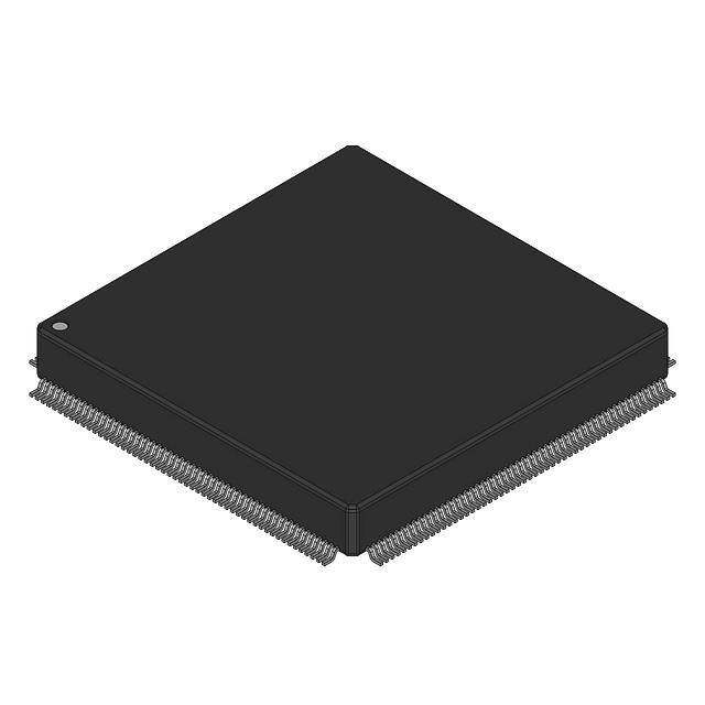
The ÉlanSC310 microcontroller is available in both 25and 33-MHz versions, in a 208-lead Plastic Shrink
Quad Flat Pack (QFP) (PQR package) and a 208-lead
Thin Quad Flat Pack (TQFP) (PQL package).
Note: Unless specified otherwise, the timings in this
data sheet are based on the 33-MHz version of the
ÉlanSC310 microcontroller.
CUSTOMER SERVICE
The AMD customer service network includes U.S. offices, international offices, and a customer training center. Expert technical assistance is available from the
AMD worldwide staff of field application engineers and
factory support staff who can answer E86 family hardware and software development questions.
Hotline and World Wide Web Support
For answers to technical questions, AMD provides a
toll-free number for direct access to our corporate applications hotline. Also available is the AMD World
Wide Web home page and FTP site, which provides the
latest E86 family product information.
Questions, requests, and input concerning AMD’s
WWW pages can be sent via E-mail to webmaster@amd.com.
To d own lo ad do cu me nt s a nd s oft war e , ft p t o
ftp.amd.com and log on as anonymous using your
e-mail address as a password. Or via your web
browser, go to ftp://ftp.amd.com.
Documentation and Literature
(800) 222-9323
Toll-free for U.S. and Canada
Free E86 family information such as data books, user’s
man ual s , data sh eets , ap pl ic ati on n otes , th e
FusionE86 Partner Solutions Catalog, and other literature is available with a simple phone call. Internationally, contact your local AMD sales office for complete
E86 family literature.
44-(0) 1276-803-299
U.K. and Europe hotline
Literature Ordering
Corporate Applications Hotline
World Wide Web Home Page and FTP Site
(800) 222-9323
Toll-free for U.S. and Canada
To ac c es s the AM D ho me pag e, g o to htt p:/ /
www.amd.com.
(512) 602-5651
Direct dial worldwide
2
Élan™SC310 Microcontroller Data Sheet
�P R E L I M I N A R Y
BLOCK DIAGRAM
SA11–SA0
IOR, IOW, MEMR,
MEMW, BALE
D15–D0
A20GATE, RC
MCS16, IOCS16,
IOCHRDY, 0WS
8042CS, SYSCLK
DACKx, TC, AEN
DREQx
DMA
Controller
(2x8237A-5)
Bus Controller
Local Bus
Controller
A23–A12, ADS, D/C,M/IO,
W/R, BHE, BLE, CPUCLK,
CPURST, CPURDY
LRDY, LDEV
Memory
Controller
RAS, CAS, MWE
PD15–PD0
Am386SXLV
PA23–PA0
M
U
X
CONTROL
Mapping
Registers
LFX
MA11/SA12–
MA0/SA23
PGP3–PGP0
X32IN
Clock
Generators
Power
Management
Control Unit
PMCx
ACIN, BLx, EXTSMI,
SUS/RES
Parallel Port
Control
PPDWE, PPOEN
AFDT, STRB, SLCTIN, INIT
ACK, BUSY, ERROR, PE, SLCT
X32OUT
Serial Port
(16450)
DTR, RTS, SOUT
CTS, DSR, DCD, SIN, RIN
Real-Time Clock
(146818A)
Programmable
Interval Timer
(8254)
Interrupt
Controller
(2x8259)
IRQx
Élan™SC310 Microcontroller Data Sheet
3
�P R E L I M I N A R Y
ORDERING INFORMATION
AMD standard products are available in several packages and operating ranges. The order numbers (Valid Combinations) are formed by a combination of the elements below.
ÉLANSC310
–25
K
C
TEMPERATURE RANGE
C = Commercial (0°C ≤ TAMBIENT ≤ 70°C)
I = Industrial (–40°C < TCASE ≤ 85°C)
PACKAGE TYPE
K = 208-lead QFP (Plastic Shrink Quad Flat Pack) (PQR-208)
V = 208-lead TQFP (Thin Quad Flat Pack) (PQL-208)
SPEED OPTION
–25 = 25 MHz
–33 = 33 MHz
DEVICE NUMBER/DESCRIPTION
ÉlanSC310 microcontroller highly integrated,
low-power, 32-bit microprocessor and system
logic
Valid Combinations
4
ELANSC310–25
KC
ELANSC310–33
KC
ELANSC310–25
KI
ELANSC310–33
KI
ELANSC310–25
VC
ELANSC310–33
VC
Valid Combinations
Valid Combinations list configurations planned to
be supported in volume for this device. Consult
the local AMD sales office to confirm availability
of specific valid combinations and to check on
newly released combinations.
Élan™SC310 Microcontroller Data Sheet
�P R E L I M I N A R Y
TABLE OF CONTENTS
Distinctive Characteristics ............................................................................................................ 1
General Description ..................................................................................................................... 2
Customer Service ........................................................................................................................ 2
Block Diagram ............................................................................................................................. 3
Ordering Information .................................................................................................................... 4
Connection Diagram .................................................................................................................. 11
ÉlanSC310 Microcontroller Pin Designations ............................................................................ 12
Pin Designations (Sorted by Pin Number) ................................................................................. 13
Pin Designations (Sorted By Pin Name) .................................................................................... 15
Pin State Tables ........................................................................................................................ 21
Pin Characteristics ................................................................................................................ 21
Pin Descriptions ......................................................................................................................... 30
Memory Bus Interface................................................................................................................ 30
CAS1H [SRCS3], CAS1L [SRCS2], CAS0H [SRCS1], CAS0L [SRCS0] ............................. 30
DOSCS ................................................................................................................................. 30
MA11–MA0/SA23–SA12....................................................................................................... 30
MWE ..................................................................................................................................... 30
RAS1–RAS0 ......................................................................................................................... 30
ROMCS................................................................................................................................. 30
System Interface ........................................................................................................................ 31
AEN [TDI] .............................................................................................................................. 31
D15–D0 ................................................................................................................................. 31
DACK2 [TCK] ........................................................................................................................ 31
DBUFOE ............................................................................................................................... 31
DRQ2 [TDO].......................................................................................................................... 31
ENDIRH ................................................................................................................................ 31
ENDIRL ................................................................................................................................. 31
IOCHRDY.............................................................................................................................. 31
IOCS16 ................................................................................................................................. 31
IOR........................................................................................................................................ 31
IOW ....................................................................................................................................... 31
IRQ1, IRQ14 ......................................................................................................................... 32
MCS16 .................................................................................................................................. 32
MEMR ................................................................................................................................... 32
MEMW .................................................................................................................................. 32
PIRQ0 (IRQ6), PIRQ1 (IRQ3) ............................................................................................... 32
RSTDRV ............................................................................................................................... 32
SA11–SA0............................................................................................................................. 32
SBHE .................................................................................................................................... 32
SPKR .................................................................................................................................... 32
TC [TMS]............................................................................................................................... 32
Keyboard Interface .................................................................................................................... 32
8042CS [XTDAT] .................................................................................................................. 32
A20GATE .............................................................................................................................. 32
RC ......................................................................................................................................... 33
SYSCLK [XTCLK] ................................................................................................................. 33
Parallel Port Interface ................................................................................................................ 33
ACK........................................................................................................................................ 33
AFDT [X14OUT].................................................................................................................... 33
BUSY .................................................................................................................................... 33
ERROR ................................................................................................................................. 33
INIT ....................................................................................................................................... 33
PE ......................................................................................................................................... 33
Élan™SC310 Microcontroller Data Sheet
5
�P R E L I M I N A R Y
PPDWE [PPDCS].................................................................................................................. 33
PPOEN.................................................................................................................................. 33
SLCT ..................................................................................................................................... 33
SLCTIN ................................................................................................................................. 33
STRB..................................................................................................................................... 33
Serial Port Interface ................................................................................................................... 33
CTS ....................................................................................................................................... 33
DCD ...................................................................................................................................... 33
DSR....................................................................................................................................... 33
DTR/CFG1 ............................................................................................................................ 34
RIN ........................................................................................................................................ 34
RTS/CFG0 ............................................................................................................................ 34
SIN ........................................................................................................................................ 34
SOUT .................................................................................................................................... 34
Power Management Interface .................................................................................................... 34
ACIN...................................................................................................................................... 34
BL4–BL1 ............................................................................................................................... 34
EXTSMI................................................................................................................................. 34
LPH ....................................................................................................................................... 34
PGP3–PGP0 ......................................................................................................................... 34
PMC4–PMC0 ........................................................................................................................ 34
SUS/RES .............................................................................................................................. 35
Miscellaneous Interface ............................................................................................................. 35
LF1, LF2, LF3, LF4 (Analog inputs) ...................................................................................... 35
X1OUT [BAUD-OUT] ............................................................................................................ 35
X14OUT ................................................................................................................................ 35
X32IN, X32OUT .................................................................................................................... 35
Local Bus Interface .................................................................................................................... 35
ADS....................................................................................................................................... 35
BHE....................................................................................................................................... 35
BLE ....................................................................................................................................... 35
CPUCLK (PULLUP) .............................................................................................................. 35
CPURDY ............................................................................................................................... 35
CPURST (RSVD) .................................................................................................................. 35
D/C ........................................................................................................................................ 35
LDEV (RSVD) ....................................................................................................................... 35
LRDY..................................................................................................................................... 36
M/IO ...................................................................................................................................... 36
W/R ....................................................................................................................................... 36
A23–A12 ............................................................................................................................... 36
Maximum ISA Bus Interface ...................................................................................................... 36
0WS ...................................................................................................................................... 36
BALE ..................................................................................................................................... 36
DACK7, DACK6, DACK5, DACK3, DACK2, DACK1, DACK0 .............................................. 36
DRQ7, DRQ6, DRQ5, DRQ3, DRQ2, DRQ1, DRQ0 ............................................................ 36
IOCHCHK.............................................................................................................................. 36
IRQ15, IRQ14, IRQ12–IRQ9, IRQ7–IRQ3, IRQ1 ................................................................. 36
LA23–LA17 ........................................................................................................................... 36
LMEG .................................................................................................................................... 36
JTAG Boundary Scan Interface ................................................................................................. 37
JTAGEN ................................................................................................................................ 37
[TCK] ..................................................................................................................................... 37
[TDI] ...................................................................................................................................... 37
[TDO]..................................................................................................................................... 37
[TMS]..................................................................................................................................... 37
6
Élan™SC310 Microcontroller Data Sheet
�P R E L I M I N A R Y
Reset and Power ....................................................................................................................... 37
AGND.................................................................................................................................... 37
AVCC .................................................................................................................................... 37
GND ...................................................................................................................................... 37
IORESET .............................................................................................................................. 37
RESIN ................................................................................................................................... 37
VCC....................................................................................................................................... 38
VCC1..................................................................................................................................... 38
VCC5..................................................................................................................................... 38
VMEM ................................................................................................................................... 38
VSYS..................................................................................................................................... 38
VSYS2................................................................................................................................... 38
Functional Description ............................................................................................................... 38
Am386SXLV CPU Core ........................................................................................................ 38
Memory Controller ................................................................................................................. 38
SRAM .................................................................................................................................... 41
The PMU Modes and Clock Generators ............................................................................... 41
ÉlanSC310 Microcontroller Power Management .................................................................. 44
Micro Power Off Mode .......................................................................................................... 46
Core Peripheral Controllers ................................................................................................... 50
Additional Peripheral Controllers ........................................................................................... 51
Parallel Port Anomalies ......................................................................................................... 53
PC/AT Support Features ....................................................................................................... 53
Local Bus or Maximum ISA Bus Controller ........................................................................... 56
Alternate Pin Functions .............................................................................................................. 59
Maximum ISA Interface versus Local Bus Interface ............................................................. 60
Alternate Pin Functions Selected Via Firmware ........................................................................ 61
SRAM Interface ..................................................................................................................... 61
Unidirectional/Bidirectional Parallel Port ............................................................................... 61
X1OUT [BAUD_OUT] Clock Source ..................................................................................... 61
PC/XT Keyboard ................................................................................................................... 62
14-MHz Clock Source ........................................................................................................... 62
ISA Bus Descriptions ................................................................................................................. 63
System Test and Debug ........................................................................................................ 64
JTAG Instruction Opcodes .................................................................................................... 69
Absolute Maximum Ratings ....................................................................................................... 70
Operating Ranges...................................................................................................................... 70
Thermal Characteristics ............................................................................................................. 72
Typical Power Numbers ............................................................................................................. 72
Derating Curves ......................................................................................................................... 73
Voltage Partitioning .................................................................................................................... 84
Crystal Specifications ................................................................................................................ 84
Loop Filters ................................................................................................................................ 86
AC Switching Characteristics and Waveforms .......................................................................... 87
AC Switching Test Waveforms .............................................................................................. 87
AC Switching Characteristics over Commercial Operating Ranges ...................................... 88
Physical Dimensions ................................................................................................................ 118
PQR 208, Trimmed and Formed Plastic Shrink Quad Flat Pack (QFP) ............................. 118
PQL 208, Trimmed and Formed Thin Quad Flat Pack (TQFP) ........................................... 119
Élan™SC310 Microcontroller Data Sheet
7
�P R E L I M I N A R Y
LIST OF FIGURES
Figure 1. PLL Block Diagram .................................................................................................. 42
Figure 2. Clock Steering Block Diagram ................................................................................. 43
Figure 3. Typical System Design with Secondary Power Supply to Maintain RTC When
Primary Power Supply is Off (DRAM Refresh is Optional.)...................................... 47
Figure 4. ÉlanSC310 Microcontroller I/O Structure ................................................................. 48
Figure 5. ÉlanSC310 Microcontroller Unidirectional Parallel Port Data Bus Implementation... 52
Figure 6. The ÉlanSC310 Microcontroller Bidirectional Parallel Port
and EPP Implementation ......................................................................................... 53
Figure 7. Typical System Block Diagram (Maximum ISA Mode)............................................. 55
Figure 8. Bus Option Configuration Select .............................................................................. 59
Figure 9. 3.3-V I/O Drive Type E Rise Time............................................................................ 74
Figure 10. 3.3-V I/O Drive Type E Fall Time ............................................................................. 74
Figure 11. 5-V I/O Drive Type E Rise Time............................................................................... 75
Figure 12. 5-V I/O Drive Type E Fall Time ................................................................................ 75
Figure 13. 3.3-V I/O Drive Type D Rise Time............................................................................ 76
Figure 14. 3.3-V I/O Drive Type D Fall Time ............................................................................. 76
Figure 15. 5-V I/O Drive Type D Rise Time............................................................................... 77
Figure 16. 5-V I/O Drive Type D Fall Time ................................................................................ 77
Figure 17. 3.3-V I/O Drive Type C Rise Time............................................................................ 78
Figure 18. 3.3-V I/O Drive Type C Fall Time ............................................................................. 78
Figure 19. 5-V I/O Drive Type C Rise Time............................................................................... 79
Figure 20. 5-V I/O Drive Type C Fall Time ................................................................................ 79
Figure 21. 3.3-V I/O Drive Type B Rise Time............................................................................ 80
Figure 22. 3.3-V I/O Drive Type B Fall Time ............................................................................. 80
Figure 23. 5-V I/O Drive Type B Rise Time............................................................................... 81
Figure 24. 5-V I/O Drive Type B Fall Time ................................................................................ 81
Figure 25. 3.3-V I/O Drive Type A Rise Time............................................................................ 82
Figure 26. 3.3-V I/O Drive Type A Fall Time ............................................................................. 82
Figure 27. 5-V I/O Drive Type A Rise Time............................................................................... 83
Figure 28. 5-V I/O Drive Type A Fall Time ................................................................................ 83
Figure 29. X32 Oscillator Circuit................................................................................................ 85
Figure 30. Loop-Filter Component ............................................................................................ 86
Figure 31. Key to Switching Waveforms ................................................................................... 87
Figure 32. Power-Up Sequence Timing .................................................................................... 89
Figure 33. Micro Power Off Mode Exit ...................................................................................... 90
Figure 34. Entering Micro Power Off Mode (DRAM Refresh Disabled) .................................... 91
Figure 35. Entering Micro Power Off Mode (DRAM Refresh Enabled) ..................................... 91
Figure 36. DRAM Timings, Page Hit ......................................................................................... 93
Figure 37. DRAM Timings, Refresh Cycle ................................................................................ 93
Figure 38. DRAM First Cycle and Bank/Page Miss (Read Cycles)........................................... 95
Figure 39. DRAM First Cycle Bank/Page Miss (Write Cycles) .................................................. 97
Figure 40. Local Bus Interface .................................................................................................. 99
Figure 41. BIOS ROM Read/Write 8-Bit Cycle........................................................................ 101
Figure 42. DOS ROM Read/Write 8-Bit Cycle......................................................................... 103
Figure 43. DOS ROM Read/Write 16-Bit Cycle....................................................................... 105
Figure 44. ISA Memory Read/Write 8-Bit Cycle ...................................................................... 107
Figure 45. ISA Memory Read/Write 16-Bit Cycle .................................................................... 109
Figure 46. ISA Memory Read/Write 0 Wait State Cycle.......................................................... 111
Figure 47. ISA I/O 8-Bit Read/Write Cycle .............................................................................. 113
Figure 48. ISA I/O 16-Bit Read/Write Cycle ............................................................................ 115
Figure 49. EPP Data Register Write Cycle.............................................................................. 116
Figure 50. EPP Data Register Read Cycle ............................................................................. 117
8
Élan™SC310 Microcontroller Data Sheet
�P R E L I M I N A R Y
LIST OF TABLES
Table 1.
Table 2.
Table 3.
Table 4.
Table 5.
Table 6.
Table 7.
Table 8.
Table 9.
Table 10.
Table 11.
Table 12.
Table 13.
Table 14.
Table 15.
Table 16.
Table 17.
Table 18.
Table 19.
Table 20.
Table 21.
Table 22.
Table 23.
Table 24.
Table 25.
Table 26.
Table 27.
Table 28.
Table 29.
Table 30.
Table 31.
Table 32.
Table 33.
Table 34.
Table 35.
Table 36.
Table 37.
Table 38.
Table 39.
Table 40.
Table 41.
Table 42.
Table 43.
Table 44.
Table 45.
Table 46.
Table 47.
Table 48.
Table 49.
Table 50.
I/O Pin Voltage Level ...............................................................................................
Memory Bus Interface ..............................................................................................
System Interface ......................................................................................................
Keyboard Interface...................................................................................................
Parallel Port Interface...............................................................................................
Serial Port Interface .................................................................................................
Power Management Interface ..................................................................................
Local Bus Interface ..................................................................................................
Miscellaneous Interface ...........................................................................................
Power Pins ...............................................................................................................
Non-Multiplexed Address Signals Provided by MA11–MA0 ....................................
DRAM Mode Selection.............................................................................................
MA and SA Signal Pin Sharing ................................................................................
Supported DRAM/SRAM Configuration ...................................................................
DRAM Address Translation (Page Mode)................................................................
DRAM Address Translation (Enhanced Page Mode)...............................................
SRAM Access Pins ..................................................................................................
SRAM Wait State Select Logic.................................................................................
High-Speed CPU Clock Frequencies.......................................................................
PLL Output ...............................................................................................................
PMU Modes .............................................................................................................
Internal Clock States ................................................................................................
Internal I/O Pulldown States.....................................................................................
Parallel Port EPP Mode Pin Definition .....................................................................
External Resistor Requirements ..............................................................................
Bus Option Select Bit Logic......................................................................................
Pins Shared Between Maximum ISA Bus and Local Bus Interface Functions.........
SRAM Interface........................................................................................................
Bidirectional Parallel Port Pin Description................................................................
X1OUT Clock Source Pin Description......................................................................
XT Keyboard Pin Description ...................................................................................
14-MHz Clock Source ..............................................................................................
ISA Bus Functionality ...............................................................................................
ISA Bus Functionality Lost when Configured for Local Bus Mode ...........................
Boundary Scan (JTAG) Cells—Order and Type ......................................................
ÉlanSC310 Microcontroller JTAG Instruction Opcodes ...........................................
DC Characteristics over Commercial and Industrial Operating Ranges
(Plastic Shrink Quad Flat Pack (QFP), 33 MHz, 3.3 V)............................................
DC Characteristics over Commercial and Industrial Operating Ranges
(Plastic Shrink Quad Flat Pack (QFP), 33 MHz, 5 V)...............................................
Commercial and Industrial Operating Voltage ranges at 25°C ................................
Thermal Resistance (°C/Watt) ψJT and θJA for 208-pin QFP and TQFP packages .
Typical Maximum ISA Mode Power Consumption ...................................................
I/O Drive Type Description (Worst Case).................................................................
Recommended Oscillator Component Value Limits.................................................
Loop-Filter Component Values ................................................................................
Power-Up Sequencing .............................................................................................
DRAM Memory Interface, Page Hit and Refresh Cycle ...........................................
DRAM First Cycle Read Access ..............................................................................
DRAM Bank/Page Miss Read Cycles ......................................................................
DRAM First Cycle Write Access...............................................................................
DRAM Bank/Page Miss Write Cycles ......................................................................
Élan™SC310 Microcontroller Data Sheet
21
22
23
24
25
25
26
26
28
29
30
39
39
39
40
40
41
41
44
44
45
45
50
52
56
59
60
61
61
61
62
62
63
63
65
69
70
71
71
72
72
73
85
86
88
92
94
94
96
96
9
�A D V A N C E
Table 51.
Table 52.
Table 53.
Table 54.
Table 55.
Table 56.
Table 57.
Table 58.
Table 59.
Table 60.
Table 61.
10
I N F O R M A T I O N
Local Bus Interface .................................................................................................. 98
BIOS ROM Read/Write 8-Bit Cycle........................................................................ 100
DOS ROM Read/Write 8-Bit Cycle......................................................................... 102
DOS ROM and Fast DOS ROM Read/Write 16-Bit Cycles.................................... 104
ISA Memory Read/Write 8-Bit Cycle ...................................................................... 106
ISA Memory Read/Write 16-Bit Cycle .................................................................... 108
ISA Memory Read/Write 0 Wait State Cycle ......................................................... 110
ISA I/O 8-Bit Read/Write Cycle .............................................................................. 112
ISA I/O 16-Bit Read/Write Cycle ............................................................................ 114
EPP Data Register Write Cycle.............................................................................. 116
EPP Data Register Read Cycle ............................................................................. 117
Élan™SC310 Microcontroller Data Sheet
�P R E L I M I N A R Y
208
207
206
205
204
203
202
201
200
199
198
197
196
195
194
193
192
191
190
189
188
187
186
185
184
183
182
181
180
179
178
177
176
175
174
173
172
171
170
169
168
167
166
165
164
163
162
161
160
159
158
157
AGND
LF4 Video PLL
LF3 Low Speed PLL
LF2 Internal PLL
LF1 High Speed PLL
AVCC
X32OUT
X32IN
X1OUT [BAUD OUT]
JTAGEN
IRQ14
MCS16
IOCS16
IRQ1
PIRQ0 (IRQ3)
PIRQ1 (IRQ6)
IOCHRDY
GND
LPH
PGP0
PGP1
PGP2
PGP3
PMC3
PMC4
PULLUP
IRQ15
IRQ12
VCC
PULLUP(IRQ10)
PULLDN(IRQ5)
IOCHCHK
VCC1
DRQ5
DRQ1
IRQ4
ADS(0WS)
D/C(DRQ0)
M/IO(DRQ3)
W/R(DRQ7)
BHE(IRQ9)
BLE(IRQ11)
LRDY(DRQ6)
RSVD(PULLUP)
PULLUP(IRQ7)
CPURST(RSVD)
CPUCLK(PULLUP)
A13(DACK6)
A14(DACK7)
A15(DACK3)
A16(DACK0)
GND
CONNECTION DIAGRAM
GND
RAS0
RAS1
CAS1L[SRCS2]
CAS1H[SRCS3]
CAS0L[SRCS0]
CAS0H[SRCS1]
MWE
VMEM
MA10/SA13
MA9/SA23
GND
MA8/SA22
MA7/SA21
MA6/SA20
MA5/SA19
MA4/SA18
MA3/SA17
MA2/SA16
GND
MA1/SA15
VMEM
VCC
MA0/SA14
D15
D14
D13
D12
D11
D10
D9
D8
GND
D7
VMEM
D6
D5
D4
D3
D2
D1
D0
DOSCS
ROMCS
SYSCLK[XTCLK]
DACK2 [TCK]
AEN [TDI]
VSYS
TC [TMS]
ENDIRL
ENDIRH
GND
GND
A17(LA17)
A18(LA18)
A19(LA19)
A20(LA20)
A21(LA21)
A22(LA22)
A23(LA23)
LDEV(RSVD)
CPURDY(LMEG)
DACK1
A12(BALE)
DACK5
SBHE
VSYS2
RESIN
IORESET
SPKR
PMC1
PMC0
RSVD
VCC
RSVD
RSVD
RSVD
RSVD
RSVD
RSVD
VCC5
RSVD
RSVD
RSVD
RSVD
RSVD
RSVD
GND
PULLUP
PULLUP
PULLUP
PULLUP
PULLUP
PULLUP
PULLUP
PULLUP
PULLUP
PULLUP
PULLUP
BL4
BL3
BL2
BL1
GND
156
155
154
153
152
151
150
149
148
147
146
145
144
143
142
141
140
139
138
137
136
135
134
133
132
131
130
129
128
127
126
125
124
123
122
121
120
119
118
117
116
115
114
113
112
111
110
109
108
107
106
105
GND
IOR
IOW
MEMR
MEMW
RSTDRV
DBUFOE
MA11/SA12
SA11
SA10
SA9
SA8
VSYS
SA7
SA6
GND
SA5
SA4
SA3
SA2
SA1
SA0
8042CS[XTDAT]
DRQ2 [TDO]
PMC2
RC
A20GATE
AFDT[X14OUT]
VCC
PE
STRB
SLCTIN
BUSY
ERROR
SLCT
ACK
INIT
PPWDE [PPDCS]
PPOEN
DTR/CFG1
RTS/CFG0
SOUT
VCC5
CTS
DSR
DCD
SIN
RIN
ACIN
EXTSMI
SUS/RES
GND
53
54
55
56
57
58
59
60
61
62
63
64
65
66
67
68
69
70
71
72
73
74
75
76
77
78
79
80
81
82
83
84
85
86
87
88
89
90
91
92
93
94
95
96
97
98
99
100
101
102
103
104
1
2
3
4
5
6
7
8
9
10
11
12
13
14
15
16
17
18
19
20
21
22
23
24
25
26
27
28
29
30
31
32
33
34
35
36
37
38
39
40
41
42
43
44
45
46
47
48
49
50
51
52
Notes:
Pin 1 is marked for designation purposes only.
Élan™SC310 Microcontroller Data Sheet
11
�P R E L I M I N A R Y
ÉLANSC310 MICROCONTROLLER PIN DESIGNATIONS
This section, beginning with the Connection Diagram
on the preceding page, identifies the pins of the
ÉlanSC310 microcontroller and lists the signals associated with each pin. Tables 2–10, beginning on page 22,
group these signals according to function. The table
beginning on page 13 lists the pins sorted by pin number; the table beginning on page 15 lists the pins sorted
by pin name along with the corresponding pin number,
functional grouping, Pin State table number, and the
page number where a description of the pin is located.
The Signal Name column in the pin designation table
(sorted by pin number), and in Tables 2–10, is decoded
as follows:
NAME1 / NAME2 [NAME3] (NAME4)
NAME1 - This is the pin function when the ÉlanSC310
microcontroller has been configured, at reset, for the
Local Bus mode of operation. If the pin only has one
function regardless of the mode, NAME1 is the only
name given.
NAME2 - This is the secondary pin function (by default)
when the ÉlanSC310 microcontroller has been configured, at reset, for the Local Bus mode of operation. If
the pin always has two functions regardless of the
mode, NAME1 followed by NAME2 are the only names
given.
NAME3 - This is a tertiary pin function that must be enabled specifically by firmware. As an example, for pins
DACK2[TCK], DRQ2[TDO], AEN[TDI], and TC[TMS],
the NAME3 function is selected by the JTAGEN pin
being asserted High (JTAG ENABLE).
NAME4 - Designates the pin function when the
ÉlanSC310 microcontroller has been configured, at reset, for the Maximum ISA mode of operation.
RSVD - Pins marked with this designator are required
to remain unconnected.
PULLUP - Needs external pull-up resistor.
PULLDN - Needs external pull-down resistor.
The Signal Name column in the pin designation table
(sorted by pin name), beginning on page 13, contains
an alphabetical listing of all pin names, followed by
their corresponding alternate pin names in the applicable format from those listed here:
NAME1 / NAME2 [NAME3] (NAME4 / NAME5)
NAME2 / NAME1 [NAME3] (NAME4 / NAME5)
[NAME3] (NAME4 / NAME5) NAME1 / NAME2
(NAME4 / NAME5) NAME1 / NAME2 [NAME3]
(NAME5 / NAME4) NAME1 / NAME2 [NAME3]
For more information about how pins are shared and
which functions are available in each bus mode, see
“Alternate Pin Functions” on page 59
12
Élan™SC310 Microcontroller Data Sheet
�P R E L I M I N A R Y
PIN DESIGNATIONS (SORTED BY PIN NUMBER)
Pin No.
Signal Name
(Alternate Functions)
Pin No.
Signal Name
(Alternate Functions)
Pin No.
Signal Name
(Alternate Functions)
1
GND
44
ROMCS
87
SLCT
2
RAS0
45
SYSCLK [XTCLK]
88
ACK
3
RAS1
46
DACK2 [TCK]
89
INIT
4
CAS1L [SRCS2]
47
AEN [TDI]
90
PPDWE [PPDCS]
5
CAS1H [SRCS3]
48
VSYS
91
PPOEN
6
CAS0L [SRCS0]
49
TC [TMS]
92
DTR/CFG1
7
CAS0H [SRCS1]
50
ENDIRL
93
RTS/CFG0
8
MWE
51
ENDIRH
94
SOUT
9
VMEM
52
GND
95
VCC5
10
MA10/SA13
53
GND
96
CTS
11
MA9/SA23
54
IOR
97
DSR
12
GND
55
IOW
98
DCD
13
MA8/SA22
56
MEMR
99
SIN
14
MA7/SA21
57
MEMW
100
RIN
15
MA6/SA20
58
RSTDRV
101
ACIN
16
MA5/SA19
59
DBUFOE
102
EXTSMI
17
MA4/SA18
60
MA11/SA12
103
SUS/RES
18
MA3/SA17
61
SA11
104
GND
19
MA2/SA16
62
SA10
105
GND
20
GND
63
SA9
106
BL1
21
MA1/SA15
64
SA8
107
BL2
22
VMEM
65
VSYS
108
BL3
23
VCC
66
SA7
109
BL4
24
MA0/SA14
67
SA6
110
PULLUP
25
D15
68
GND
111
PULLUP
26
D14
69
SA5
112
PULLUP
27
D13
70
SA4
113
PULLUP
28
D12
71
SA3
114
PULLUP
29
D11
72
SA2
115
PULLUP
30
D10
73
SA1
116
PULLUP
31
D9
74
SA0
117
PULLUP
32
D8
75
8042CS [XTDAT]
118
PULLUP
33
GND
76
DRQ2 [TDO]
119
PULLUP
34
D7
77
PMC2
120
PULLUP
35
VMEM
78
RC
121
GND
36
D6
79
A20GATE
122
RSVD
37
D5
80
AFDT [X14OUT]
123
RSVD
38
D4
81
VCC
124
RSVD
39
D3
82
PE
125
RSVD
40
D2
83
STRB
126
RSVD
41
D1
84
SLCTIN
127
RSVD
42
D0
85
BUSY
128
VCC5
43
DOSCS
86
ERROR
129
RSVD
Élan™SC310 Microcontroller Data Sheet
13
�P R E L I M I N A R Y
PIN DESIGNATIONS (SORTED BY PIN NUMBER) (CONTINUED)
Pin No.
14
Signal Name
(Alternate Functions)
Pin No.
Signal Name
(Alternate Functions)
Signal Name
(Alternate Functions)
Pin No.
130
RSVD
157
GND
184
PMC4
131
RSVD
158
A16 (DACK0)
185
PMC3
132
RSVD
159
A15 (DACK3)
186
PGP3
133
RSVD
160
A14 (DACK7)
187
PGP2
134
RSVD
161
A13 (DACK6)
188
PGP1
135
VCC
162
CPUCLK (PULLUP)
189
PGP0
136
RSVD
163
CPURST (RSVD)
190
LPH
137
PMC0
164
PULLUP (IRQ7)
191
GND
138
PMC1
165
RSVD (PULLUP)
192
IOCHRDY
139
SPKR
166
LRDY (DRQ6)
193
PIRQ1(IRQ6)
140
IORESET
167
BLE (IRQ11)
194
PIRQ0 (IRQ3)
141
RESIN
168
BHE (IRQ9)
195
IRQ1
142
VSYS2
169
W/R (DRQ7)
196
IOCS16
143
SBHE
170
M/IO (DRQ3)
197
MCS16
144
DACK5
171
D/C (DRQ0)
198
IRQ14
145
A12(BALE)
172
ADS (0WS)
199
JTAGEN
146
DACK1 (DACK1)
173
IRQ4
200
X1OUT [BAUD_OUT]
147
CPURDY (LMEG)
174
DRQ1
201
X32IN
148
LDEV (RSVD)
175
DRQ5
202
X32OUT
149
A23 (LA23)
176
VCC1
203
AVCC
150
A22 (LA22)
177
IOCHCHK
204
LF1
151
A21 (LA21)
178
PULLDN (IRQ5)
205
LF2
152
A20 (LA20)
179
PULLUP (IRQ10)
206
LF3
153
A19 (LA19)
180
VCC
207
LF4
154
A18 (LA18)
181
IRQ12
208
AGND
155
A17 (LA17)
182
IRQ15
-
-
156
GND
183
PULLUP
-
-
Élan™SC310 Microcontroller Data Sheet
�P R E L I M I N A R Y
PIN DESIGNATIONS (SORTED BY PIN NAME)
Signal Name
Pin No.
Function
Pin State
Table No.
Description
Page No.
(0WS) ADS
172
Maximum ISA bus interface
7
36
8042CS [XTDAT]
75
Keyboard interface
3
32
A12 (BALE)
145
Local bus interface
7
36
A13 (DACK6)
161
Local bus interface
7
36
A14 (DACK7)
160
Local bus interface
7
36
A15 (DACK3)
159
Local bus interface
7
36
A16 (DACK0)
158
Local bus interface
7
36
A17 (LA17)
155
Local bus interface
7
36
A18 (LA18)
154
Local bus interface
7
36
A19 (LA19)
153
Local bus interface
7
36
A20 (LA20)
152
Local bus interface
7
36
A20GATE
79
Keyboard interface
3
33
A21 (LA21)
151
Local bus interface
7
36
A22 (LA22)
150
Local bus interface
7
36
A23 (LA23)
149
Local bus interface
7
36
ACIN
101
Power management interface
6
34
ACK
88
Parallel port interface
4
33
ADS (0WS)
172
Local bus interface
7
35
AEN [TDI]
47
System interface
2
31
AFDT [X14OUT]
80
Parallel port interface
4
33
AGND
208
Power
9
37
AVCC
203
Power
9
37
(BALE) A12
145
Maximum ISA bus interface
7
36
[BAUD_OUT] X1OUT
200
Miscellaneous interface
8
35
BHE (IRQ9)
168
Local bus interface
7
35
BL1
106
Power management interface
6
34
BL2
107
Power management interface
6
34
BL3
108
Power management interface
6
34
BL4
109
Power management interface
6
34
BLE (IRQ11)
167
Local bus interface
7
35
BUSY
85
Parallel port interface
4
33
CAS0H [SRCS1]
7
Memory bus interface
1
30
CAS0L [SRCS0]
6
Memory bus interface
1
30
CAS1H [SRCS3]
5
Memory bus interface
1
30
CAS1L [SRCS2]
4
Memory bus interface
1
30
CFG0/RTS
93
Serial port interface
5
34
CFG/DTR
92
Serial port interface
5
34
CPUCLK (PULLUP)
162
Local bus interface
7
35
CPURDY (LMEG)
147
Local bus interface
7
35
CPURST (RSVD)
163
Local bus interface
7
35
CTS
96
Serial port interface
5
33
D/C (DRQ0)
171
Maximum ISA bus interface
7
35
D0
42
System interface
2
31
Élan™SC310 Microcontroller Data Sheet
15
�P R E L I M I N A R Y
PIN DESIGNATIONS (SORTED BY PIN NAME) (CONTINUED)
Signal Name
Pin No.
Function
Pin State
Table No.
Description
Page No.
D1
41
System interface
2
31
D10
30
System interface
2
31
D11
29
System interface
2
31
D12
28
System interface
2
31
D13
27
System interface
2
31
D14
26
System interface
2
31
D15
25
System interface
2
31
D2
40
System interface
2
31
D3
39
System interface
2
31
D4
38
System interface
2
31
D5
37
System interface
2
31
D6
36
System interface
2
31
D7
34
System interface
2
31
D8
32
System interface
2
31
D9
31
System interface
2
31
(DACK0) A16
158
Maximum ISA bus interface
7
36
DACK1 (DACK1)
146
Local and maximum ISA bus interface
2
36
DACK2 [TCK]
46
Local and maximum ISA bus interface
2
31, 36
(DACK3) A15
159
Maximum ISA bus interface
7
36
DACK5
144
Maximum ISA bus interface
2
36
(DACK6) A13
161
Maximum ISA bus interface
7
36
(DACK7) A14
160
Maximum ISA interface
7
36
DBUFOE
59
System interface
2
31
D/C (DRQ0)
171
Local bus interface
2
35
DCD
98
Serial port interface
5
33
DOSCS
43
Memory bus interface
1
30
(DRQ0) D/C
171
Maximum ISA bus interface
7
36
DRQ1
174
Local and Maximum ISA bus interface
2
36
DRQ2 [TDO]
76
Local and Maximum ISA interface
2
31, 36
(DRQ3) M/IO
170
Maximum ISA bus interface
7
36
DRQ5
175
Local and Maximum ISA bus interface
2
36
(DRQ6) LRDY
166
Maximum ISA bus interface
7
36
(DRQ7) W/R
169
Maximum ISA bus interface
DSR
97
Serial port interface
36
5
33
DTR/CFG1
92
Serial port interface
5
34
ENDIRH
51
System interface
2
31
ENDIRL
50
System interface
2
31
ERROR
86
Parallel port interface
4
33
EXTSMI
102
Power management interface
6
34
9
37
GND
16
1, 12, 20, Power
33, 52, 53,
68, 104,
105, 121,
156, 157,
191
Élan™SC310 Microcontroller Data Sheet
�P R E L I M I N A R Y
PIN DESIGNATIONS (SORTED BY PIN NAME) (CONTINUED)
Signal Name
Pin No.
Function
Pin State
Table No.
Description
Page No.
INIT
89
Parallel port interface
4
33
IOCHCHK
177
Maximum ISA bus interface
2
36
IOCHRDY
192
System interface
2
31
IOCS16
196
System interface
2
31
IOR
54
System interface
2
31
IORESET
140
Reset and power
8
37
IOW
55
System interface
2
31
IRQ1
195
System and maximum ISA bus interface
2
32, 36
(IRQ10) PULLUP
179
Maximum ISA bus interface
7
36
(IRQ11) BLE
167
Maximum ISA bus interface
7
36
IRQ12
181
System interface
2
36
IRQ14
198
System and maximum ISA bus interface
2
32, 36
IRQ15
182
System interface
2
36
(IRQ3) PIRQ0
194
System interface
2
36
IRQ4
173
System interface
2
36
(IRQ5) PULLDN
178
Maximum ISA bus interface
7
36
(IRQ6) PIRQ1
193
Maximum ISA bus interface
2
36
(IRQ7) PULLUP
164
Maximum ISA bus interface
7
36
(IRQ9) BHE
168
Maximum ISA bus interface
7
36
JTAGEN
199
JTAG boundary scan interface
8
37
(LA17) A17
155
Maximum ISA bus interface
7
36
(LA18) A18
154
Maximum ISA bus interface
7
36
(LA19) A19
153
Maximum ISA bus interface
7
36
(LA20) A20
152
Maximum ISA bus interface
7
36
(LA21) A21
151
Maximum ISA bus interface
7
36
(LA22) A22
150
Maximum ISA bus interface
7
36
(LA23) A23
149
Maximum ISA bus interface
7
36
LDEV (RSVD)
148
Local bus interface
7
35
LF1
204
Miscellaneous interface
8
35
LF2
205
Miscellaneous interface
8
35
LF3
206
Miscellaneous interface
8
35
LF4
207
Miscellaneous interface
8
35
(LMEG) CPURDY
147
Maximum ISA bus interface
7
36
LPH
190
Power management interface
6
34
LRDY (DRQ6)
166
Local bus interface
7
36
M/IO (DRQ3)
170
Local bus interface
7
36
MA0/SA14
24
Memory bus interface
1
30
MA1/SA15
21
Memory bus interface
1
30
MA10/SA13
10
Memory bus interface
1
30
MA11/SA12
60
Memory bus interface
1
30
MA2/SA16
19
Memory bus interface
1
30
MA3/SA17
18
Memory bus interface
1
30
MA4/SA18
17
Memory bus interface
1
30
MA5/SA19
16
Memory bus interface
1
30
Élan™SC310 Microcontroller Data Sheet
17
�P R E L I M I N A R Y
PIN DESIGNATIONS (SORTED BY PIN NAME) (CONTINUED)
Signal Name
Pin No.
Function
Pin State
Table No.
Description
Page No.
MA6/SA20
15
Memory bus interface
1
30
MA7/SA21
14
Memory bus interface
1
30
MA8/SA22
13
Memory bus interface
1
30
MA9/SA23
11
Memory bus interface
1
30
MCS16
197
System interface
2
32
MEMR
56
System interface
2
32
MEMW
57
System interface
2
32
MWE
8
Memory bus interface
1
30
PE
82
Parallel port interface
4
33
PGP0
189
Power management interface
6
34
PGP1
188
Power management interface
6
34
PGP2
187
Power management interface
6
34
PGP3
186
Power management interface
6
34
PIRQ0 (IRQ3)
194
System and maximum ISA bus interface
2
32, 36
PIRQ1 (IRQ6)
193
System and maximum ISA bus interface
2
32, 36
PMC0
137
Power management interface
6
34
PMC1
138
Power management interface
6
34
PMC2
77
Power management interface
6
34
PMC3
185
Power management interface
6
34
PMC4
184
Power management interface
6
34
PPDCS
90
Parallel port interface
4
33
PPDWE [PPDCS]
90
Parallel port interface
4
33
PPOEN
91
Parallel port interface
4
33
PULLDN (IRQ5)
178
Miscellaneous interface
8
12
110–120,
164, 179,
183
Miscellaneous interface
8
12
PULLUP
(PULLUP) CPUCLK
162
Local bus interface
7
12
(PULLUP) RSVD
165
Local bus interface
7
12
RAS0
2
Memory bus interface
1
30
RAS1
3
Memory bus interface
1
30
RC
78
Keyboard interface
3
33
RESIN
141
Reset and power
8
37
RIN
100
Serial port interface
5
34
ROMCS
44
Memory bus interface
1
30
RSTDRV
58
System interface
2
32
8
12
RSVD
122–127, Miscellaneous interface
129–134,
136
RSVD (PULLUP)
165
Miscellaneous interface
7
12
(RSVD) CPURST
163
Miscellaneous interface
7
35
(RSVD) LDEV
148
Miscellaneous interface
7
35
RTS/CFG0
93
Serial port interface
5
34
SA0
74
System interface
2
32
SA1
73
System interface
2
32
18
Élan™SC310 Microcontroller Data Sheet
�P R E L I M I N A R Y
PIN DESIGNATIONS (SORTED BY PIN NAME) (CONTINUED)
Signal Name
Pin No.
Function
Pin State
Table No.
Description
Page No.
SA10
62
System interface
2
32
SA11
61
System interface
2
32
SA12/MA11
60
System interface
2
30
SA13/MA10
10
System interface
2
30
SA14/MA0
24
System interface
2
30
SA15/MA1
21
System interface
2
30
SA16/MA2
19
System interface
2
30
SA17/MA3
18
System interface
2
30
SA18/MA4
17
System interface
2
30
SA19/MA5
16
System interface
2
30
SA2
72
System interface
2
32
SA20/MA6
15
System interface
2
30
SA21/MA7
14
System interface
2
30
SA22/MA8
13
System interface
2
30
SA23/MA9
11
System interface
2
30
SA3
71
System interface
2
32
SA4
70
System interface
2
32
SA5
69
System interface
2
32
SA6
67
System interface
2
32
SA7
66
System interface
2
32
SA8
64
System interface
2
32
SA9
63
System interface
2
32
SBHE
143
System interface
2
32
SIN
99
Serial port interface
5
34
SLCT
87
Parallel port interface
4
33
SLCTIN
84
Parallel port interface
4
33
SOUT
94
Serial port interface
5
34
SPKR
139
Miscellaneous interface
8
32
[SRCS0] CAS0L
6
Memory bus interface
1
30
[SRCS1] CAS0H
7
Memory bus interface
1
30
[SRCS2] CAS1L
4
Memory bus interface
1
30
[SRCS3] CAS1H
5
Memory bus interface
1
30
STRB
83
Parallel port interface
4
33
SUS/RES
103
Power management interface
6
35
SYSCLK [XTCLK]
45
System interface
2
32
TC [TMS]
49
System interface
2
32
[TCK] DACK2
46
JTAG boundary scan interface
2
37
[TDI] AEN
47
JTAG boundary scan interface
2
37
[TDO] DRQ2
76
JTAG boundary scan interface
2
37
[TMS] TC
49
JTAG boundary scan interface
2
37
VCC
23, 81,
135, 180
Power
9
38
VCC1
176
Power
9
38
VCC5
95, 128
Power
9
38
Élan™SC310 Microcontroller Data Sheet
19
�P R E L I M I N A R Y
PIN DESIGNATIONS (SORTED BY PIN NAME) (CONTINUED)
Signal Name
Pin No.
Function
Pin State
Table No.
Description
Page No.
VMEM
9, 22, 35
Power
9
38
VSYS
48, 65
Power
9
38
VSYS2
142
Power
9
38
W/R (DRQ7)
169
Local bus interface
7
36
[X14OUT] AFDT
80
Miscellaneous interface
8
35
X1OUT [BAUD_OUT]
200
Miscellaneous interface
8
35
X32IN
201
Miscellaneous interface
8
35
X32OUT
202
Miscellaneous interface
8
35
[XTCLK] SYSCLK
45
Keyboard interface
3
32
[XTDAT] 8042CS
75
Keyboard interface
3
32
20
Élan™SC310 Microcontroller Data Sheet
�P R E L I M I N A R Y
PIN STATE TABLES
The Pin State tables beginning on page 22 are grouped
by function based on their primary function when the
ÉlanSC310 microcontroller is configured at reset for
the internal LCD Controller mode (NAME1). The Pin
State tables also show the I/O type and reset state for
those pins that have been configured at reset for either
Local Bus mode or Maximum ISA Bus mode.
Pin Characteristics
The following information clarifies the meaning of the
Pin State tables beginning on page 22:
The letters in the I/O Type column of Tables 2–10 mean
the following:
I
O
– Input
– Output
STI – Schmitt Trigger Input
B
– Bidirectional
A
– Analog
The Term column refers to internal termination. The
letters in this column of Tables 2–10 mean the following:
PD – Pull-down resistor
PU – Pull-up resistor
The symbols (letters) in the Drive Type column specify
the drive capability of output pins. These specifications
can be found in the DC Characteristics section beginning on page 70 of this document. For a more complete
description of I/O Drive Types, see “Derating Curves”
on page 73 and Table 42 on page 73.
The Reset State column lists the I/O pin voltage level
when all of the VCC pins are stable and the RESIN
input is active. The level of the VCC pins correlating to
this data is shown in Table 1.
Table 1.
I/O Pin Voltage Level
Local
Bus (V)
Maximum
ISA (V)
VCC
3.3
3.3
AVCC
3.3
3.3
VCC5
5.0
5.0
VSYS2
3.3
5.0
VSYS
5.0
5.0
VMEM
3.3
3.3
VCC1
3.3
3.3
Pin Name
The VCCIO column refers to the voltage supply pin on
the ÉlanSC310 microcontroller that is directly connected to the output driver for the specified signal pin.
The VCC Clamp column refers to the voltage supply
pin on the ÉlanSC310 microcontroller that is directly
connected to the ESD protection diode (cathode) for
the specified signal pin. Any pin with a 5-V VCC Clamp
is a “5-V safe” input.
The Spec. Load (specification load) column is used to
determine derated AC timing. See of “Derating Curves”
on page 73 of this data sheet.
The Clock Off column describes the logic level of the
I/O pins while the ÉlanSC310 microcontroller is in any
of the power management modes where the CPU clock
is stopped, and power is still applied to both the VCCIO
and VCC clamp supply pins associated with that I/O
pin.
Élan™SC310 Microcontroller Data Sheet
21
�P R E L I M I N A R Y
Table 2. Memory Bus Interface
Pin
No.
I/O
Type
Drive
Type
Clock
Off
RAS01,3
2
O
E,D,C
RAS11,3
3
O
CAS1L [SRCS2]1,2
4
CAS1H [SRCS3]1,2
Signal Name
Term
Reset State
(volts)
VCCIO
VCC
Clamp
Spec.
Load
(pF)
Local
Bus
Max
ISA
Active
3.3/0
3.3/0
VMEM
VMEM
50
E,D,C
Active
3.3/0
3.3/0
VMEM
VMEM
50
O
D
Active
3.3/0
3.3/0
VMEM
VMEM
30
5
O
D
Active
3.3/0
3.3/0
VMEM
VMEM
30
CAS0L [SRCS0]1,2
6
O
D
Active
3.3/0
3.3/0
VMEM
VMEM
30
CAS0H [SRCS1]1,2
7
O
D
Active
3.3/0
3.3/0
VMEM
VMEM
30
MA10/SA133
10
O
E,D,C
0
3.3
3.3
VMEM
VMEM
70
MA9/SA233
11
O
E,D,C
0
3.3
3.3
VMEM
VMEM
70
MA8/SA223
13
O
E,D,C
0
3.3
3.3
VMEM
VMEM
70
MA7/SA213
14
O
E,D,C
0
3.3
3.3
VMEM
VMEM
70
MA6/SA203
15
O
E,D,C
0
3.3
3.3
VMEM
VMEM
70
MA5/SA193
16
O
E,D,C
0
3.3
3.3
VMEM
VMEM
70
MA4/SA183
17
O
E,D,C
0
3.3
3.3
VMEM
VMEM
70
MA3/SA173
18
O
E,D,C
0
3.3
3.3
VMEM
VMEM
70
MA2/SA163
19
O
E,D,C
0
3.3
3.3
VMEM
VMEM
70
MA1/SA153
21
O
E,D,C
0
3.3
3.3
VMEM
VMEM
70
MA0/SA143
24
O
E,D,C
0
3.3
3.3
VMEM
VMEM
70
MWE3
8
O
E,D,C
1
3.3
3.3
VMEM
VMEM
70
ROMCS
44
O
B
1
5.0
5.0
VSYS
VCC5
30
DOSCS
43
O
B
1
5.0
5.0
VSYS
VCC5
50
Notes:
1. These signals are active during reset.
2. These pins always default to their DRAM interface function.
3. The drive strength for these pins is programmable. E is the default.
All inputs that have VCC Clamp = 5 V are 5-V safe inputs regardless of their VCCIO.
22
Élan™SC310 Microcontroller Data Sheet
�P R E L I M I N A R Y
Table 3. System Interface
Pin No.
I/O
Type
MA11/SA12
60
O
E
SA11
61
O
SA10
62
SA9
Signal Name
Term
Drive
Type
Clock
Off
Reset State
(volts)
VCCIO
VCC
Clamp
Spec.
Load
(pF)
Local
Bus
Max
ISA
0
5.0
5.0
VSYS
VCC5
70
D
0
5.0
5.0
VSYS
VCC5
70
O
D
0
5.0
5.0
VSYS
VCC5
70
63
O
D
0
5.0
5.0
VSYS
VCC5
70
SA8
64
O
D
0
5.0
5.0
VSYS
VCC5
70
SA7
66
O
D
0
5.0
5.0
VSYS
VCC5
70
SA6
67
O
D
0
5.0
5.0
VSYS
VCC5
70
SA5
69
O
D
0
5.0
5.0
VSYS
VCC5
70
SA4
70
O
D
0
5.0
5.0
VSYS
VCC5
70
SA3
71
O
D
0
5.0
5.0
VSYS
VCC5
70
SA2
72
O
D
0
5.0
5.0
VSYS
VCC5
70
SA1
73
O
D
0
5.0
5.0
VSYS
VCC5
70
SA0
74
O
D
0
0.0
0.0
VSYS
VCC5
70
D152
25
B
PD
E,D,C
0
0.0
0.0
VMEM
VMEM
70
D142
26
B
PD
E,D,C
0
0.0
0.0
VMEM
VMEM
70
D132
27
B
PD
E,D,C
0
0.0
0.0
VMEM
VMEM
70
D122
28
B
PD
E,D,C
0
0.0
0.0
VMEM
VMEM
70
D112
29
B
PD
E,D,C
0
0.0
0.0
VMEM
VMEM
70
D102
30
B
PD
E,D,C
0
0.0
0.0
VMEM
VMEM
70
D92
31
B
PD
E,D,C
0
0.0
0.0
VMEM
VMEM
70
D82
32
B
PD
E,D,C
0
0.0
0.0
VMEM
VMEM
70
D72
34
B
PD
E,D,C
0
0.0
0.0
VMEM
VMEM
70
D62
36
B
PD
E,D,C
0
0.0
0.0
VMEM
VMEM
70
D52
37
B
PD
E,D,C
0
0.0
0.0
VMEM
VMEM
70
D42
38
B
PD
E,D,C
0
0.0
0.0
VMEM
VMEM
70
D32
39
B
PD
E,D,C
0
0.0
0.0
VMEM
VMEM
70
D22
40
B
PD
E,D,C
0
0.0
0.0
VMEM
VMEM
70
D12
41
B
PD
E,D,C
0
3.3
0.0
VMEM
VMEM
70
D02
42
B
PD
E,D,C
0
3.3
0.0
VMEM
VMEM
70
SYSCLK [XTCLK]1
45
O(STI)
—
B
0(–)
5.0/0
5.0/0
VSYS
VCC5
30
IRQ1
195
I
PU
—
—
4.4
4.4
VCC1
VCC5
—
PIRQ1 (IRQ6)
193
I
PU
–(–)
–(–)
3.3
3.3
VCC1
VCC5
—
PIRQ0 (IRQ3)
194
I
PU
–(–)
–(–)
3.3
3.3
VCC1
VCC5
—
DACK2 [TCK]
46
O(I)
—
B
1
5.0
5.0
VSYS
VCC5
30
DRQ2 [TDO]
76
I(O)
PD
A
—
0.0
0.0
VSYS
VCC5
30
AEN [TDI]
47
O(I)
—
B
1
0.0
0.0
VSYS
VCC5
30
Élan™SC310 Microcontroller Data Sheet
23
�P R E L I M I N A R Y
Table 3.
Pin No.
I/O
Type
TC [TMS]
49
ENDIRL
ENDIRH
System Interface (Continued)
Term
Drive
Type
Clock
Off
O(I)
—
B
50
O
—
51
O
—
DBUFOE
59
O
IOR
54
IOW
MEMR
Signal Name
Reset State
(volts)
VCCIO
VCC
Clamp
Spec.
Load
(pF)
Local
Bus
Max
ISA
0
0.0
0.0
VSYS
VCC5
30
B
1
5.0
5.0
VSYS
VCC5
30
B
1
5.0
5.0
VSYS
VCC5
30
—
B
1
5.0
5.0
VSYS
VCC5
30
O
—
C
1
5.0
5.0
VSYS
VCC5
50
55
O
—
C
1
5.0
5.0
VSYS
VCC5
50
56
O
—
C
1
5.0
5.0
VSYS
VCC5
50
MEMW
57
O
—
C
1
5.0
5.0
VSYS
VCC5
50
RSTDRV
58
O
—
A
0
5.0
5.0
VSYS
VCC5
30
IOCHRDY
192
STI
PU
—
—
3.3
3.3
VCC1
VCC5
—
DACK1
146
O
—
B
1
3.3
5.0
VSYS2
VCC5
30
DRQ1
174
I
—
C
—
0.0
0.0
VCC1
VCC5
100
DACK5
144
O
—
C
1
3.3
5.0
VSYS2
VCC5
100
DRQ5
175
I
—
C
—
3.3
0.0
VCC1
VCC5
100
IOCHCHK
177
I
—
C
—
3.3
3.3
VCC1
VCC5
100
IRQ4
173
I
—
C
—
3.3
3.3
VCC1
VCC5
100
IRQ12
181
I
—
C
—
3.3
3.3
VCC1
VCC5
100
IRQ15
182
I
—
B
—
3.3
3.3
VCC1
VCC5
50
IOCS16
196
I
—
C
—
3.3
3.3
VCC1
VCC5
70
MCS16
197
I
—
C
—
3.3
3.3
VCC1
VCC5
70
IRQ14
198
I
—
C
—
0.0
0.0
VCC1
VCC5
70
SBHE
143
O
—
C
0
0.0
0.0
VSYS2
VCC5
70
VCCIO
VCC
Clamp
Spec.
Load
(pF)
VSYS
VCC5
30
Notes:
1. Reset State SYSCLK frequency is 4.6 MHz.
2. The drive strength for these pins is programmable. E is the default.
All inputs that have VCC clamp = 5 V are 5-V safe inputs regardless of their VCCIO.
Table 4. Keyboard Interface
Signal Name
8042CS [XTDAT]
Pin No.
I/O
Type
75
O(STI)
Term
Drive
Type
Clock
Off
—
B
1(–)
Reset State
(volts)
Local
Bus
Max
ISA
5.0
5.0
RC
78
I
PU
—
—
5.0
5.0
VSYS
VCC5
—
A20GATE
79
I
PU
—
—
5.0
5.0
VSYS
VCC5
—
Notes:
All inputs that have VCC clamp = 5 V are 5-V safe inputs regardless of their VCCIO.
24
Élan™SC310 Microcontroller Data Sheet
�P R E L I M I N A R Y
Table 5. Parallel Port Interface
Pin No.
I/O
Type
Term
Drive
Type
Clock
Off
AFDT [X14OUT]1
80
O
—
D
INIT1
89
O
—
STRB1
83
O
SLCTIN1
84
ACK
BUSY2
Signal Name
Reset State
(volts)
VCCIO
VCC
Clamp
Spec.
Load
(pF)
Local
Bus
Max
ISA
Last
state
5.0
5.0
VCC5
VCC5
100
D
Last
state
0.0
0.0
VCC5
VCC5
100
—
D
Last
state
5.0
5.0
VCC5
VCC5
100
O
—
D
Last
state
5.0
5.0
VCC5
VCC5
100
88
I
—
—
—
5.0
5.0
VCC5
VCC5
—
85
I
—
—
—
5.0
5.0
VCC5
VCC5
—
ERROR
86
I
—
—
—
5.0
5.0
VCC5
VCC5
—
PE
82
I
—
—
—
5.0
5.0
VCC5
VCC5
—
SLCT
87
I
—
—
—
5.0
5.0
VCC5
VCC5
—
PPDWE [PPDCS]
90
O
—
B
1(1)
5.0
5.0
VCC5
VCC5
30
PPOEN
91
O
—
B
1(1)
0.0
0.0
VCC5
VCC5
30
Notes:
1. These outputs function as open-drain outputs in Normal Parallel Port mode, and function as CMOS drivers when the EPPMODE configuration bit is set.
2. The parallel port interface BUSY input must have an external pullup if the parallel port is to be used in EPP mode. If this pullup
is not present, accesses to the parallel port in EPP mode will lock up the system.
All inputs that have VCC clamp = 5 V are 5-V safe inputs regardless of their VCCIO.
Table 6.
Pin No.
I/O
Type
DTR/CFG11
92
RTS/CFG01
Serial Port Interface
Term
Drive
Type
Clock
Off
O
—
A
93
O
—
SOUT
94
O
CTS
96
DCD
98
DSR
Signal Name
Reset State
(volts)
VCCIO
VCC
Clamp
Spec.
Load
(pF)
Local
Bus
Max
ISA
Last state
5.0
0
VCC5
VCC5
50
A
Last state
0.0
5.0
VCC5
VCC5
50
—
A
Last state
0.0
5.0
VCC5
VCC5
50
I
PU
—
—
5.0
5.0
VCC5
VCC5
—
I
PU
—
—
5.0
5.0
VCC5
VCC5
—
97
I
PU
—
—
5.0
5.0
VCC5
VCC5
—
RIN
100
I
PU
—
—
5.0
5.0
VCC5
VCC5
—
SIN
99
I
PU
—
—
5.0
5.0
VCC5
VCC5
—
Notes:
1. These pins are terminated externally per bus option selection.
All inputs that have VCC clamp = 5 V are 5-V safe inputs regardless of their VCCIO.
Élan™SC310 Microcontroller Data Sheet
25
�P R E L I M I N A R Y
Table 7. Power Management Interface
Pin No.
I/O
Type
Term
Drive
Type
Clock
Off
ACIN
101
STI
PD
—
EXTSMI
102
STI
PD
SUS/RES
103
STI
PMC41
184
PMC31
Signal Name
Reset State
(volts)
VCCIO
VCC
Clamp
Spec.
Load
(pF)
Local
Bus
Max
ISA
—
0.0
0.0
VCC5
VCC5
—
—
—
0.0
0.0
VCC5
VCC5
—
—
—
—
5.0
5.0
VCC5
VCC5
—
O
—
B
Active
0.0
0.0
VCC1
VCC5
50
185
O
—
B
Active
3.3
3.3
VCC1
VCC5
50
PMC21
77
O
—
B
Active
0.0
0.0
VSYS
VCC5
50
PMC11
138
O
—
B
Active
0.0
0.0
VCC5
VCC5
50
PMC01
137
O
—
B
Active
0.0
0.0
VCC5
VCC5
50
PGP3
186
O
—
B
Active
3.3
3.3
VCC1
VCC5
50
PGP2
187
O
—
B
Active
3.3
3.3
VCC1
VCC5
50
PGP1
188
B
—
B
Active
3.3
3.3
VCC1
VCC5
50
PGP0
189
B
—
B
Active
0.0
0.0
VCC1
VCC5
50
BL1
106
STI
—
—
—
5.0
5.0
VCC5
VCC5
—
BL2
107
STI
—
—
—
5.0
5.0
VCC5
VCC5
—
BL3
108
STI
—
—
—
5.0
5.0
VCC5
VCC5
—
BL4
109
STI
—
—
—
5.0
5.0
VCC5
VCC5
—
LPH
190
O
—
B
Active
0.0
0.0
VCC1
VCC5
50
Notes:
1. PMC outputs: four Low (PMC0, PMC1, PMC2, PMC4), one High (PMC3), default state after reset. All five are programmable
as either active High or Low after reset.
All inputs that have VCC clamp = 5 V are 5-V safe inputs regardless of their VCCIO.
Table 8. Local Bus Interface
Signal Name
ADS (0WS)
Pin No.
I/O
Type
Term
Drive
Type
Clock
Off
Reset State
(volts)
Local
Bus
Max
ISA
VCCIO
VCC
Clamp
Spec.
Load
(pF)
172
(O/I)
—
C
(1/–)
3.3
3.3
VCC1
VCC5
50
171
(O/I)
—
C
(LS/–)
3.3
0.0
VCC1
VCC5
50
M/IO (DRQ3)1
170
(O/I)
—
C
(LS/–)
0.0
0.0
VCC1
VCC5
50
W/R (DRQ7)1
169
(O/I)
—
C
(LS/–)
0.0
0.0
VCC1
VCC5
50
BHE (IRQ9)1
168
(O/I)
—
C
(LS/–)
0.0
3.3
VCC1
VCC5
50
BLE (IRQ11)1
167
(O/I)
—
C
(LS/–)
0.0
3.3
VCC1
VCC5
50
LRDY (DRQ6)
166
(I/I)
—
C
—
0.0
0.0
VCC1
VCC5
50
LDEV (RSVD)
148
(I/O)
—
C
(–/3 state)
3.3
0.0
VSYS2
VCC5
50
A23 (LA23)
149
O
—
C
0
3.3
5.0
VSYS2
VCC5
50
A22 (LA22)
150
O
—
C
0
3.3
5.0
VSYS2
VCC5
50
A21 (LA21)
151
O
—
C
0
3.3
5.0
VSYS2
VCC5
50
D/C
26
(DRQ0)1
Élan™SC310 Microcontroller Data Sheet
�P R E L I M I N A R Y
Table 8. Local Bus Interface (Continued)
Pin No.
I/O
Type
Term
Drive
Type
Clock
Off
A20 (LA20)
152
O
—
C
A19 (LA19)
153
O
—
A18 (LA18)
154
O
A17 (LA17)
155
A16 (DACK0)
158
A15 (DACK3)
Signal Name
Reset State
(volts)
VCCIO
VCC
Clamp
Spec.
Load
(pF)
Local
Bus
Max
ISA
0
3.3
5.0
VSYS2
VCC5
50
C
0
3.3
5.0
VSYS2
VCC5
50
—
C
0
3.3
5.0
VSYS2
VCC5
50
O
—
C
0
3.3
5.0
VSYS2
VCC5
50
O
—
C
(0/1)
3.3
5.0
VSYS2
VCC5
50
159
O
—
C
(0/1)
3.3
5.0
VSYS2
VCC5
50
A14 (DACK7)
160
O
—
C
(0/1)
3.3
5.0
VSYS2
VCC5
50
A13 (DACK6)
161
O
—
C
(0/1)
3.3
5.0
VSYS2
VCC5
50
162
O
—
E
0
3.3/0
3.3
VCC1
VCC5
50
(30)
CPURST (RSVD)
163
O
—
C
0
3.3
0.0
VCC1
VCC5
50
PULLUP (IRQ7)
164
I
—
C
—
3.3
3.3
VCC1
VCC5
50
RSVD (PULLUP)
165
(0/I)
—
C
(0/–)
3.3
3.3
VCC1
VCC5
50
PULLUP
183
I
—
B
—
3.3
3.3
VCC1
VCC5
30
CPUCLK
(PULLUP)2
CPURDY (LMEG)
147
O
—
B
1
0.0
0.0
VSYS2
VCC5
50
PULLDN (IRQ5)
178
I
—
C
—
0.0
3.3
VCC1
VCC5
100
PULLUP (IRQ10)
179
I
—
C
—
0.0
3.3
VCC1
VCC5
100
A12 (BALE)
145
O
—
E
(0/1)
3.3
5.0
VSYS2
VCC5
50
Notes:
1. LS in the Clock Off column stands for Last State.
2. Reset State Local Bus signal loading 920 mV–0 V. For 33-MHz operation, CPUCLK loading = 30 pF.
All inputs that have VCC clamp = 5 V are 5-V safe inputs regardless of their VCCIO.
Élan™SC310 Microcontroller Data Sheet
27
�P R E L I M I N A R Y
Table 9.
Miscellaneous Interface
Pin No.
I/O
Type
Term
Drive
Type
Clock
Off
IORESET1
140
I
—
—
X32IN2
201
I
—
X32OUT3
202
O
LF1
204
LF2
Signal Name
Reset State
(volts)
VCCIO
VCC
Clamp
Spec.
Load
(pF)
Local
Bus
Max
ISA
—
0.0
0.0
VCC5
VCC5
—
—
—
920/0
920/0
AVCC
AVCC
—
—
osc.
Active
1.68/0
1.68/0
AVCC
AVCC
—
A
—
—
—
1.52
1.52
AVCC
AVCC
—
205
A
—
—
—
1.48
1.48
AVCC
AVCC
—
LF3
206
A
—
—
—
1.52
1.52
AVCC
AVCC
—
LF4
207
A
—
—
—
1.68
1.68
AVCC
AVCC
—
X1OUT [BAUD_OUT]
200
O
—
B
(LS)
1.24
1.24
VCC1
VCC5
50
RESIN
141
STI
—
—
—
0.0
0.0
VCC
VCC
—
SPKR4
139
O
—
B
(LS)
5.0
5.0
VCC5
VCC5
50
JTAGEN
199
I
PD
—
—
0.0
0.0
VCC1
VCC5
—
RSVD
129
—
—
—
—
—
—
VCC5
VCC5
—
RSVD
130
—
—
—
—
—
—
VCC5
VCC5
—
RSVD
131
—
—
—
—
—
—
VCC5
VCC5
—
RSVD
132
—
—
—
—
—
—
VCC5
VCC5
—
(4)
(4)
RSVD
133
—
—
—
—
—
—
VCC5
VCC5
—
PULLUP
110
—
—
—
—
—
—
VCC5
VCC5
—
PULLUP
111
—
—
—
—
—
—
VCC5
VCC5
—
PULLUP
112
—
—
—
—
—
—
VCC5
VCC5
—
PULLUP
113
—
—
—
—
—
—
VCC5
VCC5
—
PULLUP
114
—
—
—
—
—
—
VCC5
VCC5
—
PULLUP
115
—
—
—
—
—
—
VCC5
VCC5
—
RSVD
122
—
—
—
—
—
—
VCC5
VCC5
—
RSVD
123
—
—
—
—
—
—
VCC5
VCC5
—
RSVD
124
—
—
—
—
—
—
VCC5
VCC5
—
RSVD
125
—
—
—
—
—
—
VCC5
VCC5
—
RSVD
126
—
—
—
—
—
—
VCC5
VCC5
—
RSVD
127
—
—
—
—
—
—
VCC5
VCC5
—
PULLUP
116
—
—
—
—
—
—
VCC5
VCC5
—
PULLUP
117
—
—
—
—
—
—
VCC5
VCC5
—
PULLUP
118
—
—
—
—
—
—
VCC5
VCC5
—
PULLUP
119
—
—
—
—
—
—
VCC5
VCC5
—
PULLUP
120
—
—
—
—
—
—
VCC5
VCC5
—
RSVD
134
—
—
—
—
—
—
VCC5
VCC5
—
RSVD
136
—
—
—
—
—
—
VCC5
VCC5
—
Notes:
1. IORESET (pin #140) requires an external pulldown resistor (~100K).
2. Reset State Local Bus signal and Reset State ISA Max signal: 920 mV–0 V frequency = 32 kHz.
3. Reset State signal: 1.68 V–0 V frequency = 32 kHz.
4. LS in the Clock Off column stands for Last State.
28
Élan™SC310 Microcontroller Data Sheet
�P R E L I M I N A R Y
All inputs that have VCC clamp = 5 V are 5-V safe inputs regardless of their VCCIO.
Table 10. Power Pins
Signal Name
Pin No.
I/O
Type
Term
Drive Clock
Type
Off
Reset State
(volts)
Local
Bus
Max
ISA
VCCIO
VCC
Clamp
Spec.
Load
(pF)
AVCC1
203
—
—
—
—
3.3
3.3
—
—
—
VCC1
23, 81, 135,180
—
—
—
—
3.3
3.3
—
—
—
VCC51
95, 128
—
—
—
—
5.0
5.0
—
—
—
VSYS21
142
—
—
—
—
3.3
5.0
—
—
—
VSYS1
48, 65
—
—
—
—
5.0
5.0
—
—
—
VMEM1
9, 22, 35
—
—
—
—
3.3
3.3
—
—
—
VCC11
176
—
—
—
—
3.3
3.3
—
—
—
GND
1,12, 20, 33, 52,
53, 68, 104, 105,
121, 156, 157,
191
—
—
—
—
—
—
—
—
—
AGND
208
—
—
—
—
—
—
—
—
—
Notes:
1. These reset state entries identify the VCCIO levels that are present on the ÉlanSC310 microcontroller for the two bus mode
options. Note that the device is not limited to these VCC levels.
All inputs that have VCC clamp = 5 V are 5-V safe inputs regardless of their VCCIO.
Élan™SC310 Microcontroller Data Sheet
29
�P R E L I M I N A R Y
PIN DESCRIPTIONS
Descriptions of the ÉlanSC310 microcontroller pins are
organized into the following functional groupings:
n Power management interface
n Memory bus interface
n Local bus interface
n System interface
n Maximum ISA bus interface
n Keyboard interface
n JTAG-boundary scan interface
n Parallel port interface
n Reset and power
n Miscellaneous interface
n Serial port interface
MEMORY BUS INTERFACE
CAS1H [SRCS3], CAS1L [SRCS2],
CAS0H [SRCS1], CAS0L [SRCS0]
as shown in Table 11. See also SA11–SA0 on
page 32.
Column Address Strobe (Outputs; Active Low)
Column Address Strobe indicates to DRAM that a valid
column address is present on the MA10–MA0 lines.
Two CAS signals are allocated to each 16-bit bank, one
per byte.
When SRAM, instead of DRAM, is configured as main
memory, SRCS3, SRCS2, SRCS1, and SRCS0 are the
alternate pin functions corresponding to CAS1H,
CAS1L, CAS0H, and CAS0L respectively. Each pin selects a byte in one of two possible 16 bit wide SRAM
banks. The SRAM functionality is selected via firmware. In this mode, all four of these outputs are active
Low. For more information about SRCS3–SRCS0, see
page 41.
DOSCS
DOS ROM Chip Select (Output; Active Low)
The DOS ROM Chip Select is an active Low output that
provides the chip select function for the Flash/ROM
array banks that are used to hold the operating system
or application code. DOSCS is used to select the DOS
ROMs and can be configured to respond to direct addressing or Memory Management System (MMS) addressing.
MA11–MA0/SA23–SA12
Memory Address (Outputs; Active High)
Memory address lines for multiplexed and nonmultiplexed memory devices; their effect depends on the
system configuration and the type of bus cycle.
n When the system is configured as DRAM, the
MA10–MA0 signals are multiplexed outputs and
convey the row address during RAS assertion and
column address during CAS assertion.
Table 11. Non-Multiplexed Address Signals
Provided by MA11–MA0
MA 11 10
SA
9
8
7
6
5
4
3
2
1
0
12 13 23 22 21 20 19 18 17 16 15 14
MWE
Write Enable (Output; Active Low)
Write Enable is the write command strobe for the
DRAM and SRAM devices.
RAS1–RAS0
Row Address Strobe (Output; Active Low)
Row Address Strobe indicates to DRAM that a valid
row address is present on the MA11–MA0 lines. One
RAS signal is allocated for each DRAM bank, one per
word.
ROMCS
BIOS ROM Chip Select (Output; Active Low)
BIOS ROM Chip Select is an active Low output that
provides the chip select function for the Flash/ROM array. ROMCS is used to select the BIOS ROM, and can
be configured to respond to direct addressing or MMS
addressing. When configured for direct addressing, the
BIOS ROM can reside at one or all of the following address ranges:
0F0000h–0FFFFFh
0E0000h–0EFFFFh
0D0000h–0DFFFFh
0C0000h–0CFFFFh
0A0000h–0AFFFFh
n When system memory is configured as SRAM,
MA11–MA0 output the system addresses, SA12–
SA23, and are used in conjunction with SA1–SA11.
The BIOS ROM chip select is also active for accesses
into the 64K segment that contains the boot vector, at
address FF0000h to FFFFFFh.
n For cycles that are not targeted to system memory
or internal I/O, MA11–MA0 are used to provide nonmultiplexed ISA-type address signals SA23–SA12,
For more information about the ROMCS pin, see the
Using 16-Bit ROMCS Designs in ÉlanTM SC300 and
ÉlanSC310 Microcontrollers Application Note, order
#21825.
30
Élan™SC310 Microcontroller Data Sheet
�P R E L I M I N A R Y
SYSTEM INTERFACE
ENDIRH
AEN [TDI]
High Byte Data Buffer Direction Control
(Output; Active High)
DMA Address Enable (Output; Active High)
AEN is used to indicate that the current address active
on the SA23–SA0 address bus is a memory address
and that the current cycle is a DMA cycle. All I/O devices should use this signal in decoding their I/O addresses and should not respond when this signal is
asserted. When AEN is asserted, the DACKx signals
are used to select the appropriate I/O device for the
DMA transfer.
This output controls the transceiver on the high byte of
the data bus, bits 15–8. When asserted, this signal is
used to enable the data from the ÉlanSC310 microcontroller data bus to the buffered data bus.
ENDIRL
Low Byte Data Buffer Direction Control
(Output; Active High)
This is a dual-function pin. When the JTAGEN signal is
asserted, it functions as the TDI, JTAG Test Data Input
pin.
This output controls the transceiver on the low byte of
the data bus, bits 7–0. When asserted, this signal is
used to enable the data from the ÉlanSC310 microcontroller data bus to the buffered data bus.
D15–D0
IOCHRDY
System Data Bus (Bidirectional; Active High)
I/O Channel Ready (Input; Active High)
The System Data Bus inputs data during memory and
I/O read cycles, and outputs data during memory and
I/O write cycles. During Local Bus and DRAM/SRAM
cycles, this bus represents the CPU data bus.
This signal is used by ISA slave devices to add wait
states to the current transfer. When this signal is deasserted, wait states are added.
DACK2 [TCK]
(Input; Active Low)
DMA Channel 2 Acknowledge (Output; Active Low)
This input is used to signal to the ISA control logic that
the targeted I/O device is a 16-bit device.
This output indicates that the current transfer is a DMA
transfer to the I/O device connected to this DMA channel. In PC-compatible system designs, this signal can
be connected to the floppy disk controller DMA acknowledge input.
This is a dual-function pin. When the JTAGEN signal is
asserted, it functions as the TCK (JTAG Test Clock)
pin. See “JTAG Boundary Scan Interface” on page 37
for more information on the function of this pin during
Test mode.
DBUFOE
Data Buffer Output Enable (Output; Active Low)
This output is used to control the output enable on the
system data bus buffer. When Low, the outputs of the
Data Bus Buffer are enabled.
DRQ2 [TDO]
DMA Channel 2 Request (Input; Active High
with Internal Pulldown)
This input is used to request a DMA transfer. It can be
connected to the floppy disk controller DMA request
output in PC-compatible system designs.
This is a dual-function pin. When the JTAGEN signal is
asserted, it will function as the TDO, JTAG Test Data
Out pin. See the “JTAG Boundary Scan Interface” on
page 37 for more information on the function of this pin
during Test mode.
IOCS16
IOCS16 is generated by a 16-bit ISA I/O expansion
board when the board recognizes it is being addressed. IOCS16 provides the same function for 16-bit
I/O expansion devices as the MCS16 signal provides for
16-bit memory devices.
Note: IOCS16 is internally ORed with MCS16. Do not
tie IOCS16 Low.
For more information about the IOCS16 pin, see the
Using 16-Bit ROMCS Designs in ÉlanTM SC300 and
ÉlanSC310 Microcontrollers Application Note, order
#21825.
IOR
I/O Read Command (Output; Active Low)
The IOR signal indicates that the current cycle is a read
of the currently selected I/O device. When this signal is
asserted, the selected I/O device can drive data onto
the data bus.
IOW
I/O Write Command (Output; Active Low)
The IOW signal indicates that the current cycle is a
write of the currently selected I/O device. When this
signal is asserted, the selected I/O device can latch
data from the data bus.
Élan™SC310 Microcontroller Data Sheet
31
�P R E L I M I N A R Y
IRQ1, IRQ14
RSTDRV
Interrupt Request Channels 1 and 14 (Input; Rising
Edge/Active High, with Internal Pullup)
System Reset (Output; Active High)
This input is connected to the internal 8259A-compatible Interrupt Controller Channels 1 and 14. In PC-compatible systems, IRQ1 may be connected to the 8042
keyboard controller.
MCS16
This signal is the ISA-compatible reset signal. When
this signal is asserted, all connected devices reinitialize
to their reset state. The pulse width of RSTDRV is adjustable based on PLL startup timings. For more information, see “Loop Filters” on page 86 and the powerup sequence timings beginning on page 88.
(Input; Active Low)
SA11–SA0
This input is used to signal to the ISA control logic that
the targeted memory device is a 16-bit device.
System Address Bus (Output; Active High)
MCS16 is generated by a 16-bit memory expansion
card when the card recognizes it is being addressed.
This signal tells the data bus steering logic that the addressed memory device is capable of communicating
over both data paths. When accessing an 8-bit memory
device, the MCS16 line remains deasserted, indicating
to the data bus steering logic that the currently addressed device is an 8-bit memory device capable of
communicating only over the lower data path.
The system address bus outputs the physical memory
or I/O port, least-significant, latched addresses. They
are used by all external I/O devices and all memory devices other than main system DRAM. During main system SRAM and local bus cycles, this bus represents
the CPU address bus (A11–A1). SA0 is equivalent to
A0 during local bus cycles. See MA11–MA0 on
page 30 for SA23–SA12.
SBHE
(Output; Active Low)
Note: MCS16 is internally OR’d with IOCS16. Do not tie
MCS16 Low.
Active when the high byte is to be transferred on the
upper 8 bits of the data bus.
For more information about the MCS16 pin, see the
Using 16-Bit ROMCS Designs in Élan TM SC300 and
ÉlanSC310 Microcontrollers Application Note, order
#21825.
SPKR
MEMR
Memory Read Command (Output; Active Low)
The MEMR signal indicates that the current cycle is a
read of the currently selected memory device. When
this signal is asserted, the selected memory device can
drive data onto the data bus.
MEMW
Memory Write Command (Output; Active Low)
The MEMW signal indicates that the current cycle is a
write of the currently selected memory device. When
this signal is asserted, the selected memory device can
latch data from the data bus.
PIRQ0 (IRQ6)
PIRQ1 (IRQ3)
Speaker, Digital Audio Output (Output)
This signal controls an external speaker driver. It is
generated from the internal 8254-compatible Timer
Channel 2 output ANDed with I/O port 061h, bit 1
(speaker data enable).
TC [TMS]
Terminal Count (Output; Active High)
This signal is used to indicate that the transfer count for
the currently active DMA channel has reached zero,
and that the current DMA cycle is the last transfer.
This is a dual-function pin. When the JTAGEN signal is
asserted, it will function as the TMS, JTAG Test Mode
Select pin. See the JTAG Interface section for more information on the function of this pin during Test mode.
KEYBOARD INTERFACE
Programmable Interrupt Requests (Inputs; Rising
Edge/Active High, with Internal Pullup)
These two inputs can be programmed to drive any of
the available interrupt controller interrupt request inputs. For more information, see the corresponding
PIRQ Configuration Register, Index B2h, in the
ÉlanTM SC310 Microcontroller Programmer’s Reference Manual, order #20665.
8042CS [XTDAT]
Keyboard Controller Chip Select (Output; Active Low)
This signal is a decode of A9–A0 = 060h to 06Eh, all
even addresses. In PC-compatible systems, it connects to the external keyboard controller chip select.
XTDAT is the PC/XT keyboard data line.
A20GATE
Address Bit-20 Gate (Input; Active High)
When deasserted (Low), A20GATE is used to force
CPU address bit 20 Low, a function required for PC
32
Élan™SC310 Microcontroller Data Sheet
�P R E L I M I N A R Y
compatibility. In PC-compatible systems, this signal
can be driven by an 8042 keyboard controller, port 2,
bit 1.
For detailed information about the A20GATE signal,
see the ÉlanTMSC300 and ÉlanSC310 Microcontrollers
GATEA20 Function Clarification Application Note,
order #21811.
PE
Paper End (Input; Active High)
The printer asserts this signal when it is out of paper.
PPDWE [PPDCS]
Parallel Port Write Enable (Output; Active Low)
This signal resets the internal CPU. In PC-compatible
systems, this signal can be driven by a keyboard controller, port 2, bit 0.
The PPDWE signal is used to control the 374 type latch
in a unidirectional parallel port design. To support a bidirectional parallel port design, this pin can be reconfigured (PPDCS) to act as an address decode for the
parallel port data port. It can then be externally gated
with IOR and IOW to provide the Parallel Port Data
Read and Write Strobes, respectively.
SYSCLK [XTCLK]
For more information, see “Parallel Port” on page 51.
System Clock (Output)
PPOEN
This clock can be used to provide a clock to a keyboard
controller. It is not synchronous to ISA bus cycles.
XTCLK is the PC/XT keyboard clock. For information
about internal clock states, see Table 22 on page 45.
For information about the maximum ISA bus option,
see page 56.
Parallel Port Output Buffer Enable
(Output; Active Low)
RC
Reset CPU (Input; Active Low)
This signal supports a bidirectional parallel port design.
It is used to control the output enable of the Parallel
Port Output Buffer.
SLCT
Printer Select Return (Input; Active High)
PARALLEL PORT INTERFACE
ACK
The printer asserts SLCT when it has been selected.
SLCTIN
Printer Acknowledge (Input; Active Low)
The printer asserts ACK to confirm that the transfer
from the ÉlanSC310 microcontroller to the parallel port
was successful.
Printer Selected (Output; Active Low)
Asserting SLCTIN selects the line printer.
STRB
AFDT [X14OUT]
Strobe (Output; Active Low)
Auto Line Feed Detect (Output; Active Low)
Asserting STRB signals the line printer to latch data
currently on the parallel port.
This pin signals the printer to autofeed continuous form
paper. It can be programmed to become a 14.336-MHz
output.
BUSY
SERIAL PORT INTERFACE
CTS
Printer Busy (Input; Active High)
The printer asserts BUSY when it is performing an
operation.
ERROR
Clear To Send (Input; Active Low)
This signal indicates that the external serial device is
ready to accept data.
(Input; Active Low)
DCD
The printer asserts the ERROR signal to inform the
parallel port of a deselect condition, PE, or other error
condition.
Data Carrier Detect (Input; Active Low)
INIT
This signal indicates to the internal serial port controller
that the attached serial device has detected a data carrier.
Initialize Printer (Output; Active Low)
DSR
This pin signals the printer to begin an initialization routine.
Data Set Ready (Input; Active Low)
This signal is used to indicate that the external serial
device is ready to establish a communication link with
the internal serial port controller.
Élan™SC310 Microcontroller Data Sheet
33
�P R E L I M I N A R Y
DTR/CFG1
Data Terminal Ready (Output; Active Low)
condition. These inputs can be used to force the system into one of the power saving modes when activated, as follows:
This signal indicates to the external serial device that
the internal serial port controller is ready to communicate.
n BL1 can be programmed to force the system to go
to Low Speed PLL mode or to generate an SMI.
The state of this signal is used to determine the pin
configuration at power-up. For more information, see
“Alternate Pin Functions” on page 59.
n BL2 can be programmed to force the system to
enter Sleep mode if not already in Sleep mode, or
to generate an SMI.
RIN
n BL3 can only be programmed to generate an SMI.
n BL4 can be programmed to force the system to
enter Suspend mode.
Ring Indicate (Input; Active Low)
This signal is used as a modem control function. A
change in state on this signal by the external serial device causes a modem status interrupt. This signal can
be used to cause the ÉlanSC310 microcontroller to resume from a suspended state.
RTS/CFG0
Request To Send (Output; Active Low)
EXTSMI
External System Management Interrupt
(Input; Edge Sensitive)
This input is provided to allow external logic to generate an SMI request to the CPU. It is edge triggered,
with the polarity programmable.
This signal indicates to the external serial device that
the internal serial port controller is ready to send data.
LPH
The state of this signal is used to determine the pin
configuration at power-up. For more information, see
“Alternate Pin Functions” on page 59.
This signal is the inverse of BL4 if ACIN is not true and
BL4 is enabled.
SIN
Serial Data In (Input; Active High)
Programmable Chip Select Generation
(Input/Output)
This signal is used to receive the serial data from the
external serial device into the internal serial port
controller.
PGP0 and PGP1 can be programmed as input or output. The default is input. PGP2 and PGP3 are output
only.
SOUT
These general purpose pins can be individually programmed as decoder outputs or chip selects for other
external peripheral devices.
Serial Data Out (Output; Active High)
This signal is used to transmit the serial data from the
internal serial port controller to the external serial
device.
POWER MANAGEMENT INTERFACE
ACIN
AC Input Status (Input; Active High)
When asserted, this signal disables all power management functions (if so enabled). It can be used to indicate when the system is being supplied power from an
AC source.
BL4–BL1
Battery Low Detects
(Inputs; Negative Edge Sensitive)
PGP3–PGP0
PGP0 and PGP2 can be gated with I/O write or act as
an address decode only. PGP1 and PGP3 can be
gated with I/O Read or act as an address decode only.
PGP0 and PGP1 can be directly controlled via a single
register bit if configured to do so. PGP2 and PGP3 can
also be configured for a specific state when the PMU is
in the off state.
PGP2 and PGP3 can be programmed to be set to a
pre-defined state for Micro Power Off mode.
For more information about PGP3–PGP0, see the
ÉlanTM SC310 Microcontroller Programmer’s Reference Manual, order #20665 and Using 10-Bit ROMCS
Designs in ÉlanTMSC300 and ÉlanSC310 Microcontrollers Application Note, order #21825.
PMC4–PMC0
These signals are used to indicate to the ÉlanSC310
microcontroller the current status of the battery. BL4–
BL1 can indicate various conditions of the battery as
status changes. A High indicates normal operating
conditions, while a Low indicates a low voltage warning
34
Latched Power Control (Output; Active Low)
Power Management Controls
(Output; Programmable)
The Power Management Control outputs control the
power to various external devices and system components. The PMC0, PMC1, PMC2, and PMC4 signals
Élan™SC310 Microcontroller Data Sheet
�P R E L I M I N A R Y
are asserted Low immediately after reset, and the
PMC3 signal is asserted High immediately after reset.
Each of the PMC pins can then be programmed to be
High or Low for each of the ÉlanSC310 microcontroller
power management modes.
SUS/RES
Suspend/Resume Operation (Input; Rising Edge)
When the ÉlanSC310 microcontroller is in High Speed
PLL, Low Speed PLL, or Doze mode, a positive edge
on this pin causes the internal logic to step down
through the Power Management modes (one per refresh cycle) until Sleep mode is entered. If in Sleep,
Suspend, or Off mode, a positive edge on this pin
causes the ÉlanSC310 microcontroller to enter the
High Speed PLL mode.
available in both Local Bus and Maximum ISA Bus
modes.
For more information, see “Maximum ISA Interface versus Local Bus Interface” on page 60, and Tables 33
and 34 on page 63.
ADS
Local Bus Address Strobe (Output; Active Low)
Local Bus Address Strobe is an active Low address
strobe signal for 386 local bus devices.
BHE
Local Bus Byte High Enable (Output; Active Low)
This signal indicates to the local bus devices that data
is being transferred on the high byte of the data bus.
BLE
Local Bus Byte Low Enable (Output; Active Low)
MISCELLANEOUS INTERFACE
LF1, LF2, LF3, LF4 (Analog inputs)
This signal indicates to the local bus devices that data
is being transferred on the low byte of the data bus.
Loop Filters
CPUCLK (PULLUP)
These pins are used to connect external components
that make up the loop filters for the internal PLLs. For
more information, see “Loop Filters” on page 86.
CPU 2X Clock (Output)
X1OUT [BAUD-OUT]
This is the timing reference for the local bus device.
The high-speed PLL can be programmed to provide
one of the clock frequencies shown on page 44.
14-MHz/UART Output
CPURDY
This can be programmed to be either the 14.336-MHz
clock or the serial baud rate clock for serial infrared devices. The 14.336-MHz output can be used by external
video controllers. As BAUD_OUT, it is 16 x the bit data
rate of the serial port and is used by serial infrared
devices.
386 CPU Ready Signal (Output; Active Low)
X14OUT
14-MHz Output
The Parallel Port AFDT output can be programmed to
become X14OUT, a 14.336-MHz clock.
This signal shows the current state of the 386 core
CPU’s CPURDY signal.
CPURST (RSVD)
CPU Reset (Output; Active High)
This signal is used to force the local bus device to an
initial condition. It is also used to allow the local bus device to synchronize to the CPUCLK. This signal is
taken directly from the internal CPU reset.
X32IN, X32OUT
D/C
32.768-kHz Crystal Interface
Local Bus Data/Control (Output; Active Low)
These pins are used for the 32.768-kHz crystal. This is
the main clock source for the ÉlanSC310 microcontroller and is used to drive the internal Phase-Locked
Loops that generate all other clock frequencies needed
in the system. For more information, see “Crystal Specifications” on page 84.
This signal indicates to the local bus devices that the
current cycle is either a Data cycle or a Control cycle.
A Low on this signal indicates that the current cycle is
a Control cycle.
LOCAL BUS INTERFACE
The following list of pins is specific to local bus functionality. In Local Bus mode, additional ISA pins are also
available. These pins are described in the next section
“Maximum ISA Bus Interface” because these pins are
LDEV (RSVD)
Local Bus Device Select (Input; Active Low)
This signal is used by the local bus devices to signal
that they will respond to the current cycle. If LDEV is
not driven active by the time required in Table 51 on
page 98, then the cycle defaults to an ISA bus cycle.
Élan™SC310 Microcontroller Data Sheet
35
�P R E L I M I N A R Y
LRDY
Local Bus Device Ready (Input; Active Low)
Note: The DACK1, DACK2, and DACK5 signals are
also available in Local Bus mode.
This signal is used by the local bus devices to terminate
the current bus cycle.
DRQ7, DRQ6, DRQ5, DRQ3, DRQ2, DRQ1, DRQ0
M/IO
DMA Request signals are asynchronous DMA channel
request inputs used by peripheral devices to gain access to a DMA service.
Local Bus Memory/I/O (Output; Active Low)
DMA Request (Input; Active High)
This signal indicates to the local bus devices that the
current cycle is either a memory or an I/O cycle. A Low
on this signal indicates that the current cycle is an I/O
cycle.
Note: The DRQ1, DRQ2, and DRQ5 signals are also
available in the local bus pin configuration.
W/R
I/O Channel Check (Input; Active Low)
Local Bus Write/Read (Output; Active Low)
This is a PC/AT-compatible signal used to generate an
NMI or SMI.
This signal indicates to the local bus devices that the
current cycle is either a Read or a Write cycle. A Low
on this signal indicates that the current cycle is a Read
cycle.
IOCHCHK
Note: IOCHCHK is also available in the Local Bus pin
configuration.
IRQ15, IRQ14, IRQ12–IRQ9, IRQ7–IRQ3, IRQ1
A23–A12
Local Bus Upper Address Lines (Output)
These signals are the local bus CPU address lines
when in Local Bus mode. These signals are combined
with the SA11–SA0 signals to form the complete CPU
address bus during local bus cycles.
MAXIMUM ISA BUS INTERFACE
The pins listed below as part of the “ISA Bus Interface”
are available when the ÉlanSC310 microcontroller pin
configuration is configured to enable the maximum ISA
Bus. When the maximum ISA bus interface is enabled,
the CPU local bus interface is disabled. (This mode
does not support master and ISA refresh cycles.)
For more information, see “Maximum ISA Interface versus Local Bus Interface” on page 60, and Tables 33
and 34 on page 63 and the Élan TM SC300 and
ÉlanTMSC310 Devices’ ISA Bus Anomalies Application
Note, order #20747.
0WS
Interrupt Request
(Inputs; Rising Edge/Active High Trigger)
Interrupt Request input pins signal the internal 8259
compatible interrupt controller that an I/O device needs
servicing. IRQ3 and IRQ6 are shared with PIRQ0 and
PIRQ1.
IRQ0 is internally connected to the counter/timer, IRQ2
is used for cascading, and IRQ8 is connected to the
RTC. IRQ13 is reserved. IRQ0, IRQ2, IRQ8, and
IRQ13 are not available externally.
Note: IRQ4, IRQ12, and IRQ15 are also available in
the Local Bus pin configuration.
LA23–LA17
Latchable ISA Address Bus (Outputs)
These are the ISA latchable address signals. These
signals are valid early in the bus cycle so that external
peripherals may have time to decode the address and
return certain control feedback signals such as
MCS16.
LMEG
Zero Wait State (Input; Active Low)
This input can be driven active by an ISA memory device to indicate that it can accept a Zero Wait State
memory cycle.
BALE
Bus Address Latch Enable (Output; Active High)
This PC/AT-compatible signal is used by external devices to latch the LA signals for the current cycle.
DACK7, DACK6, DACK5, DACK3, DACK2, DACK1,
DACK0
Address is in Low Meg (Output; Active Low)
This signal is active (Low) whenever the address for
the current cycle is in the first Mbyte of memory address space (SA23 = SA22 = SA21 = SA20 = 0).
Note: LMEG should not be used to generate SMEMR
or SMEMW. Instead, address lines SA23–SA20 should
be decoded. For more information about LMEG, see the
Élan TM SC300 and Élan TM SC310 Devices’ ISA Bus
Anomalies Application Note, order #20747.
DMA Acknowledge (Output; Active Low)
DMA acknowledge signals are active Low output pins
that acknowledge their corresponding DMA requests.
36
Élan™SC310 Microcontroller Data Sheet
�P R E L I M I N A R Y
JTAG BOUNDARY SCAN INTERFACE
RESET AND POWER
The ÉlanSC310 microcontroller provides an IEEE Std
1149.1-1990 (JTAG) compliant Standard Test Access
Port (TAP) and Boundary-Scan Architecture.
See “Voltage Partitioning” on page 84 for more information about power.
The boundary-scan test logic consists of a boundary
scan register and support logic that are accessed
through the TAP. The TAP provides a simple serial interface that makes it possible to test the microcontroller
and system hardware in a production environment.
Analog Ground pin
The TAP contains extensions that allow a hardwaredevelopment system to control and observe the microcontroller without interposing hardware between the
microcontroller and the system.
The TAP can be controlled via a bus master. The bus
master can be either automatic test equipment or a
component (PLD) that interfaces to the four-pin test
bus.
The JTAG pins described here are shared pin functions. They are enabled by the JTAGEN signal.
JTAGEN
JTAG Enable (Input; Active High)
This pin enables the JTAG pin functions. When it is
High, the JTAG interface is enabled. When it is Low, the
JTAG pin functions are disabled and the pins are configured to their default functions. See the Pin Designations, System Interface, and Miscellaneous Interface
tables for the JTAG pin default function descriptions.
For more information, see “System Test and Debug” on
page 64.
AGND
This pin is the ground for the analog circuitry and is broken out separately from the other GND pins making it
possible to filter AGND in a system that has a lot of
noise on the ground plane. In most applications, AGND
is tied directly to the ground plane with the other ground
pins on the microcontroller.
AVCC
3.3 V (only) Supply Pin
This supply pin provides power to the analog section of
the ÉlanSC310 microcontroller’s internal PLLs. Extreme care should be taken that this supply voltage is
isolated properly to provide a clean, noise-free voltage
to the PLLs.
AVCC is required for battery backup. For more information about battery backup, see the ÉlanTMSC300 and
ÉlanTMSC310 Microcontrollers Solution For Systems
Using a Back-Up Battery Application Note , order
#20746.
GND
System Ground Pins
These pins provide electric grounding to all non-analog
sections of the ÉlanSC310 microcontroller’s internal
CPU and peripherals.
[TCK]
IORESET
Test Clock (Input)
Reset Input (Input; Active Low)
Test clock is a JTAG input clock that is used to access
the test access port when JTAGEN is active.
IORESET is an asynchronous hardware reset input
equivalent to POWERGOOD in the PC/AT system architecture. Asserting this signal does not reset the RTC
RAM invalid bit.
[TDI]
Test Data Input (Input)
[TDO]
Asserting IORESET without asserting RESIN causes
the ÉlanSC310 microcontroller to enter Micro Power
Off mode. For more information, see “Micro Power Off
Mode” on page 46.
Test Data Output (3-State Output)
RESIN
Test data Output is the serial output stream for JTAG
scan result data when JTAGEN is active.
Master Reset (Input; Active Low)
Test data Input is the serial input stream for JTAG scan
input data when JTAGEN is active.
[TMS]
Test Mode Select (Input)
Test Mode Select is an input for controlling the Test Access Port when JTAGEN is active.
RESIN indicates that main power is initially being applied to the ÉlanSC310 microcontroller for the first time.
When this signal is asserted, the RTC and Internal registers are reset.
The RESIN signal supersedes the IORESET signal.
Élan™SC310 Microcontroller Data Sheet
37
�P R E L I M I N A R Y
VCC
VMEM
3.3 V DC Supply Pins
3.3 V or 5 V Supply Pins
These supply pins provide power to the ÉlanSC310 microcontroller core. Refer to AC Characteristics for VCC
power up timing restrictions.
These supply pins provide power to the Memory Interface and Data Bus pins (D15–D0). These pins must be
connected to the same DC supply as the system
DRAMs.
The VCC pins are required for battery backup. For
more information about battery backup, see the
ÉlanTMSC300 and ÉlanTMSC310 Microcontrollers Solution For Systems Using a Back-Up Battery Application
Note, order #20746.
VCC1
3.3 V or 5 V Supply Pin
VSYS
3.3 V or 5 V Supply Pins
These supply pins provide power to a subset of the ISA
address and command signal pins, in addition to external memory chip selects, buffer direction controls, and
other miscellaneous functions.
This supply pin provides power to a subset of the local
bus, power management, and ISA interface pins.
VSYS2
VCC5
These supply pins provide power to some of the
ÉlanSC310 microcontroller alternate system interface
pins.
5 V DC Supply Pins
These supply pins provide power to the 5 V only interface pins. These pins could be 3.3 V in a pure 3.3-V
system.
3.3-V or 5-V Supply Pins
FUNCTIONAL DESCRIPTION
The ÉlanSC310 microcontroller architecture consists
of several components, as shown in the device block
diagram. These components can be grouped into
seven main functional modules:
1. The Am386SXLV microprocessor core itself, including System Management Mode (SMM) power management hardware
2. A memory controller and associated mapping hardware
3. An additional power management controller that interfaces to the CPU’s SMM and is integrated tightly
with internal clock generator hardware
4. Core peripheral controllers (DMA, interrupt controller, and timer)
5. Additional peripheral controllers (UART, parallel
port, and real-time clock)
6. PC/AT support features
7. Optional local bus controller or optional maximum
ISA bus
The remainder of this section describes these modules.
Am386SXLV CPU Core
The CPU core component is a full implementation of
the AMD Am386SXLV 32-bit, low-voltage microprocessor (with I/O pads removed). For more information
about the Am386 microprocessors, see the
38
Am386SX/SXL/SXLV Data Sheet, order #21020 and
the AM386DX/DXL Data Sheet, order #21017.
Along with standard 386 architectural features, the
CPU core includes SMM. SMM and the other features
of the CPU are described in the Am386DXLV and
Am386SXLV Microprocessors Technical Reference
Manual, order #16944.
Memory Controller
The ÉlanSC310 microcontroller memory controller is a
unified control unit that supports a high-performance,
16-bit data path to DRAM or SRAM. No external memory bus buffers are required and up to 16 Mbyte in two
16-bit banks can be supported. System memory must
always be configured as 16-bits wide. For more information about the memory controller, refer to Chapter 2
of the Élan TM SC310 Microcontroller Programmer’s
Reference Manual, order #20665. Figure 7 on page 55
shows a typical embedded PC memory configuration.
The ÉlanSC310 microcontroller’s memory controller
supports an EMS-compatible Memory Mapping System (MMS) with 12 page registers. This facility can be
used to provide access to ROM-based software.
Shadow RAM is also supported.
The Memory Controller supports one of three different
memory operating modes: SRAM, Page mode DRAM
or Enhanced Page mode DRAM. Enhanced Page
mode increases DRAM access performance by effectively doubling the DRAM page size in a two-bank
DRAM system by arranging the address lines such that
Élan™SC310 Microcontroller Data Sheet
�P R E L I M I N A R Y
one page is spread across both DRAM banks. Both
DRAM modes use standard Fast Page mode DRAMs.
the upper system address lines SA12–SA23 to reduce
pin count. This signal sharing is shown in Table 13.
The memory controller operation is synchronous with
respect to the CPU. This ensures maximum performance for all transfers to local memory. The clock
stretching implemented by the clock generation circuitry works to reduce synchronous logic power consumption.
As shown in Table 12, the two DRAM operating modes
are defined by the MOD field in the Memory Configuration Register, Index 66h, bit 0.
Table 12.
DRAM Mode Selection
MOD0 (Index 66h, bit 0)
Function
0
Page mode
1
Enhanced Page mode
The ÉlanSC310 microcontroller defaults to a DRAM interface. The SRAM mode is selected via bit 0 of the
Miscellaneous 6 Register Index 70h. The memory controller provides for a direct connection of two 16-bit
banks supporting up to 16 Mbyte of DRAM, utilizing industry standard modules. The ÉlanSC310 microcontroller shares the DRAM address lines MA0–MA11 with
Table 13.
MA and SA Signal Pin Sharing
System Address
DRAM Memory Address
SA23–SA14
SA13
MA9–MA0
MA10
SA12
MA11
The ÉlanSC310 microcontroller also shares the DRAM
data bus with the system data bus on the D15–D0 pins.
In a typical system, an SD bus is created with an external x 16 bit buffer or level translator to isolate the
DRAM data bus from the rest of the system. Refer to
the Typical System Block Diagram, Figure 7 on page
55 of this data sheet. The DRAM configurations are
supported as shown in Table 14. The bank size information in the table also applies when system memory
is configured as SRAM; however, SRAM uses a different addressing scheme than DRAM and shares the
same address lines as the ISA bus. Chapter 2 in the
ÉlanTM SC310 Microcontroller Programmer’s Reference Manual, order #20665, contains more information. Note that the configurations that use 512 Kbyte x
8 bit and 1 Mbyte x 16 bit DRAMs employ asymmetrical
addressing. Table 15 and Table 16 show the relationship of the CPU address mapped to the DRAM memory.
Table 14. Supported DRAM/SRAM Configuration
Bank Sizes
(16-Bit Wide Only)
Index B1h
Index
B4h
Index Reg. 66h
Total DRAM/SRAM
Size
Bank 0 DRAMs
Bank 1 DRAMs
Bit 7
Bit 6
Bit 7
MS2
Bit 4
MS1
Bit 3
MS0
Bit 2
512 Kbyte
4 256K x 4 bits
—
0
0
1
x
x
x
512 Kbyte
1 256K x 16 bits
—
0
0
1
x
x
x
1 Mbyte
4 256 K x 4 bits
4 256 K x 4 bits
0
1
1
x
x
x
1 Mbyte
1 256K x 16 bits
1 256K x 4 bits
0
1
1
x
x
x
1
1 Mbyte
2 512 K x 8 bits
—
x
x
0
0
0
1
2 Mbyte1
2 512 K x 8 bits
2 512 K x 8 bits
x
x
0
0
1
0
2 Mbyte1
4 1 Mbyte x 4 bits
—
x
x
0
0
1
1
2 Mbyte
1 1 Mbyte x 16 bits
—
1
0
1
x
x
x
Mbyte1
4 1 Mbyte x 4 bits,
4 1 Mbyte x 4 bits
x
x
0
1
0
0
4 Mbyte
1 1 Mbyte x 16 bits
1 1 Mbyte x 16 bits
1
1
1
x
x
x
Mbyte1
4 4 Mbyte x 4 bits
—
x
x
0
1
0
1
16 Mbyte1
4 4 Mbyte x 4 bits
4 4 Mbyte x 4 bits
x
x
0
1
1
0
4
8
Notes:
1. SRAM configuration is supported. Bit 7 of Index Register B4h must be cleared. Setting MS2–MS0 of Index 66h as specified in
the table selects the SRAM bank sizes.
See Table 15 and Table 16 for the DRAM address multiplexing schemes for normal page mode and Enhanced Page mode, respectively.
Élan™SC310 Microcontroller Data Sheet
39
�P R E L I M I N A R Y
Table 15.
DRAM Address Translation (Page Mode)
Index
B4h
Index
66h
Index
B1h
DRAM
DRAM Address
Bit
7
Bits
4 3 2
Bits
7 6
0
0 0 11
xx
1M
1M
–
RAS
CAS
–
–
–
–
A19 A18 A17 A16 A15 A14 A13 A12 A11 A10
–
A9 A8 A7 A6 A5 A4 A3 A2 A1
0
0 1 01
xx
2M
1M
1M
RAS
CAS
–
–
–
–
A19 A18 A17 A16 A15 A14 A13 A12 A11 A10
–
A9 A8 A7 A6 A5 A4 A3 A2 A1
0
011
xx
2M
2M
–
RAS
CAS
–
–
–
–
A19 A18 A17 A16 A15 A14 A13 A12 A11 A20
A10 A9 A8 A7 A6 A5 A4 A3 A2 A1
0
100
xx
4M
2M
2M
RAS
CAS
–
–
–
–
A19 A18 A17 A16 A15 A14 A13 A12 A11 A20
A10 A9 A8 A7 A6 A5 A4 A3 A2 A1
0
101
xx
8M
8M
–
RAS
CAS
–
–
A22 A19 A18 A17 A16 A15 A14 A13 A12 A21 A20
A11 A10 A9 A8 A7 A6 A5 A4 A3 A2 A1
0
110
xx
16M
8M
8M
RAS
CAS
–
–
A22 A19 A18 A17 A16 A15 A14 A13 A12 A21 A20
A11 A10 A9 A8 A7 A6 A5 A4 A3 A2 A1
1
xxx
00
512K
512K
–
RAS
CAS
–
–
–
–
–
–
A18 A17 A16 A15 A14 A13 A12 A11 A10
A9 A8 A7 A6 A5 A4 A3 A2 A1
1
xxx
01
1M
512K
512K RAS
CAS
–
–
–
–
–
–
A18 A17 A16 A15 A14 A13 A12 A11 A10
A9 A8 A7 A6 A5 A4 A3 A2 A1
1
x x x1
10
2M
2M
Size Bank 0 Bank 1 RAS MA11MA10 MA9 MA8 MA7 MA6 MA5 MA4 MA3 MA2 MA1 MA0
(Byte) (Byte) (Byte) CAS
–
RAS A20
CAS –
A9
–
A19 A18 A17 A16 A15 A14 A13 A12 A11 A10
–
–
A8 A7 A6 A5 A4 A3 A2 A1
Notes:
1. Asymmetrical addressing applies to configurations using DRAMs with 512K x 8 and 1M x 16 organizations.
Page mode DRAM using two banks of 1 Mbyte x 16 DRAMS is not supported. Use Enhanced Page mode for two bank configuration. See Table 16 for the physical organization of the DRAM devices supported.
Bit 0 of the Memory Configuration 1 Register, Index 66h, must be cleared for normal (non-enhanced) page mode.
Table 16.
Index Index Index
B4h
66h
B1h
DRAM Address Translation (Enhanced Page Mode)
DRAM
DRAM Address
Bit
7
Bits
432
Bits
76
Size Bank 0 Bank 1 RAS MA11MA10 MA9 MA8 MA7 MA6 MA5 MA4 MA3 MA2 MA1 MA0
(Byte) (Byte) (Byte) CAS
0
0 1 01
xx
2M
1M
1M
RAS
CAS
–
–
–
–
A19 A18 A17 A16 A15 A14 A13 A12 A11 A20
–
A9 A8
A7 A6 A5
A4 A3 A2 A1
0
100
xx
4M
2M
2M
RAS
CAS
–
–
–
–
A19 A18 A17 A16 A15 A14 A13 A12 A21 A20
A10 A9 A8
A7 A6 A5 A4 A3 A2 A1
0
110
xx
16M
8M
8M
RAS
CAS
–
–
1
xxx
01
1M
512K
512K RAS
CAS
–
–
1
x x x2
11
4M
2M
2M
RAS A20
CAS –
A22 A19 A18 A17 A16 A15 A14 A13 A23 A21 A20
A11 A10 A9 A8
A7 A6 A5 A4 A3 A2 A1
–
–
–
–
A18 A17 A16 A15 A14 A13 A12 A11 A19
A9 A8
A7 A6 A5 A4 A3 A2 A1
A21 A19 A18 A17 A16 A15 A14 A13 A12 A11 A10
–
–
–
A8
A7 A6 A5 A4 A3 A2 A1
Notes:
1. Bit 4 of Version Register, Index 64h must be set for 2-Mbyte Enhanced Page mode only. Also, bit 0 of Memory Configuration 1
Register, Index 66h, must be a 1.
2. When 16-Mbit asymmetric DRAMs are used in a two-bank configuration (4 Mbyte), bits 1 and 0 of the Memory Configuration 1
Register, Index 66h, must be set for Enhanced Page mode.
See Table 11 for a description of the physical organization of the DRAM devices supported.
Bit 0 of the Memory Configuration 1 Register, Index 66h, must be set to enable Enhanced Page mode. Bit 1 of the Memory
Configuration 1 Register, Index 66h, must be set for DRAM. If set for SRAM, bits 0 and 1 control wait states.
40
Élan™SC310 Microcontroller Data Sheet
�P R E L I M I N A R Y
SRAM
Table 17. SRAM Access Pins
When using SRAM instead of DRAM for main memory,
up to 16 Mbyte can be accessed, the SRAM being organized as one or two banks. Each bank is 16 bits wide
and is provided with a low and high byte select.
An SRAM memory interface is selected by setting bit 0
of the Miscellaneous 6 Register, Index 70h. If this is
done, CAS1H, CAS1L, CAS0H, and CAS0L will have
their alternate function as SRAM chip select pins 3–0
(SRCS3–SRCS0). Table 17 shows the key SRAM access pins.
See Table 14 on page 39 for bank size settings.
Table 18.
Configuration
Pin Name
I/O
Function
SRCS0
O
SRAM Bank 0 Low Byte Select
SRCS1
O
SRAM Bank 0 High Byte Select
SRCS2
O
SRAM Bank 1 Low Byte Select
SRCS3
O
SRAM Bank 1 High Byte Select
SA23–SA1
O
Address (16-Mbyte maximum)
MWE
0
Write enable
The MS2–MS0 bits in the Memory Configuration Register, Index 66h, are also used to program the total
SRAM size. Bit 7 of Index Register B4h must be
cleared for SRAM configurations. Table contains information about SRAM wait state logic, and Table 28 on
page 61 contains SRAM interface alternate pin information.
SRAM Wait State Select Logic
Number of Wait States
Index 63h
Bit 4
Index 66h
Bits 1 and 0
Read
Write
SRAM Speed
20 MHz
25 MHz
33 MHz
x
00
0
1
45 ns
35 ns
25 ns
0
01
1
1
80 ns
55 ns
35 ns
1
01
2
2
120 ns
100 ns
70 ns
Notes:
Refer to Index 70h, bit 0, in the ÉlanTMSC310 Microcontroller Programmer’s Reference Manual, order #20665 for information
on how to select SRAM versus DRAM.
The PMU Modes and Clock Generators
The Power Management Unit (PMU) monitors all system activities (e.g., keyboard, screen, and disk events),
and, based on the state of the system, determines in
which operating mode the system should be running.
The PMU supports six operating modes, each defined
by a different combination of CPU and peripheral operation, as shown in the list that follows.
1. High-Speed PLL. All clocks are at their fastest
speed and all peripherals are powered up. This is
the mode the system enters when activity is detected by the PMU.
2. Low-Speed PLL. The internal CPU clock is reduced to a maximum of 4.608 MHz. All other clocks
and peripherals operate at full speed. This is the
first level of power conservation; it is entered after a
specified elapsed time with no activity.
3. Doze. The second level of power conservation. The
CPU, system, and DMA clocks are stopped. The
high-speed PLL is turned off. This mode is entered
after a specified elapsed time with no activity.
4. Sleep. Additional clocks and peripherals are
stopped after additional inactivity has been detected. The exact parameters can be programmed.
The Low-Speed PLL can be left on, so a quick startup is possible.
5. Suspend. Virtually all of the system is shut down,
including all clocks, the 8254 timer, and the Phase
Locked Loops (a programmable recovery time is
associated with this mode). The 32.768 kHz clock
input is still running.
6. Off. This level is virtually the same as Suspend
mode. Two outputs can be programmed to change
state when the transition from Suspend mode to Off
mode occurs. DRAM refresh can be disabled in
OFF mode.
In addition, the ÉlanSC310 microcontroller can manage the power consumption of peripheral devices. This
control can be forced upon entering a specific operating mode or it can be handled directly by firmware. The
ÉlanSC310 microcontroller PMU controls five power
Élan™SC310 Microcontroller Data Sheet
41
�P R E L I M I N A R Y
management control (PMC) pins that are controlled by
the operating modes.
Clock Generation
The ÉlanSC310 microcontroller requires only one
32.768-kHz clock input that is used to generate all
other clock frequencies required by the system. This
32.768-kHz clock input is provided through the X32IN
and X32OUT pins and the crystal oscillator circuit. This
input frequency is then used to internally drive multiple
Phase-Locked Loops that create all necessary frequencies.
The clock rate that is used to drive the internal CPU is
determined by the mode of operation of the ÉlanSC310
microcontroller.
The clock generation, control, and distribution scheme
are detailed in Figure 1 and Figure 2, which follow.
Programmable
32 kHz
Input
INT_PLL
EN
1.4746 MHz
HS_PLL
LS_PLL
EN
2 x CPU Clock
EN
1.1892 MHz
1.8432 MHz
36.864 MHz
÷2
18.432 MHz
2.048 MHz
LS_PLL_EN
VID_PLL
EN
HS_PLL_EN
VID_PLL_EN
Figure 1. PLL Block Diagram
42
Élan™SC310 Microcontroller Data Sheet
14.336 MHz
�P R E L I M I N A R Y
(ISA Cycle) + (DMA Cycle) + (Low Speed)
2 x CPU Clock
0
2 x CPU/Local
Bus Clock
1
High Speed PLL (I4)
÷2
18.432
9.216
18.432 MHz
Divide
Chain
4.608
2.304
1.152
I4
S2
÷4
I3
I2
I1
÷2
I0
Internal
SYSCLK
DMA
Clock
External
SYSCLK
S[1:0]
Programmable Low Speed (I0–I3)
(Low-Speed PLL mode only)
Figure 2.
Clock Steering Block Diagram
Élan™SC310 Microcontroller Data Sheet
43
�P R E L I M I N A R Y
In the PLL Block Diagram, the INT_PLL is the Intermediate PLL, and is used to multiply the 32.768-kHz input
frequency by 45 to produce a 1.4746-MHz input for use
by the LS_PLL and the VID_PLL. The LS_PLL, or LowSpeed PLL, is used to again multiply the 1.4746-MHz
input by 25 to produce a 36.864-MHz output. This output of the LS_PLL is then divided down to provide the
frequencies shown in Table 20.
The LS_PLL also generates a 2.048-MHz signal used
by the VID_PLL or Video PLL to generate the 14.336MHz clock. This frequency is also available on the
X1OUT pin for use by an external video controller if selected. This frequency should only be used to drive an
LCD panel.
The HS_PLL can be programmed to provide one of the
high-speed CPU clock frequencies shown in Table 19.
Table 19.
High-Speed CPU Clock Frequencies
2 x CPU Frequency
HS_PLL Output Frequency
40 MHz
39.496 MHz
50 MHz
50.023 MHz
66 MHz
65.829 MHz
Dynamic CPU clock switching is the primary form of
power management in the ÉlanSC310 microcontroller.
When the system is in the High-Speed PLL mode, the
ÉlanSC310 microcontroller can be configured to use
the High-Speed clock output of the PLL for main memory, local bus accesses, CPU idle cycles, and ROM
accesses configured to use the High-Speed clock. During cycles to I/O devices, ROM and other external ISA
devices, the CPU clock is dynamically switched to the
output of the Low-Speed PLL.
Table 20.
INT_PLL
LS_PLL
Slow-refresh and self-refresh DRAMs are supported by
the ÉlanSC310 microcontroller. The refresh timer
source and the refresh rate are selectable. When the
CPU clock is stopped, the only clock source for refresh
is the 32-kHz clock. CAS-before-RAS DRAM refresh is
performed.
When the DMA subsystem is idle, the DMA clock control logic stops the clock input to the DMA controllers.
The DMA clock is started whenever any of the DREQ
inputs go High. When the DMA cycle is in progress, the
DMA clock remains active as long as a DREQ input is
High or the internal AEN signal is active.
To reduce power consumption in Doze, Sleep, and
Suspend modes, the CPU clock is turned off. To further
reduce the power consumption in these three modes,
the High-Speed PLL is shut off. The Low-Speed PLL is
left on by default, but can be programmed to turn off in
all three modes.
ÉlanSC310 Microcontroller
Power Management
Phase-Locked Loops
During operation in Low-Speed PLL mode, the CPU
clock is driven from Low-Speed clock output of the
Low-Speed PLL divide chain. The CPU clock frequency used during Low Speed mode is programmable to the following frequencies: 4.608 MHz, 2.304
MHz, 1.152 MHz, and 0.567 MHz. During Doze, Sleep,
and Suspend modes of operation, the CPU clock is
normally stopped. This clock operates at 9.216 MHz
when it is running.
For information about the signals associated with
power management (ACIN, BL4–BL1, EXTSMI, LPH,
PGP3–PGP0, PMC4–PMC0, and SUS/RES), see
“Power Management Interface” on page 34. For more
information, see Chapter 1 of the ÉlanTMSC310 Microcontroller Programmer’s Reference Manual , order
#20665.
PLL Output
Frequency
1.4746 MHz
Where Used
LS_PLL and VID_PLL
36.864 MHz
Divide by 2
1.8432 MHz
16450 UART clock
1.1892 MHz
8254 Timer clock
HS_PLL
39.496 MHz, 50.023 MHz,
or 65.829 MHz
Input to high speed/low speed MUX
VID_PLL
14.336 MHz
External video controller, if using an LCD panel
44
Élan™SC310 Microcontroller Data Sheet
�P R E L I M I N A R Y
Table 21.
PMU Modes
Mode
Description
Power On
After Power-on reset, system enters High-Speed PLL mode.
High-Speed PLL
The system will be in this mode as long as activities are detected by activity monitor (described in the Programmable Activity Mask Registers, Indexes 08h, 75h, and 76h).
Low-Speed PLL
The system will enter this mode from High-Speed PLL mode after a programmable 1/512 s to 1/2 s, or
1/16 s to 16 s of inactivity.
Doze
The system will enter this mode from Low-Speed PLL mode after a programmable 1/16 s to 16 s, or
1/2 s to 128 s of inactivity.
Sleep
The system will enter this mode from Doze mode after a programmable 4 s to 17 minutes of inactivity.
Suspend
The system will enter this mode from Sleep mode after a programmable 1/16 s to 16 s of inactivity.
Off
The system will enter this mode from Suspend mode after a programmable 1 to 256 minutes of inactivity.
Table 22.
Mode
High-Speed
PLL
Low-Speed
PLL
Internal Clock States
High-Speed
CPU CLK
Low-Speed
CPU CLK
VIDEO CLK
DMA CLK
SYSCLK
8254 CLK
(Timer)
16450 CLK
(UART)
33/25/20 MHz
9.2 MHz
14.336 MHz
4.6 MHz
9.2 MHz
1.19 MHz
1.8432 MHz
4.608/2.304/
4.608/2.304/
14.336 MHz
1.152/0.567 MHz 1.152/0.567 MHz
2.3/1.2/
0.58/0.29
MHz
9.2 MHz
1.19 MHz
1.8432 MHz
Doze
DC1
DC1
Sleep
DC
9.2 MHz/DC4
14.3 MHz/DC2 4.6 MHz/DC4
DC
1.19 MHz/DC2 1.8 MHz/DC2
Suspend
DC
9.2 MHz/DC4
14.3 MHz/DC2 4.6 MHz/DC4
DC
1.19 MHz/DC2 1.8 MHz/DC2
Off
DC
9.2 MHz/DC4
14.3 MHz/DC3 4.6 MHz/DC4
DC
1.19 MHz/DC3 1.8 MHz/DC3
14.3 MHz/DC2
DC1
9.2 MHz/DC2 1.19 MHz/DC2 1.8 MHz/DC2
Notes:
All power management features will be disabled when AC power is detected via the ACIN pin being High. A register is provided
to implement “software ACIN” by writing 1 to bit 5 in the Miscellaneous 6 Register, Index 70h.
The DMA clock can be stopped except during DMA transfers. The Function Enable Register, Index B0h, controls this function.
The CPU clock speed in Low-Speed PLL mode is selectable, (see the PMU Control 3 Register, Index ADh).
The CPU Clock speed:
1. Can be programmed to run intermittently (on IRQ0) at 9.2 MHz.
2. Programmable option (but not on per-clock basis; i.e., all clocks with this note are controlled by a single ON/OFF select for
that PMU mode).
3. Programmable option, will reflect setting in Suspend mode.
4. Can be programmed to run at 9.2 MHz during temporary-on NMI/SMI handlers.
PMC and PGP Pins
The ÉlanSC310 microcontroller supports five power
management control (PMC) pins and four programmable general purpose (PGP) pins. The PMC pins can be
used to control the VCC rails of peripheral devices. The
PMC pins are related to the operating modes of the
ÉlanSC310 microcontroller PMU. The PGP pins can be
used as general I/O chip selects for various uses.
The PMC4–PMC0 pins are controlled by Configuration
Registers at Indexes 80h, 81h, ABh, and ACh. Each
pin can be programmed to be activated upon entry into
any of the PMU modes or driven directly by software.
PMC0 can be activated when the system is in HighSpeed PLL or Low-Speed PLL modes; PMC1 when the
system is in Doze mode; PMC2 when the system is in
Sleep mode; PMC3 and PMC4 when the system is in
Suspend mode; or just about any other combination.
These pins can then be used by the system designer to
shut off power to particular peripherals when the system enters certain modes, just as internal clocks are
slowed or stopped in these modes. Upon the rising
edge of RESIN, PMC0, PMC1, PMC2, and PMC4 are
Élan™SC310 Microcontroller Data Sheet
45
�P R E L I M I N A R Y
asserted Low and PMC3 is asserted High. Prior to this
edge, these signals are undefined.
The ÉlanSC310 microcontroller can be programmed to
reset a timer when an I/O access to a preset address
range is detected. If no I/O activity in that range occurs
before the timer expires, the ÉlanSC310 microcontroller can assert a PMC signal to turn off the device. When
software accesses that address range later, the
ÉlanSC310 microprocessor can generate a System
Management Interrupt (SMI) to the processor, which
then activates an SMI handler routine. This routine
then can determine the cause of the SMI and take appropriate action, such as powering the I/O device back
on.
The PGP3–PGP0 pins are controlled by several configuration registers (70h, 74h, 89h, 91h, 94h, 95h, 9Ch,
A3h, and A4h) and their behavior is very flexible. PGP0
and PGP1 can be programmed as input or output.
PGP2 and PGP3 are dedicated outputs. PGP1 and
PGP3 can be gated with I/O reads, PGP0 and PGP2
can be gated with I/O writes, or each can act as an address decode for a chip select.
Micro Power Off Mode
Micro Power Off mode is the power management mode
that is used for battery backup.
Micro Power Off mode allows the system designer to
remove power from the VCC1, VSYS, VSYS2, and
VCC5 power inputs to the microcontroller. This allows
the RTC timer and RAM contents to be kept valid by
using a battery back-up power source on the VCC core
and AVCC pins, which typically should use only 25 µA
in this mode.
The following paragraphs describe the ÉlanSC310 microcontroller in Micro Power Off mode. The following
are distinctive characteristics:
n Minimum Power Consumption mode (approximately 25 µA typical, AVCC, and Core VCC combined; AVCC and VCC are mandatory for Micro
Power Off mode).
n Allows the system designer to utilize the internal
RTC and RTC RAM to maintain time, date, and
system configuration data while the other system
peripherals are powered off.
n Provides the system designer with the option of
keeping the system DRAM powered and refreshed
while other system peripherals are powered off.
Self-refresh and CAS-before-RAS refresh DRAMs
are supported.
The ÉlanSC310 microcontroller allows a system designer to easily maintain the internal RTC and RTC
RAM and optionally, the DRAM interface, while the rest
of the system peripherals attached directly to the device are powered off. All ÉlanSC310 microcontroller
power pins associated with the I/O pins of external
powered-off peripherals must be powered down also.
This, in addition to internal termination, provides the required isolation to allow the external peripherals to be
powered off.
Automatically controlled internal I/O termination is provided to terminate the internal nodes of the ÉlanSC310
microcontroller properly when required.
The DRAM CAS-before-RAS, or self-refresh, can be
maintained by the ÉlanSC310 microcontroller in this
Micro Power State, if configured to do so, utilizing the
32-kHz oscillator. This clock continues to drive the RTC
and a portion of the core logic. See the ÉlanTMSC300
and ÉlanTMSC310 Microcontrollers Solution For Systems Using a Back-up Battery Application Note, order
#20746 for more information about the 32-kHz oscillator and the RTC. The VMEM power plane (DRAM/
SRAM section power) must remain powered on if the
CAS-before-RAS refresh option is selected while in the
Micro Power state. The VMEM power plane must also
remain powered on if the self-refresh option is selected
and the specific DRAM device requires any of its control pins (i.e., WE, CAS, RAS, etc.) to remain inactive in
the Self-Refresh mode. If this is not required, it may be
possible for the system designer to remove power from
the VMEM pins when entering the Micro Power state,
even if the Self-Refresh mode DRAMs remain powered
on.
A portion of a typical system using a secondary power
supply to maintain the RTC and RTC RAM (and optionally system DRAM) is shown in Figure 3 on page 47.
This secondary power supply could be as simple as a
small lithium coin cell battery as indicated in the diagram, but is certainly not limited to this. Note that when
all primary power supply outputs are turned off, all of
the system’s peripherals are powered off (DRAM optional), all of the ÉlanSC310 microcontroller’s power
planes are powered off except AVCC (analog) and
VCC (core), and the secondary power supply is
“switched in” to maintain the ÉlanSC310 microcontroller’s core and analog power source.
For more information about back-up batteries, see the
ÉlanTMSC300 and ÉlanTMSC310 Micrcontrollers Solution For Systems Using a Back-Up Battery Application
Note, order #20746.
n Minimal external logic required to properly control
power supplies and/or power switching.
n No external buffering required to properly power
down system hardware.
46
Élan™SC310 Microcontroller Data Sheet
�P R E L I M I N A R Y
Power Supply
Swapping
Circuit
AVCC
Analog
ISA/LOCAL
ISA
On/Off
Secondary
Power Supply
+
-
R
RESIN
C
L
O
C
A
L
RTC
M
E
M
O
R
Y
PMU
VCC
(Core)
3.3 V
IORESET
ÉlanSC310
Microcontroller
5V
ISA and Misc.
Parallel/Serial
Power Management
Primary
Power
Supply
Main
Battery
ACIN
Figure 3. Typical System Design with Secondary Power Supply to Maintain RTC When
Primary Power Supply is Off (DRAM Refresh is Optional.)
The RESIN pin acts as the master reset. When active,
all of the internal components are reset, including the
RTC, and the RTC RAM invalid bit will be set. This
causes an issue with the power-loss bit (VRT), Index
0Dh, bit 7 of the RTC map. The VRT bit is intended to
provide a method of determining when the RTC core
voltage supply has dropped below an acceptable level.
On a 146818A-compatible device, anything below
2.4 V will cause a low-battery condition and will cause
the power-loss bit to go Low. On the ÉlanSC310 microcontroller, the 32-KHz clock used by RTC to maintain
time stops oscillating before the VRT bit or RAM contents get cleared because the VRT bit will only get
cleared when the RESIN pin is asserted Low. Thus, the
RTC time will be inaccurate even though the RAM contents are valid and the VRT bit is still set.
Note: Although the 32-KHz clock stops oscillating before the power-loss bit is cleared, this event occurs well
before the 2.4-V specification for proper ÉlanSC310
microcontroller functionality.
The RESIN pin should only be asserted (pulsed) Low
when a power source is initially applied to the device’s
core and analog sections.
For more information about these notes, see the
ÉlanTMSC300 and ÉlanTMSC310 Microcontrollers Solution For Systems Using a Back-up Battery Application
Note, order #20746.
The IORESET signal is intended to be the normal
“POWER GOOD” status from the primary power supply
in the example design shown in Figure 3. The IORESET input does not reset the RTC and will not set the
RTC RAM invalid bit.
IORESET (when the inactive state is detected) will
cause the ÉlanSC310 microcontroller to go through its
power-up sequence including PLL start-up for clock
generation and an internal CPU reset. See Figure 32
through Figure 35, beginning on page 89, for the initial
power-up timing requirements and for Micro Power
mode exit timing.
When entering Micro Power Off mode and the primary
power supply outputs are turned off, all of the
ÉlanSC310 microcontroller’s powered-down I/O pins
are essentially tri-stated and the internal pull-ups are
removed because the VCCIO and VCC CLAMP of the
output driver have been removed, as shown in Figure
34 on page 91. This provides the ability to power off external peripherals that are attached directly to the
ÉlanSC310 microcontroller without concern of driving
current into the pins of the external powered-down device.
To assure that the ÉlanSC310 microcontroller does not
draw excessive power while in this state, internal pulldown resistors will be enabled. Enabling these resistors keeps the input buffers from floating (see Figure 4).
Élan™SC310 Microcontroller Data Sheet
47
�P R E L I M I N A R Y
The ÉlanSC300 microcontroller samples the two reset
inputs (RESIN and IORESET) to logically determine
what state the power pins are in; and, in turn, controls
the internal pull-down resistors. Note that in Micro
Core Logic
Power Off mode, the IORESET input should be terminated with a pull-down resistor if not driven Low by an
external device (see Table 23 on page 50 for more information about internal I/O pull-down states).
I/O Driver
Pins
VCCIO
VCC CLAMP
Pull-Up
Resistor
Level
Translator and
Pre-Driver
Data Out
To Core Logic
IN
BUF
VCC Core
I/O
PAD
Level
Translator and
Pre-Driver
Output Enable
Force Term
Pull-Down
Resistor
Where: VCCIO = VCC5, VMEM, VSYS, VSYS2, AVCC, or VCC1
VCC CLAMP = VCC5, VMEM, or AVCC
Figure 4. ÉlanSC310 Microcontroller I/O Structure
Micro Power Off DRAM Refresh
Refresh can be either enabled or disabled during Micro
Power Off mode, and the VMEM power can be optionally removed, provided that either the memory is also
powered off or all DRAM interface signals are kept at
0 V. See the timing diagrams in Figure 34 and Figure
35 on page 88 for more information.
The system designer has the option to keep the system
DRAM powered up and refreshed while the ÉlanSC310
microcontroller is in the micro power state. A configuration bit, the Micro Power Refresh Enabled bit, exists in
the PMU section of the core logic to realize this feature.
This is bit 2 of the Miscellaneous 3 Register at Index
BAh. If this bit is cleared (default), the core logic associated with the DRAM refresh will be disabled when the
ÉlanSC310 microcontroller is in the Micro Power state.
If the bit is set, the core logic associated with the DRAM
48
refresh will be enabled and functional while the
ÉlanSC310 microcontroller is in its Micro Power state.
The type of Micro Power DRAM refresh performed
(CAS-before-RAS refresh, or self refresh) will be the
same as that for which the part was configured before
the IORESET pin sampled Low. If the micro power refresh feature is enabled for CAS-before-RAS refresh,
the system designer should maintain power on the
VMEM power pin of the ÉlanSC310 microcontroller
and not remove power from the DRAM devices. If the
micro power refresh feature is enabled for self refresh,
the system designer may or may not be required to
maintain power on the VMEM power pin of the
ÉlanSC310 microcontroller, depending on the specific
requirement of the DRAM device in Self-Refresh mode.
Power should not be removed from the DRAM device
itself in either case.
Élan™SC310 Microcontroller Data Sheet
�P R E L I M I N A R Y
The Micro Power Refresh bit will always be cleared
whenever the RESIN input is sampled Low. Therefore,
when the core is initially powered up, the Micro Power
DRAM refresh feature will be disabled. This bit is unaffected by the IORESET input. This bit will provide the
system BIOS with a mechanism to determine whether
or not the system DRAM data has been retained after
a reset (IORESET) has occurred.
If Self-Refresh mode is selected and enabled for Micro
Power Off mode, then when Micro Power Off mode is
exited, the ÉlanSC310 microcontroller will properly
force a CAS-before-RAS refresh cycle to cause the
DRAMs to exit the Self-Refresh mode. The ÉlanSC310
microcontroller then transitions to the normal CAS-before-RAS refresh mode. This functionality is exactly the
same as the Self-Refresh mode exit when the CPU
Clock Stopped mode is exited. The ÉlanSC310 microcontroller generates one CAS-before-RAS refresh
cycle to force the DRAM to exit the Self-Refresh mode.
This is also true for the Micro Power DRAM refresh feature.
The timing diagrams in Figure 34 and Figure 35 on
page 91 show the sequence required to guarantee a
proper transition into the Micro Power state. This sequence is especially critical when the DRAM refresh
option is selected. Note that the power pins of the
ÉlanSC310 microcontroller must be kept stable for
some time after the IORESET input has gone active.
“Stable” means that these power pins should remain at
least at their VCC (min) value for the specified time indicated in Table 45 on page 88.
RESIN and IORESET
The ÉlanSC310 microcontroller has two reset inputs to
support the Micro Power Off mode. These two inputs
are RESIN and IORESET. If Micro Power Off mode is
not to be used, the system designer should drive these
two inputs from a common power-on reset source.
Note that the RESIN signal is a 3.3-V only input and is
not 5-V safe. For more details, see Table 23 on page
50.
RSTDRV Signal Timing
RSTDRV is High True output of the ÉlanSC310 microcontroller and is a function of the internal core’s reset
state, the state of the RESIN and IORESET signals, and
the value for the PLL start-up timer in the Clock Control
Register (Index 8Fh). (For more information, see “Loop
Filters” on page 86.) RSTDRV indicates that the PLLs
are gated off from the core and prevents the CPU from
executing instructions until the PLL outputs have stabilized.
RSTDRV is asserted immediately whenever VCC
power is applied and either RESIN or IORESET is asserted. The pulse width of RSTDRV may vary and is
determined by the PLL start-up timer and whether or
not IORESET and/or RESIN is deasserted (i.e., cold boot
versus warm reset or Micro Power Off mode exit).
On a cold boot, when RESIN is asserted while power is
applied to the VCC inputs and then deasserted after
time delay (t1), the RSTDRV is immediately asserted
when power is applied, and then held True until RESIN
and IORESET are deasserted. Because the assertion of
RESIN causes all the configuration registers to be reset
to their default values, the PLL start-up time value in
the Clock Control Register is set to 4 ms and is insufficient time for the PLLs to start up. This is why the VCCto-RESIN timing specification (t1) of 1 second is required to allow sufficient time for the crystal and the
PLLs to power up and stabilize before RESIN and IORESET allow RSTDRV to be deasserted.
On a warm reset, the power stays on and the VCC inputs are already powered up while the PLLs are either
powered and running or gated off. RSTDRV is asserted
quickly after RESIN is asserted, with the pulse width
also determined by the RESIN pulse width, because the
default PLL start-up timer has a value of 4 ms. It is
therefore recommended that the system design guarantees at least a minimum RESIN pulse width of 250 ms
for warm resets.
On a wake-up from Micro Power Off mode, VCC and
AVCC power to the core is maintained active, and the
Clock Configuration Register value for the PLL start-up
timer is preserved, but power is removed from all the
other VCC inputs, and the PLLs are gated off. RSTDRV
is asserted internally and the output is driven active as
soon as VSYS is powered up. When IORESET is first
asserted to go into Micro Power Off mode, RSTDRV is
immediately asserted igh. When power is removed
from the VSYS input (which is also VCCIO for RSTDRV), the voltage level of RSTDRV begins to decay at
the same rate as VSYS until it reaches around 0.7 V,
where it remains while in Micro Power Off mode. This
indicates that RSTDRV is still asserted internally inside
the microcontroller and is attempting to drive the external pin High, but is unable to without power applied to
its I/O driver. When exiting Micro Power Off mode, as
soon as VSYS is powered up, RSTDRV is immediately
driven High and will remain High until the IORESET signal is de-asserted and the preserved programmed
value in the PLL start-up timer has expired.
Force Term
Figure 4 on page 48 and Table 23 on page 50 show the
function of the IORESET, RESIN , and Force Term.
When in Micro Power Off mode, it is important not to
back power any of the powered-off internal power
planes. Table 2–Table 10 show the VCCIO and VCC
clamp voltage sources for each signal pin. Ensure that
all signals, which are either driven by (VCCIO) or
clamped to (VCC Clamp) a powered-off voltage
source, are also either powered off or driven Low.
Élan™SC310 Microcontroller Data Sheet
49
�P R E L I M I N A R Y
Table 23.
Internal I/O Pulldown States
IORESET
RESIN
Force Term
Comments
0
0
Active
This condition occurs when any power source is initially turned on. The
ÉlanSC310 microcontroller’s core and analog VCC is transitioning to
on and RESIN is active (the initial power-up state). See “Micro Power
Off Mode” on page 46 for more details.
0
1
Active
This condition occurs when the core and analog VCC is stable, the
RESIN pin has been inactive, and the primary power supply outputs
are off (the normal Micro Power Off state).
1
0
Active
1
1
Inactive
This condition should be treated as condition 0,0 above.
This occurs when the secondary power supply is on, the RESIN input
is inactive, and the primary power supply is on and has deasserted
IORESET (normal system operating state).
PGP Pins
PGP2 and PGP3 can be programmed to be set to a
pre-defined state for Micro Power Off mode. For more
information, see the ÉlanTMSC310 Microcontroller Programmer’s Reference Manual, order # 20665.
Micro Power Off Mode Implementation
The system should not be powered up directly into
Micro Power Off mode. The system must be allowed to
fully power up into High Speed mode upon initial power
application of any power source. If a battery has insufficient power for the ÉlanSC310 microcontroller to initialize into High Speed mode, the system design must
first power up the ÉlanSC310 microcontroller from the
main source, and not allow the chip to be powered from
the battery until after it is fully initialized in High Speed
mode and properly transitioned into Micro Power Off
mode.
This requirement presents an issue when using (for example) a 3 V Lithium battery cell as a back-up power
source to prevent the RTC from losing its contents during Micro Power Off mode. If the battery is installed before any other power sour ce is available, the
requirement cannot be met because such a small battery is incapable of supplying sufficient power to fully
initialize the system. The ÉlanSC310 microcontroller
comes up in an undefined state, perhaps drawing sufficient current to drain the battery.
The ÉlanSC310 microcontroller backup power source
should be installed only after the system is powered by
the main power source prior to a transition into Micro
Power Off mode. When the system has transitioned
into Micro Power Off mode properly, the simultaneous
benefits of low power consumption while maintaining
RTC data such as time, date, and system configuration
can be realized.
Note: The timing sequence and specifications for
power-up, entering, and exiting Micro Power Off mode
must be met. The timing information begins on
page 88.
50
For more information about Micro Power Off mode implementation, see the ÉlanTMSC300 and ÉlanTMSC310
Microcontrollers Solution For Systems Using a Backup Battery Application Note , order #20746 and the
Troubleshooting Guide for Micro Power Off Mode on
ÉlanTMSC300 and ÉlanSC310 Microcontrollers and
Evaluation Boards Application Note, order #21810.
Core Peripheral Controllers
The ÉlanSC310 microcontroller includes all the standard peripheral controllers that make up a PC/AT system, including interrupt controller, DMA controller,
counter/timer, and ISA bus controller. For more information, see Chapter 3 of the ÉlanTMSC310 Microcontroller Programmer’s Reference Manual, order #20665.
Interrupt Controller
The ÉlanSC310 microcontroller interrupt controller is
functionally compatible with the standard cascaded
8259A controller pair as implemented in the PC/AT.
The interrupt controller block accepts requests from
peripherals, resolves priority on pending interrupts and
interrupts in service, issues an interrupt request to the
processor, and provides the interrupt vector to the
processor.
The two devices are internally connected and must be
programmed to operate in Cascade mode for operation
of all 15 interrupt channels. Interrupt controller 1 occupies I/O addresses 020h–021h and is configured for
master operation in Cascade mode. Interrupt controller
2 occupies I/O addresses 0A0h–0A1h and is configured for slave operation. Channel 2 (IRQ2) of interrupt
controller 1 is used for cascading and is not available
externally.
The output of Timer 0 in the counter/timer section is
connected to Channel 0 (IRQ0) of Interrupt controller 1.
IRQ0 can be programmed to generate an SMI. See
Chapter 1 of the ÉlanTMSC310 Microcontroller Programmer’s Reference Manual, order #20665. Interrupt
request from the Real-Time Clock is connected to
Channel 0 (IRQ8) of Interrupt Controller 2. IRQ13 is re-
Élan™SC310 Microcontroller Data Sheet
�P R E L I M I N A R Y
served for the coprocessor in a PC/AT system and is
unavailable on the ÉlanSC310 microcontroller. The
other interrupts are available to external peripherals as
in the PC/AT architecture via the IRQ15, IRQ14,
IRQ12–IRQ9, IRQ7–IRQ3, and IRQ1 inputs. Other
sources of interrupts are SMI/NMI and the PIRQ1–
PIRQ0 inputs.
It can be programmed to count in binary or in Binary
Coded Decimal (BCD). Each counter operates independently of the other two and can be programmed for
operation as a timer or a counter. All three are controlled from a common set of control logic, which provides controls to load, read, configure, and control
each counter.
The ÉlanSC310 microcontroller interrupt controller has
programmable sources for interrupts. These programmable sources are controlled by the configuration registers. For more information, see Chapter 4 of the
ÉlanTM SC310 Microcontroller Programmer’s Reference Manual, order #20665.
All of the 8254 compatible counter/timer channels are
driven from a common clock that is internally generated
from the LS_PLL 1.1892-MHz output. The output of
Counter 0 is connected to IRQ0.
The Interrupt controller provides interrupt information
to the ÉlanSC310 microcontroller power management
unit to allow the monitoring of system activity. The
ÉlanSC310 microcontroller power management unit
can then use the interrupt activity to control the Power
Management mode of the ÉlanSC310 microcontroller.
For more information, see ÉlanTMSC310 Microcontroller Programmer’s Reference Manual, order #20665.
Additional Peripheral Controllers
The ÉlanSC310 microcontroller also integrates three
other peripheral controllers commonly found in PCs,
but not considered part of the “core peripherals,”
namely a serial port or a Universal Asynchronous Receiver Transmitter (UART), a bidirectional and EPP-enhanced parallel port, and a real-time clock (RTC). See
Chapter 3 of the ÉlanTMSC310 Microcontroller Programmer’s Reference Manual, order #20665.
16450 UART
DMA Controller
The ÉlanSC310 microcontroller DMA controller is functionally compatible with the standard cascaded 8237
controller pair. Channels 0, 1, 2, and 3 are externally
available 8 bit channels. DMA Channel 4 is the cascade channel. Channels 5, 6, and 7 are externally
available as 16 bit channels.
All the DMA channels are masked off on hardware
reset or when writing the DMA master reset register.
Note: To enable the master to percolate the request to
the CPU, you must also unmask the cascade channel
(0) on the master.
The ÉlanSC310 microcontroller supports the powersaving clock stop feature that causes the clock to the
DMA controller to stop except when actually needed to
perform a DMA transfer. For more information about
clock states and programmable clock frequencies, see
Table 22 on page 45.
The ÉlanSC310 microcontroller supports Single,
Block, and Demand transfer modes; however, software-initiated DMA requests, Cascade mode for additional external DMA controllers, and Verify mode are
not supported.
For more information about the DMA controller, see the
ÉlanTM SC310 Microcontroller Programmer’s Reference Manual, order #20665.
Counter/Timer
The ÉlanSC310 microcontroller’s counter/timer is functionally compatible with the 8254 device. A 3-channel,
general-purpose, 8254 compatible, 16-bit counter/
timer is integrated into the ÉlanSC310 microcontroller.
The ÉlanSC310 microcontroller chip includes a UART,
providing ÉlanSC310 microcontroller systems with a
serial port. This serial controller is fully compatible with
the industry-standard 16450. In handheld systems, this
port can connect to the pen input device or to a modem.
Real-Time Clock
The ÉlanSC310 microcontroller contains a fully
146818A-compatible real-time clock (RTC) implemented in a PC/AT-compatible fashion. The RTC
drives its interrupt to power-management logic.
The RTC block in the ÉlanSC310 microcontroller consists of a time-of-day clock with alarm and 100-year
calendar. The clock/calendar can be represented in binary or BCD. It has a programmable periodic interrupt,
and 114 bytes of general purpose static RAM (an extension of the 146818A standard, see the programmer ’s reference manual for more details ).
Parallel Port
The ÉlanSC310 microcontroller parallel port is functionally compatible with the PS/2 parallel port. The
ÉlanSC310 microcontroller parallel port interface provides the parallel port control outputs and status inputs,
and also the control signals for the parallel port data
buffers. The parallel port data path is external to the
ÉlanSC310 microcontroller. This interface can be configured to operate in either a Unidirectional (Normal)
mode or Bidirectional (EPP) mode.
The unidirectional parallel port requires only one external component, the parallel port data latch. This latch is
used to latch the data from the data bus and drive the
Élan™SC310 Microcontroller Data Sheet
51
�P R E L I M I N A R Y
data onto the parallel port data bus, as shown in
Figure 5.
Table 24. Parallel Port EPP Mode Pin Definition
Normal
Mode
EPP
Mode
STRB
WRITE
EPP write signal. This signal is
driven active during writes to
the EPP data or address register.
AFDT
DSTRB
EPP data strobe. This signal is
driven active during reads or
writes to the EPP data register.
SLCTIN
ASTRB
EPP address strobe. This signal is driven active during
reads or writes to the EPP address register.
ACK
INTR
EPP interrupt. This signal is an
input used by the EPP device
to request service.
BUSY
WAIT
EPP wait. This signal is used to
add wait states to the current
cycle. It is similar to the ISA IOCHRDY signal.
374 Octal D Flip Flop
SD7–SD0
D
PPDWE
Q
Parallel Port
Data Bus
CLK
OE
Figure 5.
ÉlanSC310 Microcontroller
Unidirectional Parallel Port Data Bus
Implementation
When the ÉlanSC310 microcontroller parallel port is
configured for Bidirectional mode operation, the
PPDWE pin is reconfigured via firmware to function as
the Parallel Port Data Register address decode
(PPDCS). The PPOEN output from the ÉlanSC310 microcontroller is controlled via the Parallel Port Control
Register Bit 5. This signal is then used to control the
output enable of the external parallel port data latch. By
setting this bit, the parallel port data latch is disabled,
and then data can be transferred from an external parallel port device into the ÉlanSC310 microcontroller
through an external 244 type buffer. A typical bidirectional Parallel Port Data Bus implementation is shown
in Figure 6 on page 53.
In Normal mode, the outputs shown in Table 24 function as open-collector or open-drain outputs. In EPP
mode, these outputs must function as standard CMOS
outputs that are driven High and Low. Figure 6 shows
the design that should be used to support EPP mode.
If the VCC5 supply pins are connected to a 5-V power
supply, then the Parallel Port control signals will be
driven by 5-V outputs and can be connected directly to
the parallel port connector. If VCC5 is connected to
3.3 V, the parallel port control signals should be translated to 5 V.
The ÉlanSC310 CPU also supports Enhanced Parallel
Port (EPP) mode. The EPP mode pins are defined in
Table 24.
52
Description
Élan™SC310 Microcontroller Data Sheet
�P R E L I M I N A R Y
373 Octal D Transparent Latch
D
SD7–SD0
Q
Parallel Port
Data Bus
EN
OE
PPOEN
PPDCS
244 type buffer
IOW
Y
A
ENB
IOR
Figure 6.
The ÉlanSC310 Microcontroller Bidirectional Parallel Port and EPP Implementation
Parallel Port Anomalies
General
The ÉlanSC310 microcontroller parallel port can be
physically mapped to three different I/O locations or
can be completely disabled. These I/O locations are
3B(x)h, 37(x)h, and 27(x)h. Typically the system BIOS
or a software driver sets up the port at system boot
time. Generally, LPT1 is set up by software to be associated with IRQ7, and LPT2 (and LPT3 if desired) is set
up to be associated with IRQ5. In the ÉlanSC310 microcontroller, the parallel port is always associated with
IRQ7. This cannot be changed regardless of the I/O location to which the parallel port is mapped.
Local Bus or Maximum ISA Configuration
The Parallel Port Address Select Register, Port 3D4h,
Index 20h, controls the parallel port mapping. If the Bus
Mode Initialization Register, port 3D4h, Index 19h, has
been configured to its mandatory bit settings prior to
configuring the Parallel Port Address Select Register,
the parallel port cannot be remapped. This can cause
the system boot sequence to require modification such
that the parallel port is set up prior to Port 3D4h, Index
19h being configured. For more details about this
anomaly, see chapters 3 and 4 of the ÉlanTMSC310
Programmer’s Reference Manual, order #20665.
(Fast CPU reset and fast A20 gate functions are controlled by either the Miscellaneous 1 Register, Index
6Fh, or port 92h). For more information, see Chapter 3
of the Élan TM SC310 Microcontroller Programmer’s
Reference Manual, order #20665.
The ÉlanSC310 microcontroller also includes support
for port B, and a miscellaneous PC/AT register that allows direct programming of the speaker via the SPK
line. In addition, the ÉlanSC310 microcontroller also
generates a chip select and clock source for an external, standard 8042 keyboard controller or the PC/XT
keyboard feature.
Note: For more information about the PC/AT and PC/
XT keyboard interface, see Appendix B of the
Élan TM SC310 Microcontroller Programmer’s Reference Manual, order #20665.
Port B and NMI Control
PC/AT Support Features
Port B is a PC/AT-standard miscellaneous feature control register that is located at I/O address 061h. The
lower 4 bits of the 8-bit register are read/write control
bits that enable or disable NMI check condition sources
and sound generation features. The top, or most significant 4 bits are read/write bits that return status and diagnostic information and control the PC/XT keyboard
interface.
The ÉlanSC310 microcontroller provides all of the support functions found in the original PC/AT. These include the Port B status and control bits, speaker
control, extensions for fast reset, and A20 gate control.
There is a master NMI enable function provided that
can inhibit any NMIs from reaching the CPU regardless
of the state of the individual source enables. This master NMI control is located as a single bit (7) of the reg-
Élan™SC310 Microcontroller Data Sheet
53
�P R E L I M I N A R Y
ister at I/O address 070h. The default value for the NMI
enable bit is 1, which inhibits NMI generation. The NMI
enable bit (7) is a write-only bit, and is active Low. The
remaining bits of the register located at 070h (6–0) control the RTC function. Because the RTC portion of this
register is only 7 bits wide and is also write only, there
is no conflict between the two functions. This register is
discussed in more detail in the RTC section of Chapter
3 in the ÉlanSC310 Microcontroller Programmer’s Reference Manual, order #20665.
Speaker Interface
The PC/AT standard tone generation interface for the
system speaker is implemented in the ÉlanSC310 microcontroller. There are two data paths to the
SPEAKER pin of the device. The first path is driven by
the output Channel 2 of the internal 82C54 counter/
timer. The counter/timer can be programmed in various
ways to generate a waveform at the output, OUT2.
Also, the gate input of timer Channel 2 is controlled by
the T2G bit in Port B. The timer gate can be used to inhibit tone generation by the timer channel. The second
path is driven directly by the SPK bit in port B. This bit
can be manipulated by the CPU to generate almost any
digital waveform at the SPEAKER pin.
Fast A20 Address Control
With the ÉlanSC310 microcontroller, full Real mode address compatibility requires that address rollover at the
1-Mbyte address boundary be handled the same way
as the early 8088-based PCs were handled. This requires the system address line 20 to have the capability
of being forced to 0 during Real mode execution. Control of the A20 line is supported from multiple sources.
The A20G signal in PC/AT systems is normally connected to an output of the PC/AT keyboard controller. A
logic High on this input forces the pass through of the
CPU’s A20 onto the internal system address bus. A
logic Low on this input forces the system address bus
A20 line Low, as long as the internal A20 gate control
is not being utilized.
tem power supplies typically have a POWERGOOD
output signal that is used as an active Low asynchronous reset input for the device. IORESET is intended
to be driven by a POWERGOOD-compatible signal.
When IORESET is driven Low, the ÉlanSC310 microcontroller resets all of its internal logic with the exception of the RTC Valid Data/Time bit (Register D, RTC
Index 0Dh, bit 7) and some internal register configuration bits. The RESIN input is intended to be driven by a
signal that indicates that the battery back-up source
has been disconnected. When RESIN is driven Low,
the ÉlanSC310 microcontroller resets all of its internal
logic. The RESIN input buffer is a Schmitt trigger for tolerance of slow rise and fall times on the signal. RESIN
and IORESET are internally synchronized to the CPU
clock to provide the internal hardware reset.
For more information, see Table 23 on page 50 and
“Micro Power Off Mode” on page 46.
Besides the device hardware reset, the internal CPU
has several other possible reset sources. These other
sources only generate CPU reset.
In a standard PC/AT-type system, an RC (CPU Reset)
pin is typically connected to an output of the 8042 keyboard controller.
Also, an internal configuration register can be used to
reset the CPU in less time than that required by the external keyboard controller. The internal reset is controlled by the Miscellaneous 1 Register, Index 6Fh, and
Port 92h.
The ÉlanSC310 microcontroller provides both of the
CPU reset functions described above and also triggers
a CPU reset upon processor shutdown. If the CPU
reaches a state where it cannot continue to execute because of faults and error conditions, it will issue a status
code indicating shutdown, and the CPU will halt operation with no means of continuing except for a reset. If
this shutdown status is detected, a 16 clock minimum
pulse width reset is automatically sent to the CPU.
The ÉlanSC310 microcontroller provides a high-performance method for controlling the system A20 line, independent of the relatively slow PC/AT keyboard
controller. This internal A20 gate control is generated
by the Miscellaneous 1 Register, Index 6Fh, and Port
92h.
For more information about A20 gate control, see the
Élan TM SC300 and ÉlanSC310 Microcontrollers
GATEA20 Function Clarification Application Note ,
order #21811.
Reset Control
An external hardware reset is required in order to correctly initialize internal logic after system power-up.
See the required timings in Table 45 on page 88. Sys-
54
Élan™SC310 Microcontroller Data Sheet
�P R E L I M I N A R Y
1 Mbyte System Memory
3.3 V or 5 V
CRT
MA10–MA0
512K x 8
D15–D8
ISA
VGA
MA10–MA0
512K x 8
D7–D0
RAS
CAS
WE
Serial
Port
MA10–MA0
D15–D0
MAX241
SA23–SA13
B
SD15–SD0
U
F
Élan
SC310
Microcontroller SA12–SA0
ROM/FLASH
BIOS
ROM/FLASH
DOS
Control
Keyboard
Controller
(8042)
L
A
T
C
H
Miscellaneous
I/O Control
Parallel Port
Figure 7. Typical System Block Diagram (Maximum ISA Mode)
Élan™SC310 Microcontroller Data Sheet
55
�P R E L I M I N A R Y
Local Bus or Maximum ISA Bus Controller
D e p e n d i n g o n t h e c o n fi g u r a t i o n c h o s e n , th e
ÉlanSC310 microcontroller’s pin functionality will differ.
The two different options are Local Bus and Maximum
ISA Bus modes. The pin options are selected upon
power-up reset. (See “Alternate Pin Functions” on
page 59.) Only Local Bus or Maximum ISA Bus mode
is available in a particular design. Local bus mode
does, however, provide a subset of the ISA bus. For
more information, see “Maximum ISA Interface versus
Local Bus Interface” on page 60.
Local Bus Option
The local bus interface is integrated with the memory
controller and the ISA bus controller, and it permits fast
transfers to and from external local bus peripherals,
such as video controllers. The local bus option is basically an Am386SXLV microprocessor local bus with an
LDEV, LRDY, and CPUCLK added. Additional local bus
signals are available in this mode and are described in
“Local Bus Interface” on page 35.
Maximum ISA Bus Option
The Maximum ISA option provides the most ISA bus
signals of either of the ÉlanSC310 microcontroller bus
options. Since master cycles and ISA refresh are not
necessary in handheld designs, the ÉlanSC310 microcontroller does not provide these signals in either bus
mode. The SYSCLK output from the ÉlanSC310 micro-
Table 25.
controller is a clock that is normally only used for the
external keyboard controller if one exists. This clock is
9.2 MHz and can be stopped completely.
This clock is not related to any of the ISA bus cycle timings. The ISA bus cycle timings vary depending on the
clock speed selected for the internal ISA bus clock.
Internal Resistors
The ÉlanSC300 microcontroller’s internal pull-down
and pull-up resistors are approximately 100-KΩ ± 50%
tolerance. They don’t provide the level of termination
that may be necessary to meet design noise margins or
the timing and termination requirements for different
bus specifications (e.g., ISA bus or local bus).
The internal pull-up and pull-down resistors only provide adequate termination for when the input is floating
and is in a very low noise environment, or for systems
where power consumption is too critical to allow for the
additional current associated with stronger pullups. Because of this, it is recommended that the designer use
the external pull-up and pull-down resistors (shown in
Table 25) on signals with critical timing or noise immunity requirements. The external pull-up and pull-down
resistors are also recommended for additional design
margin, provided that space and power consumption
are not major issues.
External Resistor Requirements
Local Bus
Signal Name
Pull
Down
Maximum ISA
Pin No.
Pull Up
PIRQ0(IRQ3)
194
10K
10K
PIRQ1(IRQ6)
193
10K
10K
IRQ1
195
10K
10K
IOCHRDY
192
1K
1K
IOCS16
196
1K
1K
MCS16
197
1K
1K
IRQ14
198
10K
10K
DTR/CFG1
92
10K
RTS/CFG0
93
100K
IORESET
140
10K
IRQ15
182
10K
10K
IRQ4
173
10K
10K
IOCHCHK
177
1K
1K
PULLUP
183
100K
100K
56
Élan™SC310 Microcontroller Data Sheet
Pull Up
Pull
Down
Notes
100K
1
10K
1
10K
�P R E L I M I N A R Y
Table 25.
External Resistor Requirements (Continued)
Local Bus
Signal Name
Pin No.
Pull Up Pull Down
Maximum ISA
Pull Up
Pull Down
Notes
IRQ12
181
10K
10K
PULLUP(IRQ10)
179
1K
10K
PULLUP(IRQ7)
164
10K
10K
LDEV(RSVD)
148
1K
DRQ1
174
10K
10K
2
DRQ5
175
10K
10K
2
PULLDN(IRQ5)
178
10K
ADS(0WS)
172
1K
BHE(IRQ9)
168
10K
BLE(IRQ11)
167
10K
CPUCLK(PULLUP)
162
1M
RSVD(PULLUP)
165
1M
D/C(DRQ0)
171
10K
2
M/IO(DRQ3)
170
10K
2
W/R(DRQ7)
169
10K
2
LRDY(DRQ6)
166
10K
2
DRQ2[TDO]
76
10K
2
PULLUP
113
100K
100K
PULLUP
114
100K
100K
PULLUP
119
100K
100K
PULLUP
120
100K
100K
PULLUP
115
100K
100K
PULLUP
110
100K
100K
PULLUP
116
100K
100K
PULLUP
111
100K
100K
PULLUP
117
100K
100K
PULLUP
112
100K
100K
PULLUP
118
100K
100K
DCD
98
1M
1M
DSR
97
1M
1M
SIN
99
1M
1M
CTS
96
1M
1M
RIN
100
1M
1M
STRB
83
4.7K
4.7K
AFDT
80
4.7K
4.7K
INIT
89
4.7K
4.7K
SLCTIN
84
4.7K
4.7K
10K
1K
10K
Élan™SC310 Microcontroller Data Sheet
57
�P R E L I M I N A R Y
Table 25.
External Resistor Requirements (Continued)
Local Bus
Signal Name
Pin No.
Pull Up Pull Down
Maximum ISA
Pull Up
Pull Down
Notes
ERROR
86
4.7K
4.7K
ACK
88
4.7K
4.7K
BUSY
85
4.7K
4.7K
PE
82
4.7K
4.7K
SLCT
87
4.7K
PGP0
189
100K
100K
4
PGP1
188
100K
100K
4
ACIN
101
10K
10K
3
BL1
106
100K
100K
3
BL2
107
100K
100K
3
BL3
108
100K
100K
3
BL4
109
100K
100K
3
SOUT
94
10K
4.7K
Notes:
All Pull-Up and Pull-Down resistor requirements are specified in ohms.
1. This pin is an “alternate pin function select input” that is sampled at reset. This pin functions as a normal serial port output
after RESIN and IORESET are deasserted.
2. When this pin’s function is a DMA request input, it should be terminated with a pulldown resistor if not connected to an external
device that drives to a known state.
3. If this ÉlanSC310 microcontroller input is always driven to a known state, then no external termination is required.
4. If the pin is configured as an input, it should be terminated with a discrete pull-up or pull-down resistor, or it should always be
driven to a known state.
58
Élan™SC310 Microcontroller Data Sheet
�P R E L I M I N A R Y
ALTERNATE PIN FUNCTIONS
To provide the system designer with the most flexibility,
the ÉlanSC310 microcontroller provides a means for
reconfiguring some of the pin functions, depending on
the system requirements. Reconfiguration of the
ÉlanSC310 microcontroller pin functions is accomplished in one of two ways, depending on the pin functions that are to be reconfigured. To select the CPU
local bus interface or maximum ISA bus interface, the
state of the DTR and RTS pins are sampled on the rising edge of the RESIN and IORESET signals when
power is first applied to the ÉlanSC310 microcontroller.
This is shown in Figure 8.
After power has been initially applied and RESIN and
IORESET are deasserted, additional assertions of
IORESET while RESIN = 1 will not cause the pin configurations to change. However, the pin configuration
inputs are always sampled in response to RESIN assertions. Table 26 shows the pin states at reset to enable the two different pin configurations involving the
Local Bus and Maximum ISA Bus. The bus configura-
tion selected can be read in bits 5–6 of the Memory
Configuration 1 Register, Index 66h, after the reset.
.
Table 26. Bus Option Select Bit Logic
Bus Selected
DTR/CFG1
RTS/CFG0
Local Bus
1
0
Full/Maximum ISA
1
1
The second method of reconfiguring ÉlanSC310 microcontroller pin functions is accomplished by programming the internal configuration registers. This method
is used to configure the following functions:
n DRAM or SRAM main memory interface
n Unidirectional or bidirectional parallel port
n Clock source driving the X1OUT[BAUDOUT] pin
n 14.336-MHz clock
VCC
RESIN and
DTR and RTS sampled at
the rising edge of RESIN and IORESET
IORESET
DTR
RTS
Notes:
This is shown to illustrate when CFG0 and CFG1 are sampled and is not intended to be used for reset timings. For reset timings,
refer to Table 45 on page 88.
Figure 8.
Bus Option Configuration Select
Élan™SC310 Microcontroller Data Sheet
59
�P R E L I M I N A R Y
Maximum ISA Interface versus Local Bus Interface
The maximum ISA interface alternate functions are configured via the DTR and RTS pin states when the ÉlanSC310
microcontroller is reset.
Table 27. Pins Shared Between Maximum ISA Bus and Local Bus Interface Functions
ISA Interface Pin Name
Pin Type
ISA Interface Pin Description/Notes
Local Bus Mode Function
Pin Name
Pin No.
BALE
O
ISA Bus Address Latch Enable
A12
145
DRQ0
I
DMA Channel 0 Request
D/C
171
DRQ3
I
DMA Channel 3 Request
M/IO
170
DRQ6
I
DMA Channel 6 Request
LRDY
166
DRQ7
I
DMA Channel 7 Request
W/R
169
DACK0
O
DMA Channel 0 Acknowledge
A16
158
DACK3
O
DMA Channel 3 Acknowledge
A15
159
DACK6
O
DMA Channel 6 Acknowledge
A13
161
DACK7
O
DMA Channel 7 Acknowledge
A14
160
IRQ5
I
Interrupt Request input
PULLDN
178
IRQ7
I
Interrupt Request input
PULLUP
164
IRQ9
I
Interrupt Request input
BHE
168
IRQ10
I
Interrupt Request input
PULLUP
179
IRQ11
I
Interrupt Request input
BLE
167
LA23–LA17
O
ISA Non-Latched Address Bus
A23–A17
149–155
LMEG
O
ISA Memory Address Decode Below 1
Mbyte
CPURDY
147
0WS
I
Zero Wait State
ADS
172
Notes:
See Table 25 on page 56 for information on required termination for Maximum ISA Bus and Local Bus modes.
60
Élan™SC310 Microcontroller Data Sheet
�P R E L I M I N A R Y
ALTERNATE PIN FUNCTIONS SELECTED VIA FIRMWARE
The following tables contain brief descriptions of the alternate pin functions/names and the pin names of the default
function that the alternate function replaces. These alternate functions are selected via system firmware only.
SRAM Interface
This alternate function is configured by setting bit 0 of the Miscellaneous 6 Register, Index 70h.
Table 28.
SRAM Pin Name
SRAM Interface
SRAM Interface Pin
Description/Notes
Pin Type
Default Pin
Name/Function
Pin No.
[SRCS0]
O
SRAM Bank 0 Chip Select. Low Byte
CAS0L
6
[SRCS1]
O
SRAM Bank 0 Chip Select. High Byte
CAS0H
7
[SRCS2]
O
SRAM Bank 1 Chip Select. Low Byte
CAS1L
4
[SRCS3]
O
SRAM Bank 1 Chip Select. High Byte
CAS1H
5
Unidirectional/Bidirectional Parallel Port
This alternate function is configured via selecting either the Normal Bidirectional mode configuration or the EPP
mode configuration for the parallel port in the Function Enable 1 Register, Index B0h.
Table 29.
Bidirectional Pin Pin Type
Name
[PPDCS]
O
Bidirectional Parallel Port Pin Description
Bidirectional Parallel Port Pin
Description/Notes
Parallel Port data register address decode
Default Pin
Name/Function
PPDWE
Pin No.
90
X1OUT [BAUD_OUT] Clock Source
The internal clock source driving out on this pin is configured via register bits of the Function Enable Registers,
Indexes B0h and B1h.
Table 30.
BAUD_OUT Pin Name
[BAUD_OUT]
Pin Type
O
X1OUT Clock Source Pin Description
X1OUT [BAUD_OUT] Pin
Description/Notes
Serial baud rate clock
Default Pin
Name/Function
X1OUT
Pin No.
200
Notes:
The default function of this pin is that no clock is driven out and the pin is tri-stated.
Élan™SC310 Microcontroller Data Sheet
61
�P R E L I M I N A R Y
PC/XT Keyboard
The PC/XT keyboard functionality is enabled via bit 3 of PMU Control 3 Register, Index ADh.
Table 31.
PC/XT Keyboard Pin
Name
XT Keyboard Pin Description
PC/XT Keyboard Pin
Description/Notes
Pin Type
Default Pin
Name/Function
Pin No.
[XTDAT]
I/O
Keyboard data
8042CS
75
[XTCLK]
I/O
Keyboard clock
SYSCLK
45
14-MHz Clock Source
Setting bit 3 of Miscellaneous 3 Register, Index BAh, enables the 14.336 MHz clock signal on the parallel port pin
AFDT.
Table 32. 14-MHz Clock Source
14-MHz
Pin Name
[X14OUT]
62
Pin Type
O
14-MHz Clock Pin
Description/Notes
14.336-MHz Clock
Élan™SC310 Microcontroller Data Sheet
Default Pin
Name/Function
AFDT
Pin No.
80
�P R E L I M I N A R Y
ISA BUS DESCRIPTIONS
The two bus configuration options (local bus or maximum ISA bus) each support a somewhat different subset of the ISA bus standard. These subsets are defined
in Tables 33 and 34.
Table 33.
Pin Name
ISA Bus Functionality
I/O
Function
SA23–SA0
O
System Address Bus
D15–D0
B
System Data Bus
IOCHRDY
I
I/O Channel Ready
RSTDRV
O
System Reset
MEMW
O
Memory Write
MEMR
O
Memory Read
IOW
O
I/O Write
IOR
O
I/O Read
AEN
O
DMA Address Enable
TC
O
Terminal Count
SYSCLK
O
System Clock (ISA bus timing is not
derived from this clock)
IRQ1
I
Interrupt IRQ1
PIRQ0
I
Programmable IRQx
PIRQ1
I
Programmable IRQx
DACK2
O
DMA Channel 2 Acknowledge
DRQ2
I
DMA Channel 2 Request
IOCS16
I
I/O Device is 16 bits
MCS16
I
Memory Device is 16 bits
IRQ14
I
Interrupt Request Input
SBHE
O
Byte High Enable
X1OUT
[BAUDOUT]
O
Video Oscillator (14.336 MHz)/
Serial Port Output
IOCHCHK
I
ISA I/O Channel Check
DRQ1
I
DMA Channel 1 Request
DACK1
O
DMA Channel 1 Acknowledge
DRQ5
I
DMA Channel 5 Request
DACK5
O
DMA Channel 5 Acknowledge
IRQ4
I
Interrupt Request Input
IRQ12
I
Interrupt Request Input
IRQ15
I
Interrupt Request Input
Table 34. ISA Bus Functionality Lost when
Configured for Local Bus Mode
Pin Name
I/O
Function
BALE
O
ISA Bus Address Latch Enable
DRQ0
I
DMA Channel 0 Request
DRQ3
I
DMA Channel 3 Request
DRQ6
I
DMA Channel 6 Request
DRQ7
I
DMA Channel 7 Request
DACK0
O
DMA Channel 0 Acknowledge
DACK3
O
DMA Channel 3 Acknowledge
DACK6
O
DMA Channel 6 Acknowledge
DACK7
O
DMA Channel 7 Acknowledge
IRQ5
I
Interrupt Request Input
IRQ7
I
Interrupt Request Input
IRQ9
I
Interrupt Request Input
IRQ10
I
Interrupt Request Input
IRQ11
I
Interrupt Request Input
LA23–LA17
O
ISA Non-Latched Address
LMEG
O
ISA Memory Cycle Below 100000h
0WS
I
Zero Wait State Request
Élan™SC310 Microcontroller Data Sheet
63
�P R E L I M I N A R Y
System Test and Debug
The ÉlanSC310 microcontroller provides test and
debug features compatible with the standard Test Access Port (TAP) and Boundary-Scan Architecture
(JTAG).
The test and debug logic contains the following elements:
n Five extra pins—TDI, TMS, TCK, TDO, and TRST
(JTAGEN). JTAGEN is dedicated; the other four are
multiplexed.
n Test Access Port (TAP) controller, which decodes
the inputs on the Test Mode Select (TMS) line to
control test operations.
n Instruction Register (IR), which accepts instructions
from the Test Data Input (TDI) pin. The instruction
codes select the specific test or debug operation to
be performed or the test data register to be accessed.
n Test Data Registers: Boundary Scan Register
(BSR), Device Identification Register (DID), and Bypass Register (BPR).
Test Access Port (TAP) Controller
The TAP controller is a synchronous, finite state machine that controls the sequence of operations of the
test logic. The TAP controller changes state in response to the rising edge of TCK and defaults to the
test-logic-reset state at power-up. Reinitialization to the
test-logic-reset state is accomplished by holding the
TMS pin High for five TCK periods.
Instruction Register
The Instruction Register is a 4-bit register that allows
instructions to be serially shifted into the device. The instruction determines either the test to execute or the
data register to access, or both. The least significant bit
is nearest the TDO output. When the TAP controller enters the capture-IR state, the instruction register is
loaded with the default instruction IDCODE. This is
done to test for faults in the boundary scan connections
at the board level.
Test Access Port Instruction Set
The following instructions are supported:
n Sample/Preload. This instruction enables the sampling of the contents of the boundary scan registers
as well as the serial loading of the boundary scan
registers through TDI.
n Bypass. This instruction connects TDI and TDO
through a 1-bit shift register, the Bypass Register.
n Extest. This instruction enables the parallel loading
of the boundary scan registers. The device inputs
are captured at the input boundary scan cell and the
device outputs are captured at the output boundary
scan cells.
n IDCODE. This instruction connects the ID code register between TDI and TDO. The ID code register
contains the fixed ID code value for the device.
JTAG Software
The ÉlanSC310 microcontroller uses combined bidirectional cells. The total number of shifts required to
load the ÉlanSC310 Boundary Scan Register is 173.
The following table shows the relative position of all the
ÉlanSC310 JTAG cells. Note that:
n The chain starts at PMC2 (pin 77) connected to TDI.
n The chain ends at 8042CS (pin 75) connected to
TDO.
n The control cells are located within the chain, their
relative position being indicated in the table.
n The MUXed signals (TCK, TDI, TDO, and TMS) are
not part of the cell chain.
n Control cells are active Low.
n Refer to Figure 10–22 of the IEEE 1149 standard.
Boundary Scan Register
The Boundary Scan Register is a serial shift register
from TDI to TDO, consisting of all the boundary scan
register bits and control cells in each I/O buffer.
Device Identification Register
The Device Identification Register is a 32-bit register
that contains the AMD ID code for the ÉlanSC310 microcontroller: 195FA003h.
Bypass Register
The Bypass Register provides a path from TDI to TDO
with one clock cycle latency. It helps to bypass a chip
completely while testing boards containing many chips.
64
Élan™SC310 Microcontroller Data Sheet
�P R E L I M I N A R Y
Table 35. Boundary Scan (JTAG) Cells—Order and Type
Cell
Position
Cell Type
PMC2
1
output
Pin No.
77
Name
78
RC
2
input
79
A20GATE
3
input
80
AFDT
4
output
82
PE
5
input
83
STRB
6
output
84
SLCTIN
7
output
85
BUSY
8
input
86
ERROR
9
input
87
SLCT
10
input
88
ACK
11
input
89
INIT
12
output
90
PPDWE
13
bidir
91
PPOEN
14
bidir
92
DTR
15
bidir
93
RTS
16
bidir
94
SOUT
17
bidir
96
CTS
18
input
97
DSR
19
input
98
DCD
20
input
99
SIN
21
input
100
RIN
22
input
101
ACIN
23
input
102
EXTSMI
24
input
103
SUS/RES
25
input
26
control
106
*
BL1
*
27
input
107
BL2
28
input
108
BL3
29
input
109
BL4
30
input
110
PULLUP
31
input
111
PULLUP
32
input
112
PULLUP
33
input
113
PULLUP
34
input
114
PULLUP
35
input
115
PULLUP
36
input
116
PULLUP
37
input
117
PULLUP
38
input
118
PULLUP
39
input
119
PULLUP
40
input
120
PULLUP
41
input
122
RSVD
42
output
123
RSVD
43
output
Notes
Control cell for pins 106–155
Élan™SC310 Microcontroller Data Sheet
65
�P R E L I M I N A R Y
Table 35. Boundary Scan (JTAG) Cells—Order and Type (Continued)
Pin No.
Cell
Position
Cell Type
124
RSVD
44
output
125
RSVD
45
output
126
RSVD
46
output
127
RSVD
47
output
129
RSVD
48
output
130
RSVD
49
output
131
RSVD
50
output
132
RSVD
51
output
133
RSVD
52
output
134
RSVD
53
output
136
RSVD
54
output
137
PMC0
55
output
138
PMC1
56
output
139
SPKR
57
output
140
IORESET
58
input
141
RESIN
59
input
143
SBHE
60
output
144
DACK5
61
output
145
A12
62
output
146
DACK1
63
output
147
CPURDY
64
output
148
LDEV
65
bidir
149
A23
66
output
150
A22
67
output
151
A21
68
output
152
A20
69
output
153
A19
70
output
154
A18
71
output
155
A17
72
output
*
66
Name
*
73
control
158
A16
74
output
159
A15
75
output
160
A14
76
output
161
A13
77
output
162
CPUCLK
78
output
163
CPURST
79
output
164
PULLUP
80
bidir
165
RSVD
81
output
166
LRDY
82
bidir
167
BLE
83
bidir
168
BHE
84
bidir
169
W/R
85
bidir
170
M/IO
86
bidir
Notes
Control cell for pins 158–200
Élan™SC310 Microcontroller Data Sheet
�P R E L I M I N A R Y
Table 35. Boundary Scan (JTAG) Cells—Order and Type (Continued)
Pin No.
Name
Cell
Position
Cell Type
171
D/C
87
bidir
172
ADS
88
bidir
173
IRQ4
89
bidir
174
DRQ1
90
bidir
175
DRQ5
91
bidir
177
IOCHCHK
92
bidir
178
PULLDN
93
bidir
179
PULLUP
94
bidir
181
IRQ12
95
bidir
182
IRQ15
96
bidir
183
PULLUP
97
bidir
184
PMC4
98
output
185
PMC3
99
output
186
PGP3
100
bidir
187
PGP2
101
bidir
188
PGP1
102
bidir
189
PGP0
103
bidir
190
LPH
104
output
191
IOCHRDY
105
input
193
PIRQ1
106
input
194
PIRQ0
107
input
195
IRQ1
108
input
196
IOCS16
109
bidir
197
MCS16
110
bidir
198
IRQ14
111
bidir
200
X1OUT
112
output
*
*
113
control
2
RAS0
114
output
3
RAS1
115
output
4
CAS1L
116
output
5
CAS1H
117
output
6
CAS0L
118
output
7
CAS0H
119
output
8
MWE
120
output
10
MA10
121
output
11
MA9
122
output
13
MA8
123
output
14
MA7
124
output
15
MA6
125
output
16
MA5
126
output
17
MA4
127
output
18
MA3
128
output
19
MA2
129
output
Notes
Control cell for pins 2–51
Élan™SC310 Microcontroller Data Sheet
67
�P R E L I M I N A R Y
Table 35. Boundary Scan (JTAG) Cells—Order and Type (Continued)
Pin No.
Cell
Position
Cell Type
130
output
Notes
21
MA1
24
MA0
131
output
25
D15
132
bidir
26
D14
133
bidir
27
D13
134
bidir
28
D12
135
bidir
29
D11
136
bidir
30
D10
137
bidir
31
D9
138
bidir
32
D8
139
bidir
34
D7
140
bidir
36
D6
141
bidir
37
D5
142
bidir
38
D4
143
bidir
39
D3
144
bidir
40
D2
145
bidir
41
D1
146
bidir
42
D0
147
bidir
43
DOSCS
148
output
44
ROMCS
149
output
45
SYSCLK
150
bidir
46
DACK2
*
This pin becomes TCK when JTAGEN is High.
47
AEN
*
This pin becomes TDI when JTAGEN is High.
49
TC
*
This pin becomes TMS when JTAGEN is High.
50
ENDIRL
51
ENDIRH
152
output
*
153
control
54
IOR
154
output
55
IOW
155
output
56
MEMR
156
output
57
MEMW
157
output
58
RSTDRV
158
output
59
DBUFOE
159
output
60
SA12
160
output
61
SA11
161
output
62
SA10
162
output
63
SA9
163
output
64
SA8
164
output
66
SA7
165
output
67
SA6
166
output
69
SA5
167
output
70
SA4
168
output
71
SA3
169
output
*
68
Name
151
output
Control cell for pins 54–103
Élan™SC310 Microcontroller Data Sheet
�P R E L I M I N A R Y
Table 35. Boundary Scan (JTAG) Cells—Order and Type (Continued)
Pin No.
Name
Cell
Position
Cell Type
72
SA2
170
output
73
SA1
171
output
74
SA0
172
output
75
8042CS
173
bidir
76
DRQ2
*
Notes
This pin becomes TDO when JTAGEN is High.
JTAG Instruction Opcodes
Table 36 lists the ÉlanSC310 microcontroller’s public JTAG instruction opcodes. Note that the JTAG Instruction Register is 4 bits wide.
Table 36. ÉlanSC310 Microcontroller JTAG Instruction Opcodes
Instruction
Opcode
EXTEST
0000
BYPASS
1111
SAMPLE/PRELOAD
0001
IDCODE
0010
HI-Z
0011
Élan™SC310 Microcontroller Data Sheet
69
�P R E L I M I N A R Y
ABSOLUTE MAXIMUM RATINGS
Storage Temperature ....................... –65°C to +150°C
Supply Voltage VCC with
Respect to VSS ................................–0.5 V to +7 V
Ambient Temperature Under Bias ... –65°C to +125°C
Voltage on Other Pins...............–0.5 V to (VCC +0.5 V)
Stresses above those listed may cause permanent device failure. Functionality at or above these limits is not implied. Exposure
to Absolute Maximum Ratings for extended periods may affect device reliability.
OPERATING RANGES
Operating ranges define those limits between which the functionality of the device is guaranteed.
Table 37.
DC Characteristics over Commercial and Industrial Operating Ranges
(Plastic Shrink Quad Flat Pack (QFP), 33 MHz, 3.3 V)
VCCIO = 3.0 V – 3.6 V; TAMBIENT = 0°C to +70°C (commercial); TCASE = -40° to +85°C (industrial)
Preliminary
Symbol
Parameter Description
Min
Typ
fosc
Frequency of Operation (internal CPU clock)
PCC(2)
Supply Power—CPU clock = 33 MHz (VCCMEM=3.3 V)
582
PCCSS(2)
Suspend Power—CPU idle, all internal clocks stopped except
32.768 kHz
0.12
VOH(CMOS)
Output High Voltage
VOL(CMOS)
Output Low Voltage
VIH(CMOS)
Input High Voltage
VIL(CMOS)
Input Low Voltage
ILI
Input Leakage Current
(0.1 V≤VOUT≤VCC)
(all pins except those with internal pull-up/pull-down resistors)
IIH
Input Leakage Current
VIH = VCC – 0.1 V
(all pins with internal pull-down resistors)
IIL
Input Leakage Current
(pins with internal pull-up resistors)
Output Leakage Current
ILO
Cin
(3)
AVCCRP–P
0
Unit
33
MHz
778
mW
mW
IOH(CMOS) = –0.5 mA VCC– 0.45
IOL(CMOS) = 0.5 mA
V
0.45
V
2.0
VCC+0.3
V
–0.3
+0.8
V
±10
µA
60
µA
VIL = 0.1 V
–60
µA
(0.1 V≤VOUT ≤VCC)
±15
µA
I/O Capacitance
15
pF
Analog VCC ripple peak to peak
100
mV
Notes:
1. Current out of a pin is given as a negative value.
2. VCC, VCC1, AVCC = 3.3 V and VCC5, VCCSYS, VCCSYS2 = 5.0 V.
3. Fc = 1 MHz.
70
Max
Élan™SC310 Microcontroller Data Sheet
�P R E L I M I N A R Y
Table 38.
DC Characteristics over Commercial and Industrial Operating Ranges
(Plastic Shrink Quad Flat Pack (QFP), 33 MHz, 5 V)
VCCIO = 4.5 V – 5.5 V; TAMBIENT = 0°C to +70°C (commercial); TCASE = -40° to +85°C (industrial)
Preliminary
Symbol
fosc
PCC(2)
PCCSB(2)
Parameter Description
Min
Frequency of Operation (internal CPU clock)
0
Supply Power—CPU clock = 33 MHz (VCCMEM=5 V)
660
Suspend Power—CPU idle, all internal clocks stopped except
32.768 kHz
0.17
VOH(CMOS)
Output High Voltage
IOH(CMOS) = – 0.5 mA
VOL(CMOS)
Output Low Voltage
IOL(CMOS) = 0.5 mA
VIH(CMOS)
Input High Voltage
VIL(CMOS)
Input Low Voltage
Unit
33
MHz
862
mW
mW
VCC–0.45
V
V
2.0
VCC+0.3
V
–0.3
+0.8
V
±10
µA
90
µA
–90
µA
±15
µA
I/O Capacitance
15
pF
Analog VCC ripple peak to peak (3.3 V only)
100
mV
Input Leakage Current
(0.1–V≤VOUT ≤VCC)
(all pins except those with internal pull-up/pull-down resistors)
IIH
Input Leakage Current
VIH = VCC – 0.1 V
(all pins with internal pull-down resistors)
IIL
Input Leakage Current
(pins with internal pull-up resistors)
ILO
Output Leakage Current
AVCCRP-P
Max
0.45
ILI
Cin (3)
Typ
VIL = 0.1 V
(0.1 – V ≤ VOUT ≤ VCC)
Notes:
1. Current out of a pin is given as a negative value.
2. VCC, VCC1, AVCC = 3.3 V and VCC5, VCCSYS, VCCSYS2 = 5 V.
3. Fc = 1 MHz
Table 39. Commercial and Industrial Operating Voltage ranges at 25°C
Power Pin Name
3.0 V–3.6 V
4.5 V–5.5 V
VCC1
√
N/A
VCC1
√
√
AVCC1
√
N/A
VCC5
√
√
VCCMEM
√
√
VCCSYS2
√
√
Notes:
1.VCC and AVCC are 3.3 V only.
Élan™SC310 Microcontroller Data Sheet
71
�P R E L I M I N A R Y
THERMAL CHARACTERISTICS
The ÉlanSC310 microcontroller is specified for operation with a case temperature range from 0°C to 85°C for a commercial device. Table 40 shows the thermal resistance for 208-pin QFP and TQFP packages.
Table 40.
Thermal Resistance (°C/Watt) ψJT and θJA for 208-pin QFP and TQFP packages
θJA vs. Airflow-Linear ft/min. (m/s)
Package
ψJT
0 (0)
200 (1.01)
400 (2.03)
600 (3.04)
800 (4.06)
QFP
4.7
33
26
25
23
22
TQFP
7
37.4
31.0
28.5
26.9
26.6
TYPICAL POWER NUMBERS
Table 41 shows the typical power numbers that were
measured for the ÉlanSC310 microcontroller. These
measurements reflect the part when it is configured for
Maximum ISA mode operation at operating speeds of
33 MHz, 25 MHz, and 9.2 MHz. The connection of the
various power sections of the part are outlined in the
Table 41.
table so that the designer may have some relative information for the power consumption differences between 3.3-V operation and 5-V operation. Please see
the notes associated with the tables for specifics on the
test conditions.
Typical Maximum ISA Mode Power Consumption
Power Pin
Maximum ISA Mode
Group
Name
Volts
33 MHz
25 MHz
9.2 MHz
Doze2
Suspend3
µ Pwr Off4
CPU Core
VCC
3.3
119 mA
94.3mA
39.1mA
6.12 mA
5.7 µA
4.1 µA
I/O VCC
VCC1
5
5.55 mA
5.55mA
5.55mA
5.55 mA
0 µA
OFF
Analog
AVCC
3.3
2.58 mA
2.36 mA
2.24 mA
1.39 mA
19.9 µA
19.8 µA
I/O
VCC5
5
772 µA
680 µA
434 µA
293 µA
0 µA
OFF
Memory
VCCMEM
3.3
16.4 mA
12.6 mA
4.9 mA
190 µA
10.5 µA
OFF
Sub ISA Bus
VCCSYS
5
16.8 mA
13.7 mA
7.76 mA
3.6 mA
0 µA
OFF
Full ISA Bus
VCCSYS2
5
2.06 mA
1.57 mA
0.9 mA
21 µA
0 µA
OFF
582 mW
468mW
226mW
72.7 mW
0.12 mW
0.08 mW
26.5 mA
20.3 mA
8.75 mA
304 µA
17 µA
OFF
660 mW
528 mW
470 mW
73.6 mW
0.17 mW
0.08 mW
Total (mW)
Memory5
VCCMEM
Total (mW)
5
Notes:
1. In normal operating mode measurements, the ÉlanSC310 microcontroller is running the LandMark Speedcom benchmark
(Version 2.00). All CPU idle cycles are run at the high-speed rate.
2. In Doze mode, the Doze mode configuration is such that the low-speed CPU clock is programmed to turn on for 64 refresh
cycles upon an IRQ0 (DOS timer) generation. After 64 refresh cycles, the low-speed CPU clock is turned off again. The IRQ0
timer is set for an approximate 55 ms interval and the refresh duty cycle is approximately 15.6 µs. In Doze mode, the highspeed PLL is always turned off and, in this case, the low-speed PLL and video PLLs are on to allow the IRQ0 periodic wakeup.
3. Suspend mode measurements were taken with DRAM refresh rate set at 8192 Hz (126 µs).
4. Micropower measurements were taken with DRAM unpowered and the DRAM refresh rate set at 8192 Hz.
5. These measurements were taken with the memory interface powered at 5 V, rather than 3.3 V.
All measurements were obtained at typical room temperature (ambient).
72
Élan™SC310 Microcontroller Data Sheet
�P R E L I M I N A R Y
DERATING CURVES
This section describes how to use the derating curves
on the following pages in order to determine potential
specified timing variations based on system capacitive
loading. The pin characteristics tables in this document
(see page 21) have a column called “Spec. Load.” This
column describes the specification load presented to
the specific pin when testing was performed to generate the timing specification documented in the “AC
Characteristics” section of this data sheet.
For example, to find out the effect of capacitive loading
on a DRAM specification such as MWE hold from CAS
Low, first find the specification load for MWE from the
pin characteristics table. The value here is 70 pF. Note
the output drive type is D. Also, assume that the system
DRAM interface is 3.3 V and our system load on the
ÉlanSC310 microcontroller’s MWE pin is 90 pF.
Referring to Figure 13, 3.3 V I/O Drive Type D Rise
Time, a time value of approximately 9.8 ns corresponds
to a capacitive load of 70 pF.
Also referring to Figure 13, a time value of approximately 12.3 ns corresponds to a capacitive load of 90
pF. Subtracting 9.8 ns from the 12.3 ns, it can be seen
that the rise time on the MWE signal will increase by
2.5 ns. Therefore, the MWE hold from CAS Low (min)
parameter will increase from 15 ns to 17.5 ns (15 ns +
2.5 ns).
If the capacitive load on MWE was less than 70 pF, the
time given in the derating curve for the load would be
subtracted from the time given for the specification
load. This difference can then be subtracted from the
MWE hold from CAS Low (min) parameter (ISNS) to
determine the derated AC Timing parameter.
Table 42. I/O Drive Type Description (Worst Case)
TA= 70°C, VOLTTL = 0.4 V, VOHTTL = 2.4 V
I/O Drive Type
VCCIO (V)
IOLTTL (mA)
IOHTTL (mA)1
A
3.0
4.5
2.6
3.7
–3.5
–13.9
B
3.0
4.5
5.1
7.3
–5.2
–20.7
C
3.0
4.5
7.7
10.8
–8.6
–34.2
D
3.0
4.5
7.7
10.8
–10.3
–40.8
E
3.0
4.5
10.2
14.1
–13.6
–53.9
Notes:
1. Current out of pin is given as a negative value.
Élan™SC310 Microcontroller Data Sheet
73
�P R E L I M I N A R Y
12
10
Time (ns)
8
6
4
2
0
10
20
30
40
50
60
Load (pF)
70
80
90
100
90
100
Figure 9. 3.3-V I/O Drive Type E Rise Time
12
10
Time (ns)
8
6
4
2
0
10
20
30
40
50
60
70
80
Load (pF)
Figure 10.
74
3.3-V I/O Drive Type E Fall Time
Élan™SC310 Microcontroller Data Sheet
�P R E L I M I N A R Y
8
7
6
Time (ns)
5
4
3
2
1
0
10
20
30
40
50
60
70
80
90
100
90
100
Load (pF)
Figure 11. 5-V I/O Drive Type E Rise Time
9
8
7
Time (ns)
6
5
4
3
2
1
0
10
20
30
40
50
60
70
80
Load (pF)
Figure 12. 5-V I/O Drive Type E Fall Time
Élan™SC310 Microcontroller Data Sheet
75
�P R E L I M I N A R Y
20
18
16
Time (ns)
14
12
10
8
6
4
2
0
10
20
30
40
50
60
70
80
90
100
120
130
140
120
130
140
Load (pF)
Figure 13.
3.3-V I/O Drive Type D Rise Time
25
Time (ns)
20
15
10
5
0
10
20
30
40
50
60
70
80
90
100
Load (pF)
Figure 14. 3.3-V I/O Drive Type D Fall Time
76
Élan™SC310 Microcontroller Data Sheet
�P R E L I M I N A R Y
16
14
12
Time (ns)
10
8
6
4
2
0
10
20
30
40
50
60
70
80
90
100
120
130
140
150
130
140
150
Load (pF)
Figure 15.
5-V I/O Drive Type D Rise Time
18
16
14
Time (ns)
12
10
8
6
4
2
0
10
20
30
40
50
60
70
80
90
100
120
Load (pF)
Figure 16.
5-V I/O Drive Type D Fall Time
Élan™SC310 Microcontroller Data Sheet
77
�P R E L I M I N A R Y
14
12
Time (ns)
10
8
6
4
2
0
10
20
30
40
50
60
70
80
70
80
Load (pF)
Figure 17.
3.3-V I/O Drive Type C Rise Time
12
10
Time (ns)
8
6
4
2
0
10
20
30
40
50
60
Load (pF)
Figure 18. 3.3-V I/O Drive Type C Fall Time
78
Élan™SC310 Microcontroller Data Sheet
�P R E L I M I N A R Y
10
9
8
Time (ns)
7
6
5
4
3
2
1
0
10
20
30
40
50
60
70
80
70
80
Load (pF)
Figure 19.
5-V I/O Drive Type C Rise Time
30
40
9
8
7
Time (ns)
6
5
4
3
2
1
0
10
20
50
60
Load (pF)
Figure 20.
5-V I/O Drive Type C Fall Time
Élan™SC310 Microcontroller Data Sheet
79
�P R E L I M I N A R Y
25
Time (ns)
20
15
10
5
0
10
20
30
40
50
60
70
80
70
80
Load (pF)
Figure 21.
3.3-V I/O Drive Type B Rise Time
18
16
14
Time (ns)
12
10
8
6
4
2
0
10
20
30
40
50
60
Load (pF)
Figure 22. 3.3-V I/O Drive Type B Fall Time
80
Élan™SC310 Microcontroller Data Sheet
�P R E L I M I N A R Y
16
14
12
Time (ns)
10
8
6
4
2
0
10
20
30
40
50
60
70
80
70
80
Load (pF)
Figure 23.
5-V I/O Drive Type B Rise Time
30
40
14
12
Time (ns)
10
8
6
4
2
0
10
20
50
60
Load (pF)
Figure 24.
5-V I/O Drive Type B Fall Time
Élan™SC310 Microcontroller Data Sheet
81
�P R E L I M I N A R Y
35
30
Time (ns)
25
20
15
10
5
0
10
20
30
40
50
60
70
80
70
80
Load (pF)
Figure 25.
3.3-V I/O Drive Type A Rise Time
35
30
Time (ns)
25
20
15
10
5
0
10
20
30
40
50
60
Load (pF)
Figure 26. 3.3-V I/O Drive Type A Fall Time
82
Élan™SC310 Microcontroller Data Sheet
�P R E L I M I N A R Y
25
Time (ns)
20
15
10
5
0
10
20
30
40
50
60
Figure 27.
5-V I/O Drive Type A Rise Time
30
40
70
80
70
80
Load (pF)
30
25
Time (ns)
20
15
10
5
0
10
20
50
60
Load (pF)
Figure 28.
5-V I/O Drive Type A Fall Time
Élan™SC310 Microcontroller Data Sheet
83
�P R E L I M I N A R Y
VOLTAGE PARTITIONING
The ÉlanSC310 microcontroller supports both 3.3-V
system designs and mixed 3.3-V and 5-V system designs. For 3.3-V-only operation, all supply pins (VCC,
VCC1, VCC5, VMEM, VSYS, VSYS2, and AVCC)
should be connected to the 3.3-V DC supply. To operate an interface at 5 V, the VCCIO pins associated with
that I/O interface should be connected to 5 V. All supply
pins of the same name should be connected to the
same voltage plane. The different supply pins and their
functions are described in this section.
Refer to the Pin Characteristics section beginning on
page 21 of this data sheet for the internal VCC rail
(VCCIO and VCC Clamp) to which each pin is electrically attached.
For more details about the information in this section,
see the commercial and industrial operating voltage
ranges beginning on page 70. Also see Table 45 on
page 88 and its corresponding notes.
“Typical Power Numbers” on page 72 details the power
consumption of each of these supply pins in Maximum
ISA mode.
VCC — These supply pins are used to provide power
to the ÉlanSC310 microcontroller core only. They
should always be connected to a 3.3-V source.
VCC1 — This supply pin provides power to a subset of
the power management and ISA interface pins. It can
be connected to either a 3.3-V or 5-V source, depending on the logic threshold requirements of the external
peripherals attached to these interfaces. When connected to the 5-V supply, all outputs with VCC1 as their
VCCIO will be 5 V. If connected to 3.3 V, all of these
outputs will be 3.3 V.
VCC5 — These supply pins are used to provide a 5-V
source for the 5-V input and output pins. If the system
design requires that the ÉlanSC310 microcontroller
support 5-V tolerant inputs, then this pin should be connected to a 5-V DC source. This supply pin is the
VCCIO for the Parallel Port and Serial Port interfaces.
VMEM — This supply pin controls the operating voltage of the memory interface. When connected to the
5-V supply, all outputs to the main memory will be 5 V.
This includes the ÉlanSC310 microcontroller data bus.
Therefore, translation buffers may be required when interfacing to 5-V devices on the data bus when the
memory interface is operating at 3.3 V.
VSYS — These supply pins provide power to a subset
of the ISA address and command signal pins, external
memory chip selects, buffer direction controls, and
other miscellaneous functions. They can be required to
operate at 3.3 V or 5 V, depending on the system design.
84
VSYS2 — This voltage pin should be connected to either 3.3 V or 5 V, depending on the type of bus option
selected, the voltage threshold requirements of attached devices, and the state of the other voltage pins
associated with the alternate function interface pins
(i.e., VCC1 and VSYS).
AVCC — This supply pin provides power to the analog
section of the ÉlanSC310 microcontroller. It should always be connected to a low-noise 3.3-V supply.
For more information, see the DC characteristics beginning on page 70.
CRYSTAL SPECIFICATIONS
The ÉlanSC310 microcontroller on-chip oscillator is the
primary clock source driving all of the on-chip PLL
clock generators and the real-time clock (RTC) function
directly.
For problems with crystal startup, check that the specifications listed in this section are met, and refer to the
Troubleshooting Guide for Micro Power Off Mode on
ÉlanTMSC300 and ÉlanSC310 Microcontrollers and
Evaluation Boards Application Note, order #21810.
Externally, a parallel resonant PC/AT cut crystal
(32.768 kHz), two capacitors, and two resistors are required for the oscillator to function properly. It is critical
that the frequency of the oscillator circuit be as close as
possible to the nominal 32.768-kHz frequency for RTC
accuracy. By selecting the appropriate external circuit
components, this oscillator circuit can be made to operate at very close to the nominal 32.768 kHz.
Figure 29 shows the complete oscillator circuit, including the discrete component model for the crystal. In this
figure, the external discrete components that must be
supplied by the system designer are RF, RB, CD, CG,
and XTAL. RF is the external feedback resistor for the
on-chip amplifier. RB provides some isolation between
the parasitic capacitance of the chip and the crystal.
The value of this resistor also has a very small effect on
the operating frequency of the circuit. CD and CG are
the external load capacitors. The value of these capacitors, in conjunction with the other capacitive values
discussed below, have the most affect on the operating
frequency of this circuit.
The discrete components inside the dotted line represent the circuit model for the crystal, with CO representing the crystal lead shunt capacitance. The dashed line
component CSTRAY represents the stray capacitance of
the printed circuit board. Typically, a crystal manufacturer provides values for all of the equivalent circuit
model components for a given crystal (i.e., L1, C1, R1,
and CO). In addition to these parameters, the manufacturer will provide a load capacitance specification usual l y de s ig n at ed as C L . Th e lo ad c ap a ci t an c e
specification is the capacitive load at which the manufacturer has tuned the crystal for the specified
Élan™SC310 Microcontroller Data Sheet
�P R E L I M I N A R Y
frequency. It is therefore required that the load capacitance in the oscillator circuit is duplicated as closely as
possible to the manufacturer’s load capacitance specification.
The crystal load capacitance in the circuit consists of
the capacitor network CO, CSTRAY, CD, and CG. This network reduces to (CO + CSTRAY) in parallel with the series
combination of CD and CG. Therefore, the desired series combination of CD and CG is equal to CL – (CO +
CSTRAY), where CL is the crystal manufacturer’s load capacitance specification.
CSTRAY is typically difficult to determine. Some value
can be assumed and experimentation will determine
the optimal value for CD and CG. In determining the external component values to provide the optimal operating frequency, there are some recommended limits to
ensure a reasonable start-up time for the oscillator circuit. These limits are shown in Table 43.
Table 43. Recommended Oscillator Component
Value Limits
The series combination of CD and CG =
Minimum
Maximum
14 MΩ
18 MΩ
RF
( C D × CG )
--------------------------
( CD + C G )
RB
0Ω
10 kΩ
CD
10 pF
30 pF
CG
10 pF
30 pF
ÉlanSC310 Microcontroller
X32IN (201)
X32OUT (202)
RB
RF
XTAL
A
B
L1
C1
R1
A
B
CO
CSTRAY
CD
CG
Notes:
For board layout suggestions, refer to the ÉlanSC310 Microcontroller Evaluation Board User’s Manual available in PDF format
on the AMD web site.
Figure 29.
X32 Oscillator Circuit
Élan™SC310 Microcontroller Data Sheet
85
�P R E L I M I N A R Y
LOOP FILTERS
Each of the Phase-Locked Loops (PLLs) in the
ÉlanSC310 microcontroller requires an external Loop
Filter. Figure 30 describes each of the Loop Filters and
the recommended component values. The recommended values for the components are shown in
Table 44.
LFx
The system designer shall include the pads on the
printed circuit board to accommodate the future installation/change of C2 and R1. This is recommended because the PLL performance can be affected by the
physical circuit board design. In addition, future revisions of the ÉlanSC310 microcontroller with a modified
PLL design may require the addition of these components to the system board.
The component value(s) of the Loop Filter directly affect the acquisition (start up) time of the PLL circuit.
With the values recommended, the approximate acquisition time is 200 ms. Therefore, the system designer
should program the Clock Control Register at Index 8F
appropriately. Bits 0, 1, and 2 set the PLL restart delay
time. When the PLLs are shut off for any reason (i.e.,
power management), the PLL will be allowed an
amount of time equal to that programmed in this register to start up before the PLL outputs are enabled for
the internal device logic. A PLL restart delay time of
256 ms should be set in the Clock Control Register.
The pulse width of the RSTDRV signal is adjustable
based on the PLL start-up timing. For more information, see the timing specifications in Table 45 on page
88, Figure 32–Figure 35.
C2
R1
C1
Figure 30.
Table 44. Loop-Filter Component Values
LFx
R1
C1
1
0
0.47 µF
Not Installed
2
0
0.47 µF
Not Installed
3
0
0.47 µF
Not Installed
4
0
0.47 µF
Not Installed
C2
Notes:
When the PLL is on, VLFx should be approximately between
1 V and 2 V.
Table 9 on page 28 shows the pin characteristics for the
Loop Filters, including the reset voltage level when
RESIN is active.
For more information about Loop Filters, see the Troubleshooting Guide for Micro Power Off Mode on
ÉlanTMSC300 and ÉlanSC310 Microcontrollers and
Evaluation Boards Application Note, order #21810.
86
Loop-Filter Component
Élan™SC310 Microcontroller Data Sheet
�P R E L I M I N A R Y
AC SWITCHING CHARACTERISTICS AND WAVEFORMS
The AC specifications provided in the AC characteristics tables that follow consist of output delays, input
setup requirements, and input hold requirements. Figure 31 provides a key to the switching waveforms.
AC specifications measurement is defined by the figures that follow each timing table.
WAVEFORMS
Output delays are specified with minimum and maximum limits, measured as shown. The minimum delay
times are hold times provided to external circuitry.
Input setup and hold times are specified as minimums,
defining the smallest acceptable sampling window.
Within the sampling window, a synchronous input signal must be stable for correct microcontroller operation.
INPUTS
OUTPUTS
Must be Steady
Will be Steady
May Change from H to L
Will be Changing from H to L
May Change from L to H
Will be Changing from L to H
Don’t Care, Any Change Permitted
Changing, State Unknown
Does Not Apply
Center Line is High-Impedance “Off” State
Figure 31. Key to Switching Waveforms
AC Switching Test Waveforms
VIH = VCC
VCC ÷ 2
VIL = 0
Test Points
VCC ÷ 2
Output
Input
Notes:
For AC testing, inputs are driven at 3 V for a logic 1 and 0 V for a logic 0.
Élan™SC310 Microcontroller Data Sheet
87
�P R E L I M I N A R Y
AC Switching Characteristics over Commercial Operating Ranges
Table 45.
Power-Up Sequencing (See Figures 32–35)
Preliminary
Symbol
Parameter Description
Notes
Min
Typ
1
Max
Unit
t1
All VCC valid to RESIN and IORESET inactive
1, 2
s
t2
RESIN and IORESET inactive to RSTDRV inactive
2, 3
t3
IORESET active to RSTDRV active
t4
VSYS2, VCC1, and VSYS valid delay from VCC5
0
ns
t5
VSYS2, VCC1, VSYS, and optionally VMEM valid to
IORESET inactive
5
µs
t6
VCC5, VSYS2, VCC1, VSYS hold time from IORESET
active
5
µs
t7
VCC5 hold time from VSYS2, VCC1, and VSYS inactive
0
ns
300
µs
0
ns
Notes:
1. This parameter is dependent on the 32 kHz oscillator start-up time. The oscillator start-up time is dependent on the external
component values used, board layout, and power supply noise. For more information, see “Crystal Specifications” on page
84.
2. RESIN remains inactive during Micro Power Off mode and Micro Power Off mode exit.
3. The pulse width of RSTDRV is adjustable based on PLL start-up timing. See “Loop Filters” on page 86 for more information.
Voltage sequencing on power-up for the ÉlanSC310 microcontroller should be observed as follows:
– VCC
– All VCC clamp sources (VCC, VMEM, VSYS, VCC5, and AVCC)
– All VCCIO sources (VCC5, VMEM, VSYS, VCC1, VSYS2, and AVCC)
The reverse is true when powering down. For any particular I/O pin, the VCCIO may come up simultaneously with the VCC clamp,
but should never proceed the VCC clamp. Refer to the Pin Characteristics table (page 21) for detailed I/O information.
88
Élan™SC310 Microcontroller Data Sheet
�P R E L I M I N A R Y
VCC/AVCC
VMEM
t1
RESIN
VCC5
VSYS2
t4
VCC1
VSYS
t2
IORESET
RSTDRV
Note 1
Notes:
1. RSTDRV external driver is powered by: VCCIO = VSYS and VCC Clamp = VCC5.
Figure 32. Power-Up Sequence Timing
Élan™SC310 Microcontroller Data Sheet
89
�P R E L I M I N A R Y
VCC/AVCC
VMEM
RESIN
VCC5
Note 1
t4
VSYS2
VCC1
VSYS
t5
IORESET
RSTDRV
Note 2
Notes:
1. RSTDRV external driver is powered by: VCCIO = VSYS and VCC Clamp = VCC5.
2. The pulse width of RSTDRV is adjustable based on PLL start-up timing. See the Loop Filters section on page 86
for more information.
Figure 33.
90
Micro Power Off Mode Exit
Élan™SC310 Microcontroller Data Sheet
�P R E L I M I N A R Y
t3
RSTDRV
Note 1
IORESET
t7
VCC5
t6
VSYS2
VCC1
VSYS
Note 2
VCC/AVCC
VMEM
RESIN
Notes:
1. RSTDRV external driver is powered by: VCCIO = VSYS and VCC Clamp = VCC5.
2. A secondary power source could be applied at this time
Figure 34.
Entering Micro Power Off Mode (DRAM Refresh Disabled)
t3
RSTDRV
IORESET
Note 1
2 DRAM Refresh Cycles
t7
VCC5
VSYS2
VCC1
VSYS
Note 2
VCC/AVCC
VMEM
RESIN
Notes
1. RSTDRV external driver is powered by: VCCIO = VSYS and VCC Clamp = VCC5.
2. A secondary power source could be applied at this time
Figure 35. Entering Micro Power Off Mode (DRAM Refresh Enabled)
Élan™SC310 Microcontroller Data Sheet
91
�P R E L I M I N A R Y
Table 46.
DRAM Memory Interface, Page Hit and Refresh Cycle (See Figures 36 and 37)
Preliminary
Symbol
Parameter Description
Notes
Min
Unit
t30
MA valid setup to RAS Low
0
t31
MA hold from RAS Low
10
ns
t32
MA setup to CAS Low
0
ns
t37
CAS precharge (Page mode)
10
ns
t38
MA hold from CAS active
15
ns
ns
t39
RAS to CAS delay
20
t41
CAS pulse width (page hit)
20
t42
MWE setup to CAS Low (page hit)
0
ns
t43
MWE hold from CAS Low
15
ns
t45
CAS cycle time (Page mode)
45
t46
CAS Low to D15–D0 valid (read access time)
ns
t47
D15–D0 hold from CAS High (read)
0
ns
t48
D15–D0 setup to CAS Low (write)
0
ns
10,000
ns
ns
20
ns
t49
D15–D0 hold from CAS Low (write)
15
ns
t50
CAS Low to RAS Low (refresh)
10
ns
t51
CAS hold from RAS Low (refresh)
70
ns
t53
RAS pulse width (suspend refresh)
80
ns
Notes:
These timings are based on 33-MHz operation (70 ns or faster DRAM recommended).
92
Max
Élan™SC310 Microcontroller Data Sheet
�P R E L I M I N A R Y
t30
MA10–MA0
t31
RAS
t38
t32
t39
t45
t41
t37
t46
t47
CAS
t43
t42
MWE
t49
t48
D15–D0
Figure 36.
DRAM Timings, Page Hit
t53
RAS0
t50
t51
CAS0
MWE
Figure 37.
DRAM Timings, Refresh Cycle
Élan™SC310 Microcontroller Data Sheet
93
�P R E L I M I N A R Y
Table 47. DRAM First Cycle Read Access (See Figure 38)
Symbol
Parameter Description
t5a
CAS Low to data valid (read access time)
t28a
RAS Low to data valid (read access time)
Wait States
Min
Max
Unit
1
20
ns
2
50
ns
3
80
ns
1
50
ns
2
80
ns
3
110
ns
t30
MA valid setup to RAS Low
N/A
0
ns
t31
MA hold from RAS Low
N/A
10
ns
t32
MA setup to CAS Low
N/A
0
ns
t33
RAS hold from CAS Low
N/A
20
ns
t34
RAS precharge from CAS High
N/A
10
ns
t38
MA hold from CAS active
N/A
15
ns
t39
RAS to CAS delay
N/A
20
ns
t40
RAS pulse width
N/A
70
1
30
ns
2
60
ns
3
90
ns
1
60
ns
2
90
ns
3
120
ns
t41a
CAS pulse width (read, first cycle)
t44a
CAS hold from RAS Low
10,000
ns
Notes:
For more information about DRAM first cycle read wait states, see the DRAM First Cycle Wait State Select Logic table in
Chapter 4 of the ÉlanTMSC310 Microcontroller Programmer’s Reference Manual, order #20665.
Table 48.
Symbol
DRAM Bank/Page Miss Read Cycles (See Figure 38)
Parameter Description
t5b
CAS Low to data valid (read access time)
t28b
RAS Low to data valid (read access time)
Min
3
35
Max
Unit
ns
4
65
ns
5
80
ns
3
65
ns
4
95
ns
5
110
ns
t29a
CAS precharge (page miss read)
N/A
30
ns
t33
RAS hold from CAS Low
N/A
20
ns
t34
RAS precharge from CAS High
N/A
10
ns
3
38
ns
4
38
ns
t36
RAS precharge (page miss)
5
53
ns
t39
RAS to CAS delay
N/A
20
ns
t40
RAS pulse width
N/A
70
3
45
ns
4
75
ns
5
90
ns
t41b
CAS pulse width (read, page miss)
94
Wait State
Élan™SC310 Microcontroller Data Sheet
10,000
ns
�P R E L I M I N A R Y
Table 48. DRAM Bank/Page Miss Read Cycles (See Figure 38) (Continued)
Symbol
Parameter Description
t44b
CAS hold from RAS Low
t47
D15–D0 hold from CAS High (read)
Wait State
Min
Max
Unit
3
75
ns
4
105
ns
5
120
ns
N/A
0
ns
For more information about DRAM bank miss read wait states, see the DRAM Bank Miss Wait State Select Logic table in Chapter
4 of the ÉlanTMSC310 Microcontroller Programmer’s Reference Manual, order #20665.
t38
MA10–MA0
t31
t30
t34
t40
t36
RAS
t44a
t44b
t32
t39
t39
t41a
t41b
t29a
CAS
t33
MWE
t28b
t28a
t5a
t5b
t47
D15–D0
First Cycle
Figure 38.
Bank/Page Miss
DRAM First Cycle and Bank/Page Miss (Read Cycles)
Élan™SC310 Microcontroller Data Sheet
95
�P R E L I M I N A R Y
Table 49. DRAM First Cycle Write Access (See Figure 39)
Symbol
t5c
t27d
Parameter Description
Wait State
Min
Max
Unit
D15–D0 setup to CAS Low (write)
N/A
5
ns
MWE setup to CAS Low (first cycle)
N/A
20
ns
t30
MA valid setup to RAS Low
N/A
0
ns
t31
MA hold from RAS Low
N/A
10
ns
t32
MA setup to CAS Low
N/A
0
ns
t33
RAS hold from CAS Low
N/A
20
ns
t34
RAS precharge from CAS High
N/A
10
ns
t38
MA hold from CAS active
N/A
15
ns
t39
RAS to CAS delay
N/A
20
ns
t40
RAS pulse width
N/A
70
1
15
2
45
3
75
ns
N/A
15
ns
1
45
ns
2
75
ns
3
105
ns
N/A
15
ns
t41d
CAS pulse width (first cycle, write)
t43
MWE hold from CAS Low
t44d
CAS hold from RAS Low (first cycle, write)
t49
D15–D0 hold from CAS Low (write)
10,000
ns
ns
Notes:
For more information about DRAM first cycle write wait states, see the DRAM First Cycle Wait State Select Logic table in
Chapter 4 of the ÉlanTMSC310 Microcontroller Programmer’s Reference Manual, order #20665.
Table 50. DRAM Bank/Page Miss Write Cycles (See Figure 39)
Symbol
t5c
t27c
Parameter Description
D15–D0 valid to CAS Low (write)
MWE to CAS Low
t29b
t33
t34
t36
CAS precharge
RAS hold from CAS Low
RAS precharge from CAS High
RAS precharge
t39
t40
t41c
RAS to CAS delay
RAS pulse width
CAS pulse width (page miss write)
t44c
CAS hold from RAS Low (page miss write)
t49
D15–D0 hold from CAS Low (write)
Wait State
N/A
3
4
5
N/A
3
4
5
N/A
N/A
3
4
5
3
4
5
N/A
Min
5
65
65
80
60
20
10
38
38
53
20
70
30
60
75
60
90
105
15
Max
10,000
Unit
ns
ns
ns
ns
ns
ns
ns
ns
ns
ns
ns
ns
ns
ns
ns
ns
ns
ns
ns
Notes:
For more information about DRAM bank miss wait states, see the DRAM Bank Miss Wait State Select Logic table in Chapter 4
of the ÉlanTMSC310 Microcontroller Programmer’s Reference Manual, order #20665.
96
Élan™SC310 Microcontroller Data Sheet
�P R E L I M I N A R Y
t38
MA10–MA0
t31
t30
t34
t40
t36
RAS
t44d
t32
t39
t44c
t39
t41d
t29b
t41c
CAS
t33
t43
t27c
t27d
MWE
t49
t49
t5c
t5c
D15–D0
First Cycle
Figure 39.
Bank/Page Miss
DRAM First Cycle Bank/Page Miss (Write Cycles)
Élan™SC310 Microcontroller Data Sheet
97
�P R E L I M I N A R Y
Table 51.
Local Bus Interface (See Figure 40)
Preliminary
Symbol
t1
98
Parameter Description
Notes
CPUCLK period
Min
Max
14
Unit
ns
t2
CPUCLK pulse width Low
7
ns
t3
CPUCLK pulse width High
7
ns
t4
ADS delay from CPUCLK
3
15
ns
t5
A[23–1] BLE, BHE, W/R,D/C, M/IO delay from CPUCLK
5
23
ns
t6a
LDEV valid from address or control (non-zero wait state)
2
20
ns
t6b
LDEV valid from address or control (zero wait state)
2
18
ns
t7
LRDY valid from CPUCLK
2
12
ns
t8
LRDY high impedance from CPUCLK
0
5
ns
t9
CPURDY delay from CPUCLK
5
26
ns
t10
CPURDY high impedance from CPUCLK
0
5
ns
t11
D15–D0 setup to CPUCLK (Read)
7
t12
D15–D0 hold from CPUCLK (Read)
0
0
ns
t13
D15–D0 valid from CPUCLK (Write)
5
20
ns
Élan™SC310 Microcontroller Data Sheet
ns
�P R E L I M I N A R Y
t1
CPUCLK
t2
t11
t3
t4
ADS
t5
A23–A12
LDEV
LRDY
t6a
t6b
t7
t8
t9
CPURDY
D15–D0 (in)
t6a
t8
t9
t10
t12
t13
t13
D15–D0 (out)
Figure 40. Local Bus Interface
Élan™SC310 Microcontroller Data Sheet
99
�P R E L I M I N A R Y
Table 52. BIOS ROM Read/Write 8 Bit Cycle (See Figure 41)
Preliminary
Symbol
Parameter Description
Notes
Min
1
55
Max
Units
t1a
SA stable to ROMCS active
ns
t1b
SA stable to ROMCS active
2
t2a
SA hold from ROMCS inactive (write)
1
50
ns
t2b
SA hold from ROMCS inactive (read)
1
0
ns
t3a
ROMCS pulse width (read)
1
390
ns
t3b
ROMCS pulse width (write)
1
335
t4a
MEMW active to ROMCS active
1
2
ns
t4b
MEMR active to ROMCS active
1
1
ns
t5a
ROMCS hold from MEMW inactive
1
t5b
ROMCS hold from MEMR inactive
1
t6
RDDATA setup to command inactive
t7
RDDATA hold from command inactive
0
ns
t8
WRDATA setup to command inactive
200
ns
50
5
ns
ns
0
ns
0
ns
40
ns
t9
WRDATA hold from command inactive
t10
DBUFOE active from command
t11a
DBUFOE hold from MEMW
50
ns
t11b
DBUFOE hold from MEMR
–2
ns
t12
ENDIRH, ENDIRL setup before MEMR
t13
ENDIRH, ENDIRL hold from MEMR
t14
ROMCS active to command active
t15
ROMCS hold from SA
ns
5
50
ns
ns
–4
ns
2
65
ns
2
5
ns
Notes:
Fast ROM cycles, see the ÉlanTMSC300 and ÉlanTMSC310 Devices’ ISA Bus Anomalies Application Note, order #20747.
1. This is the timing when ROMCS is qualified with MEMR or MEMW, (Bit 2 of the Miscellaneous 5 Register, Index B3h, = 0).
2. This is the timing when ROMCS is configured as an address decode, (Bit 2 of the Miscellaneous 5 Register, Index B3h, = 1).
These timings are based on default wait state settings, set for 3 wait states in bits 4 and 7 of the Command Delay Register, Index
60h, and required initial programming. These timings may be modified via the MMS Memory Wait State 1 Register, Index 62H,
and the Command Delay Register, Index 60H. (See the ÉlanTMSC310 Microcontroller Programmer’s Reference Manual, order
#20665.)
For Fast ROMCS (BIOS ROM) accesses, set bit 6 of Miscellaneous 5 Register, Index B3h. Bits 4 and 5 control wait states when
Fast ROMCS is enabled. For 16-bit Fast ROMCS timings with the default wait state settings of 4 wait states, see Table 54. For
more information about
100
Élan™SC310 Microcontroller Data Sheet
�P R E L I M I N A R Y
t2a
t2b
SA23–SA0
t3a
t3b
t1a
t15
ROMCS
t1b
t14
t8
t4a
t4b
MEMR/W
t5a
t5b
t6
t7
RDDATA
t9
WRDATA
t11a
t11b
t10
DBUFOE
t12
ENDIRH,
ENDIRL
t13
0 = Read
Figure 41. BIOS ROM Read/Write 8 Bit Cycle
Élan™SC310 Microcontroller Data Sheet
101
�P R E L I M I N A R Y
Table 53.
DOS ROM Read/Write 8 Bit Cycle (See Figure 42)
Preliminary
Symbol
Notes
Min
SA stable to DOSCS active
1
160
t1b
SA stable to DOSCS active
2
t2a
SA hold from DOSCS inactive (write)
1
50
ns
t2b
SA hold from DOSCS inactive (read)
1
0
ns
t3a
DOSCS pulse width (read)
1
550
ns
t3b
DOSCS pulse width (write)
1
500
t4a
MEMW active to DOSCS active
1
4
ns
t4b
MEMR active to DOSCS active
1
4
ns
t5a
DOSCS hold from MEMW inactive
1
0
ns
t5b
DOSCS hold from MEMR inactive
1
t6
RDDATA setup to command inactive
40
ns
t7
RDDATA hold from command inactive
0
ns
t8
WRDATA setup to command inactive
90
ns
50
t1a
Parameter Description
Max
Units
ns
5
ns
ns
0
ns
t9
WRDATA hold from command inactive
t10
DBUFOE active from command
t11a
DBUFOE hold from MEMW
50
ns
t11b
DBUFOE hold from MEMR
–2
ns
t12
ENDIRH, ENDIRL setup to MEMR
t13
ENDIRH, ENDIRL hold from MEMR
t14
DOSCS active to command active
t15
DOSCS hold from SA
ns
5
50
ns
ns
–3
ns
2
170
ns
2
5
ns
Notes:
1. This is the timing when DOSCS is qualified with MEMR or MEMW, (Bit 4 of ROM Configuration 3 Register, Index B8h, = 0).
2. This is the timing when DOSCS is configured as an address decode, (Bit 4 of ROM Configuration 3 Register, Index B8h, = 1).
These timings are based on default wait state settings, set for 5 wait states with bit 2 in Index 50h and Bits 0 and 1 in Index 62h
equal to 0, and required initial programming. These timings may be modified via the MMS Memory Wait State 1 Register, Index
62h, the Command Delay Register, Index 60h, and the MMS Memory Wait State 2 Register, Index 50h. (See the ÉlanTMSC310
Microcontroller Programmer’s Reference Manual, order #20665.)
102
Élan™SC310 Microcontroller Data Sheet
�P R E L I M I N A R Y
t2a
t2b
SA19–SA0
t3a
t3b
t15
t1a
DOSCS
t1b
t14
t8
t6
t4a
t4b
t5a
t5b
MEMR/W
t7
RDDATA
t9
WRDATA
t10
t11a
t11b
DBUFOE
t12
ENDIRH,
ENDIRL
t13
0 = Read
Figure 42. DOS ROM Read/Write 8 Bit Cycle
Élan™SC310 Microcontroller Data Sheet
103
�P R E L I M I N A R Y
Table 54.
Symbol
DOS ROM and Fast DOS ROM Read/Write 16-Bit Cycles (See Figure 43)
Parameter Description
Notes
Standard
DOS
Preliminary
Fast DOS
33 MHz
Preliminary
Fast DOS
25 MHz
Preliminary
Min
Min
Min
Max
Max
Units
Max
t1a
SA stable to DOSCS active
t1b
SA stable to DOSCS active
2
t2a
SA hold from DOSCS inactive (write)
1
50
15
20
ns
t2b
SA hold from DOSCS inactive (read)
1
0
0
0
ns
t3a
DOSCS pulse width (read)
1
550
130
250
ns
t3b
DOSCS pulse width (write)
1
500
t4a
MEMW active to DOSCS active
1
3
3
3
ns
t4b
MEMR active to DOSCS active
1
4
4
4
ns
t5a
DOSCS hold from MEMW inactive
1
t5b
DOSCS hold from MEMR inactive
1
0
t6
RDDATA setup to command inactive
25
t7
RDDATA hold from command inactive
0
t8
WRDATA setup to command inactive
400
45
1
65
25
5
25
5
100
0
ns
8
175
0
ns
ns
0
ns
0
0
ns
25
33
ns
0
0
ns
120
160
ns
t9
WRDATA hold from command inactive
t10
DBUFOE active from command
15
t11a
DBUFOE hold from MEMW
50
15
20
ns
t11b
DBUFOE hold from MEMR
–2
–2
0
ns
t12
ENDIRH, ENDIRL setup to MEMR
50
15
20
ns
t13
ENDIRH, ENDIRL hold from MEMR
–4
–4
–4
ns
t14
DOSCS active to command active
2
65
15
20
ns
t15
DOSCS hold from SA
2
5
5
5
ns
t16a
MEMR pulse width
550
130
250
ns
t16b
MEMW pulse width
500
100
175
ns
5
20
5
ns
0
ns
Notes:
1. This is the timing when DOSCS is qualified with MEMR or MEMW, (Bit 4 of ROM Configuration 3 Register, Index B8h, = 0).
2. This is the timing when DOSCS is configured as an address decode, (Bit 4 of ROM Configuration 3 Register, Index B8h, = 1).
These timings are based on Index 51h, bit 1 set for 16-bit DOSCS cycles and required initial programming. The standard DOS
ROM timings are based on the default wait state setting in bits 2 and 3 of the MMM Memory Wait States Register, Index 62h, for
4 wait states.
The Fast DOS ROM timings are based on Index B8h, bit 7 set for DOSCS to run at high speed with the default settings in bits 5
and 6 for 4 wait states. These timings may be modified via the Command Delay Register, Index 60h. (See the ÉlanTMSC310
Microcontroller Programmer’s Reference Manual, order #20665.)
For more information about fast DOS ROM cycles, see the ÉlanTMSC300 and ÉlanTMSC310 Devices’ ISA Bus Anomalies Application Note, order #20747.
104
Élan™SC310 Microcontroller Data Sheet
�P R E L I M I N A R Y
t2a
t2b
SA23–SA0
t3a
t3b
t15
t1a
DOSCS
t1b
t16a,b
t14
t8
t4a
t4b
t6
t5a
t5b
MEMR/W
t7
RDDATA
t9
WRDATA
t10
DBUFOE
t11a
t11b
t13
t12
ENDIRH, ENDIRL
0 = Read
Figure 43. DOS ROM Read/Write 16-Bit Cycle
Élan™SC310 Microcontroller Data Sheet
105
�P R E L I M I N A R Y
Table 55.
ISA Memory Read/Write 8-Bit Cycle (See Figure 44)
Preliminary
Symbol
Parameter Description
Notes
Min
Max
Units
t1
LA stable to BALE inactive
60
ns
t2
SA stable to command active
160
ns
t3
BALE pulse width
35
ns
t4
LA hold from BALE inactive
40
ns
t5a
SA hold from command inactive Write
50
ns
t5b
SA hold from command inactive Read
0
ns
t6
BALE inactive to command active
t7a
MEMW command pulse width
500
ns
t7b
MEMR command pulse width
550
ns
t8a
MEMW active to IOCHRDY inactive
340
ns
t8b
MEMR active to IOCHRDY inactive
340
ns
t9a
MEMW hold from IOCHRDY active
110
ns
t9b
MEMR hold from IOCHRDY active
160
ns
t10
RDDATA setup to command inactive
40
ns
t11
RDDATA hold from command inactive
0
ns
t12
WRDATA setup to command inactive
300
ns
t13
WRDATA hold from command inactive
50
ns
t14
DBUFOE active from command
t15a
DBUFOE hold from MEMW
50
ns
t15b
DBUFOE hold from MEMR
–2
ns
t16
ENDIRH, ENDIRL setup to MEMR
170
ns
t17
ENDIRH, ENDIRL hold from MEMR
–4
ns
t18
LA stable to SA stable
15
ns
t19
SA stable to BALE inactive
45
ns
140
5
ns
ns
Notes:
These timings are based on default settings and required initial programming. These timings may be modified via the MMS
Memory Wait State1 Register, Index 62h, and the Command Delay Register, Index 60h. (See the ÉlanTMSC310 Microcontroller
Programmer’s Reference Manual, order #20665.)
106
Élan™SC310 Microcontroller Data Sheet
�P R E L I M I N A R Y
t1
t3
BALE
t19
t4
t18
LA23–LA17
t5a
t5b
SA23–SA0
t7a
t7b
t12
t6
t10
t2
MEMR/W
t8a
t8b
t9a
t9b
IOCHRDY
t11
RDDATA
t13
WRDATA
t15a
t15b
t14
DBUFOE
ENDIRH,
ENDIRL
t17
t16
0 = Read
Figure 44. ISA Memory Read/Write 8-Bit Cycle
Élan™SC310 Microcontroller Data Sheet
107
�P R E L I M I N A R Y
Table 56.
ISA Memory Read/Write 16-Bit Cycle (See Figure 45)
Preliminary
Symbol
Parameter Description
Notes
Min
Max
Units
t1
LA stable to BALE inactive
60
ns
t2
SA stable to command active
70
ns
t3
BALE pulse width
35
ns
t4
LA hold from BALE inactive
40
ns
t5a
SA hold from command inactive Write
50
ns
t5b
SA hold from command inactive Read
0
ns
t6
BALE inactive to command active
30
ns
t7a
LA stable to MCS16 valid
35
ns
t7b
MCS16 hold from LA change
0
ns
t8a
MEMW command pulse width
500
ns
t8b
MEMR command pulse width
550
ns
t9a
MEMW active to IOCHRDY inactive
340
ns
t9b
MEMR active to IOCHRDY inactive
340
ns
t10a
MEMW hold from IOCHRDY active
110
ns
t10b
MEMR hold from IOCHRDY active
160
ns
t11
RDDATA setup to command inactive
25
ns
t12
RDDATA hold from command inactive
0
ns
t13
WRDATA setup to command inactive
330
ns
t14
WRDATA hold from command inactive
50
ns
t15
DBUFOE active from command
t16a
DBUFOE hold from command Write
50
ns
t16b
DBUFOE hold from command Read
–2
ns
t17
ENDIRH, ENDIRL setup to MEMR
50
ns
t18
ENDIRH, ENDIRL hold from MEMR
–4
ns
t19
SA (23:13) stable to MCS16 valid
t20
LA stable to SA stable
15
ns
t21
SA stable to BALE inactive
45
ns
5
25
ns
ns
Notes:
These timings are based on default settings and required initial programming. These timings may be modified via the MMS
Memory Wait State 1 Register, Index 62h, and the Command Delay Register, Index 60h. (See the ÉlanTMSC310 Microcontroller
Programmer’s Reference Manual, order #20665.)
108
Élan™SC310 Microcontroller Data Sheet
�P R E L I M I N A R Y
t1
t3
BALE
t21
t4
LA23–LA17
t5a
t5b
t20
SA23–SA0
t8a
t8b
t19
t13
t6
t11
t2
MEMR/W
t7b
t7a
MCS16
t9a
t9b
t10a
t10b
IOCHRDY
t12
RDDATA
t14
WRDATA
t16a
t16b
t15
DBUFOE
t17
ENDIRH,
ENDIRL
t18
0 = Read
Figure 45.
ISA Memory Read/Write 16-Bit Cycle
Élan™SC310 Microcontroller Data Sheet
109
�P R E L I M I N A R Y
Table 57. ISA Memory Read/Write 0 Wait State Cycle (See Figure 46)
Preliminary
Symbol
Parameter Description
Notes
Min
Max
Units
t1
LA stable to BALE inactive
60
ns
t2
SA stable to command active
70
ns
t3
BALE pulse width
35
ns
t4
LA hold from BALE inactive
40
ns
t5a
SA hold from command inactive Write
0
ns
t5b
SA hold from command inactive Read
0
ns
t6
BALE inactive to command active
30
ns
t7
LA stable to MCS16 active
35
ns
t8
Command pulse width
t9
Command active to 0WS active
t10
0WS hold from command inactive
t11
MCS16 hold from LA change
0
ns
t12
RDDATA setup to command inactive
25
ns
t13
RDDATA hold from command inactive
0
ns
t14
WRDATA setup to command inactive
100
ns
t15
WRDATA hold from command inactive
–1
ns
100
0
1
ns
20
ns
40
ns
Notes:
1. If the data bus is externally buffered and/or level translated, this write data hold time will be increased by the propagation
delay through the buffer and/or the output disable delay of the buffer.
These timings are based on default settings and required initial programming. These timings may be modified via the MMS
Memory Wait State 1 Register, Index 62h, and the Command Delay Register, Index 60h. (See the ÉlanTMSC310 Microcontroller
Programmer’s Reference Manual, order #20665.)
110
Élan™SC310 Microcontroller Data Sheet
�P R E L I M I N A R Y
t1
t3
BALE
t4
LA23–LA17
t5a
t5b
SA23–SA0
t8
t6
t14
t2
t12
MEMR/W
t11
t7
MCS16
t9
t10
0WS
t13
RDDATA
t15
WRDATA
Figure 46.
ISA Memory Read/Write 0 Wait State Cycle
Élan™SC310 Microcontroller Data Sheet
111
�P R E L I M I N A R Y
Table 58.
ISA I/O 8-Bit Read/Write Cycle (See Figure 47)
Preliminary
Symbol
Parameter Description
Notes
Min
Max
Units
t1a
SA stable to IOW active
200
ns
t1b
SA stable to IOR active
150
ns
t2a
SA hold from IOW inactive
50
ns
t2b
SA hold from IOR inactive
50
ns
t3a
IOW pulse width
450
ns
t3b
IOR pulse width
505
ns
t4a
IOW active to IOCHRDY inactive
300
ns
t4b
IOR active to IOCHRDY inactive
350
ns
t5a
IOW hold from IOCHRDY active
110
ns
t5b
IOR hold from IOCHRDY active
160
ns
t6
RDDATA setup to command inactive
40
ns
t7
RDDATA hold from command inactive
0
ns
t8
WRDATA setup to command inactive
400
ns
t9
WRDATA hold from command inactive
50
ns
t10
DBUFOE active from command
t11a
DBUFOE hold from command Write
t11b
DBUFOE hold from command Read
t12
ENDIRH, ENDIRL setup to IOR
t13
ENDIRH, ENDIRL hold from IOR
t14
BALE pulse width
1
1
5
ns
50
ns
50
ns
150
ns
50
ns
50
ns
1
1
Notes:
These timings may be modified via the MMS Memory Wait State 1 Register, Index 62h, and the Command Delay Register, Index
60h. (See the ÉlanTMSC310 Microcontroller Programmer’s Reference Manual, order #20665.)
1. These timings apply only to the B4 version of the ÉlanSC310 microcontroller. The timings for the B3 version are t2b = 0 ns,
t3b = 550 ns, t11b = -2 ns, and t13 = -4 ns.
112
Élan™SC310 Microcontroller Data Sheet
�P R E L I M I N A R Y
t2a
t2b
SA15–SA0
BALE
t3a
t3b
t14
t8
t6
t1a
t1b
t5a
t5b
IOR/W
t4a
t4b
IOCHRDY
t7
RDDATA
t9
WRDATA
t10
t11a
t11b
DBUFOE
t13
t12
ENDIRH,
ENDIRL
0 = Read
Figure 47.
ISA I/O 8-Bit Read/Write Cycle
-
Élan™SC310 Microcontroller Data Sheet
113
�P R E L I M I N A R Y
Table 59. ISA I/O 16-Bit Read/Write Cycle (See Figure 48)
Preliminary
Symbol
Parameter Description
Notes
Min
Max
Units
t1a
SA stable to IOW active
200
ns
t1b
SA stable to IOR active
150
ns
t2
SA stable to IOCS16 active
95
ns
t3a
IOW active to IOCHRDY inactive
30
ns
t3b
IOR active to IOCHRDY inactive
80
ns
t4a
IOW hold from IOCHRDY active
110
ns
t4b
IOR hold from IOCHRDY active
160
ns
t5a
IOW pulse width
160
ns
t5b
IOR pulse width
225
ns
t6a
SA hold from IOW inactive
50
ns
t6b
SA hold from IOR inactive
50
ns
t7
RDDATA setup to command inactive
40
ns
t8
RDDATA hold from command inactive
0
ns
t9
WRDATA setup to command inactive
250
ns
t10
WRDATA hold from command inactive
50
ns
t11
DBUFOE active from command
1
t12a
DBUFOE hold from command Write
t12b
DBUFOE hold from command Read
t13
ENDRIH, ENDIRL setup to IOR
t14
ENDIRH, ENDIRL hold from IOR
t15
BALE pulse width
1
5
1
1
ns
50
ns
50
ns
100
ns
50
ns
50
ns
These timings are based on default settings and required initial programming. These timings may be modified via the MMS
Memory Wait State1 Register, Index 62h, and the Command Delay Register, Index 60h. (See the ÉlanTMSC310 Microcontroller
Programmer’s Reference Manual, order #20665.)
1. These timing apply to the B4 version of the ÉlanSC310 microcontroller only. The timings for the B3 version are
t5b = 260 ns, t6b = 0 ns, t12b = -2 ns, and t14 = -4 ns.
114
Élan™SC310 Microcontroller Data Sheet
�P R E L I M I N A R Y
t6a
t6b
SA15–SA0
BALE
t15
t5a
t5b
t1a
t1b
t9
t13
t7
IOR/W
t4a
t4b
t2
IOCS16
t3a
t3b
IOCHRDY
t8
RDDATA
t10
WRDATA
t11
DBUFOE
t12a
t12b
t14
ENDIRH,
ENDIRL
0 = Read
Figure 48.
ISA I/O 16-Bit Read/Write Cycle
Élan™SC310 Microcontroller Data Sheet
115
�P R E L I M I N A R Y
Table 60. EPP Data Register Write Cycle (See Figure 49)
Symbol
Parameter Description
Max
Min
Units
t0
AFDT delay from IOW active
8.4
4.9
ns
t1
AFDT delay from PPDCS active
1.8
1.1
ns
t2
AFDT delay from PPOEN active
1.0
0.8
ns
t3
AFDT active pulse width (no wait states added)
450
448
ns
t4
AFDT High to Low recovery
1000
ns
t5
AFDT Low to STRB Low
–0.2
ns
t6
STRB delay from PPDCS active
1.6
0.9
ns
t7
STRB delay from PPOEN active
0.8
0.6
ns
t8
AFDT High to STRB High delay
–2.4
–1.4
ns
t9
STRB Low to data valid delay
3.7
t10
STRB High to data valid hold
t11
PPOEN delay from IOW active
t12
PPOEN delay from IOW inactive
t13
PPDCS delay from IOW active
t14
PPDCS delay from IOW inactive
t15
AFDT hold from BUSY High
139
t16
BUSY Low delay from AFDT active
307
ns
4.0
7.4
ns
ns
1.1
6.6
ns
ns
4.3
ns
129
ns
ns
Notes:
The appropriate timings above are valid for the Bidirectional Parallel Port mode also. Timings t13 and t14 are also valid for the
Unidirectional Parallel Port mode. (PPDCS is PPWDE in Unidirectional mode.)
t0
t2
t15
t1
t3
AFDT
t4
t5
t6
t7
t8
STRB
t9
D7–D0
t10
Valid Data
t16
BUSY
t11
t12
PPOEN
PPDCS
t13
t14
IOW
IOR
116
Figure 49.
EPP Data Register Write Cycle
Élan™SC310 Microcontroller Data Sheet
�P R E L I M I N A R Y
Table 61.
EPP Data Register Read Cycle (See Figure 50)
Parameter Description
Symbol
Max
Min
Unit
t1
AFDT delay from PPDCS active
1.8
1.1
ns
t2
AFDT active pulse width (no wait states)
450
448
ns
t3
AFDT High to Low recovery
1000
ns
t4
Read data valid delay
25.3
ns
t5
Read data hold time
t6
PPDCS delay from IOR active
6.8
t7
PPDCS delay from AFDT inactive
3.7
t8
PPDCS delay from IOR inactive
t9
BUSY (inactive) hold from AFDT High
2.3
ns
ns
1.8
ns
4.2
ns
0
ns
Notes:
The appropriate timings above are also valid for the Bidirectional Parallel Port mode.
t1
t2
t3
AFDT
STRB
t5
t4
D7–D0
Data Valid
t7
t6
t8
PPDCS
PPOEN
IOR
IOW
t9
BUSY
Figure 50. EPP Data Register Read Cycle
Élan™SC310 Microcontroller Data Sheet
117
�P R E L I M I N A R Y
PHYSICAL DIMENSIONS
PQR 208, Trimmed and Formed
Plastic Shrink Quad Flat Pack (QFP)
Pin 208
25.50
REF
27.90
28.10
30.40
30.80
Pin 156
Pin 1 I.D.
25.50
REF
27.90
28.10
30.40
30.80
Pin 52
Pin 104
3.20
3.60
0.50 BASIC
3.95
MAX
0.25
MIN
SEATING PLANE
Notes:
1. All dimensions are in millimeters
16-038-PQR-1_AH
PQR208
EC95
8-13-97 lv
2. Not to scale. For reference only.
118
Élan™SC310 Microcontroller Data Sheet
�P R E L I M I N A R Y
PHYSICAL DIMENSIONS (CONTINUED)
PQL 208, Trimmed and Formed
Thin Quad Flat Pack (TQFP)
208
1
29.80
27.80 30.20
28.20
52
27.80
28.20
29.80
30.20
11° – 13°
1.35
1.45
1.60 MAX
0.50 BSC
11° – 13°
16-038-PQT-1_AL
PQL208
9.4.97 lv
1.00 REF.
Notes:
1. All dimensions are in millimeters.
2. Not to scale. For reference only.
Trademarks
AMD, the AMD logo, and combinations thereof are trademarks of Advanced Micro Devices, Inc.
Am386 and Am486 are registered trademarks of Advanced Micro Devices, Inc.
E86, K86, and Élan are trademarks of Advanced Micro Devices, Inc.
FusionE86 is a service mark of Advanced Micro Devices, Inc.
Product names used in this publication are for identification purposes only and may be trademarks of their respective companies.
Élan™SC310 Microcontroller Data Sheet
119
�