BLP8G27-5
Power LDMOS transistor
Rev. 2 — 1 October 2015
Product data sheet
1. Product profile
1.1 General description
5 W plastic LDMOS power transistor for base station applications at frequencies from
700 MHz to 2700 MHz.
Table 1.
Application performance (multiple frequencies)
Typical RF performance at Tcase = 25 C; IDq = 55 mA; in a class-AB application circuit.
Test signal
2-carrier W-CDMA
[1]
f
IDq
VDS
PL(AV)
Gp
D
ACPR5M
(MHz)
(mA)
(V)
(dBm)
(dB)
(%)
(dBc)
2700
55
28
28.8
19
19
50
Test signal: 2-carrier W-CDMA; test model 1; 10 MHz carrier spacing (mode 101); PAR = 8.3 dB at 0.01%
probability on CCDF (46 % clipping).
1.2 Features and benefits
High efficiency
Excellent ruggedness
Designed for broadband operation
Excellent thermal stability
High power gain
Integrated ESD protection
Compliant to Directive 2002/95/EC, regarding Restriction of Hazardous Substances
(RoHS)
1.3 Applications
CDMA
W-CDMA
GSM EDGE
MC-GSM
LTE
WiMAX
�BLP8G27-5
Power LDMOS transistor
2. Pinning information
Table 2.
Pinning
Pin
Description
1, 2, 5, 6, 7, 8, 9, 10, 11, n.c.
12, 15, 16
3, 4
gate
13, 14
drain
exposed die-pad
source
Graphic symbol [1]
Simplified outline
16
13, 14
9
3, 4
exposed
die-pad
[2]
1
8
aaa-017948
Transparent top view
[1]
To be used in single ended applications only.
[2]
Connected to flange.
3. Ordering information
Table 3.
Ordering information
Type number
Package
Name
BLP8G27-5
Description
Version
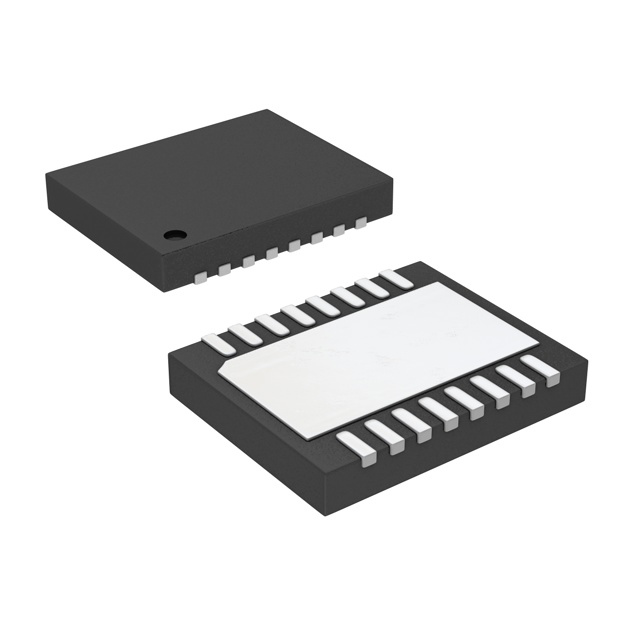
HVSON16 plastic thermal enhanced very thin small outline
SOT1371-1
package; no leads;16 terminals; body 4 6 0.85 mm
4. Limiting values
Table 4.
Limiting values
In accordance with the Absolute Maximum Rating System (IEC 60134).
Symbol
Parameter
Min
Max
Unit
VDS
drain-source voltage
Conditions
-
65
V
VGS
gate-source voltage
0.5
+13
V
Tstg
storage temperature
65
+150
C
Tj
junction temperature
-
225
C
5. Thermal characteristics
Table 5.
Thermal characteristics
Symbol Parameter
Rth(j-c)
BLP8G27-5
Product data sheet
Conditions
thermal resistance from junction to case Tcase = 80 C; PL = 1 W
All information provided in this document is subject to legal disclaimers.
Rev. 2 — 1 October 2015
Typ
Unit
6.4
K/W
© Ampleon Netherlands B.V. 2016. All rights reserved.
2 of 13
�BLP8G27-5
Power LDMOS transistor
6. Characteristics
Table 6.
DC characteristics
Tj = 25 C; unless otherwise specified.
Symbol Parameter
Conditions
V(BR)DSS drain-source breakdown voltage VGS = 0 V; ID = 0.09 mA
Min
Typ
Max
Unit
65
-
-
V
VGS(th)
gate-source threshold voltage
VDS = 10 V; ID = 9 mA
1.5
1.9
2.3
V
IDSS
drain leakage current
VGS = 0 V; VDS = 28 V
1.4
-
+1.4
A
IDSX
drain cut-off current
VGS = VGS(th) + 3.75 V
-
1.6
-
A
IGSS
gate leakage current
VGS = 11 V; VDS = 0 V
-
-
140
nA
gfs
forward transconductance
VDS = 10 V; ID = 9 mA
-
80
-
mS
RDS(on)
drain-source on-state resistance VGS = VGS(th) + 3.75 V;
VDS = 10 V; ID = 315 mA
-
2
-
Table 7.
RF characteristics
A derivative functional RF test is performed in production. The performance as mentioned below is
verified by design and characterization in an NXP class-AB application board.
Test signal: pulsed CW; = 10%; tp = 100 s; VDS = 28 V; IDq = 55 mA; Tcase = 25 C; f = 2140 MHz
Symbol Parameter
BLP8G27-5
Product data sheet
Conditions
Min
Typ
Max
Unit
Gp
power gain
PL(AV) = 0.75 W
17
18
-
dB
D
drain efficiency
PL(AV) = 0.75 W
15
17
-
%
PL(1dB)
output power at 1 dB gain compression
5
-
-
W
All information provided in this document is subject to legal disclaimers.
Rev. 2 — 1 October 2015
© Ampleon Netherlands B.V. 2016. All rights reserved.
3 of 13
�BLP8G27-5
Power LDMOS transistor
7. Application information
7.1 Application circuit
C12
RP1
PC2
PC1
Q1
R1
R8
C14
R2
R4
C13
L1
R3
R5
R6
R7
C8
C9
C15
R11
R9
C10
C11
C1
C3
Q2
C7
R10
C4
C2
C5
C6
Q3
BLP8G27-05
2496-2690 MHz
20R04350B [ V2 ]
aaa-019848
Printed-Circuit Board (PCB): Rogers RO4350B; r = 3.5; thickness = 0.508 mm; thickness copper
plating = 35 m.
See Table 8 for list of components.
Fig 1.
Component layout
Table 8.
List of components
See Figure 1 for component layout.
Component
BLP8G27-5
Product data sheet
Description
Value
Remarks
C1, C2, C3, C4 multilayer ceramic chip capacitor
12 pF
ATC 100A
C5
multilayer ceramic chip capacitor
3 pF
ATC 100A
C6
multilayer ceramic chip capacitor
1.9 pF
ATC 100A
C7, C8, C9,
C10
multilayer ceramic chip capacitor
100 nF, 50 V
Murata:
GRM21BR71H104KA01L
C11, C12, C13
multilayer ceramic chip capacitor
4.7 F, 50 V
Murata:
GRM32ER71H475KA88L
C14, C15
multilayer ceramic chip capacitor
10 F
AVX
RP1
potentiometer
10 turns
R1
chip resistor
75
All information provided in this document is subject to legal disclaimers.
Rev. 2 — 1 October 2015
SMD 0805
© Ampleon Netherlands B.V. 2016. All rights reserved.
4 of 13
�BLP8G27-5
Power LDMOS transistor
Table 8.
List of components …continued
See Figure 1 for component layout.
BLP8G27-5
Product data sheet
Component
Description
Value
Remarks
R2, R3
chip resistor
430
SMD 0805
R4
chip resistor
2 k
SMD 0805
R5
chip resistor
11 k
SMD 0805
R6
chip resistor
1.1 k
SMD 0805
R7
chip resistor
2.0 k
SMD 0805
R8
chip resistor
9.1
SMD 0805
R9
chip resistor
5.1
SMD 0805
R10
chip resistor
910
SMD 0805
R11
chip resistor
500 , 1/4 W
leaded
L1
ferrite bead
1 F, 50 V
Murata:
GRM31MR71H105KA88L
Q1
surface-mounted package
-
SOT89
Q2
transistor
-
PMBT2222A
Q3
transistor
-
BLP8G27-5
PC1
power connector
-
positive supply
PC2
power connector
-
negative supply
All information provided in this document is subject to legal disclaimers.
Rev. 2 — 1 October 2015
© Ampleon Netherlands B.V. 2016. All rights reserved.
5 of 13
�BLP8G27-5
Power LDMOS transistor
7.2 Graphical data
7.2.1 Pulsed CW
aaa-017901
24
70
Gp
Gp
(dB)
60
(1)
(1)
(2)
(2)
(3)
(3)
16
ηD
(%)
Gp
22
50
50
(1)
(1)
(2)
(2)
(3)
(3)
20
12
40
40
18
ηD
8
30
4
20
0
2
4
6
8
PL (W)
30
ηD
16
10
0
20
14
10
10
0
VDS = 28 V; IDq = 55 mA; Tcase = 25 C; = 10 %;
tp = 100 s.
2
4
(1) IDq = 45 mA
(2) f = 2140 MHz
(2) IDq = 55 mA
(3) f = 2170 MHz
(3) IDq = 65 mA
Power gain and drain efficiency as function of
output power; typical values
Fig 3.
aaa-017903
10
70
Gp
ηD
(%)
20
60
(1)
(1)
(2)
(2)
(3)
(3)
16
50
12
40
8
8
PL (W)
Power gain and drain efficiency as function of
output power; typical values
24
Gp
(dB)
6
VDS = 28 V; Tcase = 25 C; f = 2140 MHz; = 10 %;
tp = 100 s.
(1) f = 2110 MHz
Fig 2.
60
Gp
(dB)
ηD
(%)
20
aaa-017902
24
30
ηD
4
20
0
10
0
2
4
6
8
PL (W)
10
VDS = 28 V; IDq = 55 mA; f = 2140 MHz; = 10 %; tp = 100 s.
(1) Tcase = 37 C
(2) Tcase = +25 C
(3) Tcase = +85 C
Fig 4.
Power gain and drain efficiency as function of output power; typical values
BLP8G27-5
Product data sheet
All information provided in this document is subject to legal disclaimers.
Rev. 2 — 1 October 2015
© Ampleon Netherlands B.V. 2016. All rights reserved.
6 of 13
�BLP8G27-5
Power LDMOS transistor
7.2.2 2-Carrier W-CDMA
aaa-017904
24
50
Gp
(dB)
ηD
(%)
(1)
(2)
(3)
22
Gp
20
40
30
(1)
(2)
(3)
ηD
18
20
16
10
14
0
0
1
2
3
4
PL (W)
5
VDS = 28 V; IDq = 55 mA; Tcase = 25 C; carrier spacing = 5 MHz; 46 % clipping; PAR = 8.4 dB at 0.01 % probability on CCDF.
(1) f = 2110 MHz
(2) f = 2140 MHz
(3) f = 2170 MHz
Fig 5.
Power gain and drain efficiency as function of output power; typical values
aaa-017905
0
ACPR5M
(dBc)
-10
aaa-017906
0
ACPR5M
(dBc)
-10
-20
-20
-30
(1)
(2)
(3)
-30
(1)
(2)
(3)
-40
-40
-50
-50
-60
-60
0
0.5
1
1.5
2
2.5
3
3.5
PL(AV) (W)
4
0
VDS = 28 V; IDq = 55 mA; Tcase = 25 C;
carrier spacing = 5 MHz; 46 % clipping; PAR = 8.4 dB at
0.01 % probability on CCDF.
0.5
1
(2) Tcase = +25 C
(3) f = 2170 MHz
(3) Tcase = +85 C
Adjacent channel power ratio (5 MHz) as a
function of average output power; typical
values
Product data sheet
2.5
3
3.5
PL(AV) (W)
4
VDS = 28 V; IDq = 55 mA; f = 2140 MHz;
carrier spacing = 5 MHz; 46 % clipping; PAR = 8.4 dB at
0.01 % probability on CCDF.
(2) f = 2140 MHz
BLP8G27-5
2
(1) Tcase = 37 C
(1) f = 2110 MHz
Fig 6.
1.5
Fig 7.
Adjacent channel power ratio (5 MHz) as a
function of average output power; typical
values
All information provided in this document is subject to legal disclaimers.
Rev. 2 — 1 October 2015
© Ampleon Netherlands B.V. 2016. All rights reserved.
7 of 13
�BLP8G27-5
Power LDMOS transistor
8. Test information
8.1 Ruggedness in class-AB operation
The BLP8G27-5 is capable of withstanding a load mismatch corresponding to
VSWR = 10 : 1 through all phases under the following conditions: VDS = 28 V;
IDq = 55 mA; PL = 1 W; frequency from 700 MHz to 2700 MHz.
BLP8G27-5
Product data sheet
All information provided in this document is subject to legal disclaimers.
Rev. 2 — 1 October 2015
© Ampleon Netherlands B.V. 2016. All rights reserved.
8 of 13
�BLP8G27-5
Power LDMOS transistor
9. Package outline
HVSON16: plastic thermal enhanced very thin small outline package; no leads;
16 terminals; body 4 x 6 x 0.85 mm
SOT1371-1
X
D
B
A
A
E
A1
C
detail X
e3
terminal 1
index area
e2
e1
terminal 1
index area
v
w
b
1/2 e
C A B
C
C
y1 C
e
1
y
8
L
k
Eh
16
9
Dh
0
5 mm
scale
Dimensions (mm are the original dimensions)
Unit
mm
A
A1
b
max 1.00 0.05 0.35
nom 0.85 0.03 0.30
min 0.80 0.00 0.25
C
D(1)
Dh
E(1)
Eh
e
e1
e2
e3
L
k
v
0.2
6.1
6.0
5.9
5.2
5.1
5.0
4.1
4.0
3.9
2.0
1.9
1.8
0.8
0.65
4.0
5.3
0.5
0.4
0.3
0.70
0.65
0.60
0.1
w
y
0.05 0.05
Note
1. Plastic or metal protrusions of 0.075 mm maximum per side are not included.
Outline
version
SOT1371-1
Fig 8.
References
IEC
JEDEC
JEITA
y1
0.1
sot1371-1_po
European
projection
Issue date
14-05-19
14-08-26
MO-229
Package outline SOT1371-1 (HVSON16)
BLP8G27-5
Product data sheet
All information provided in this document is subject to legal disclaimers.
Rev. 2 — 1 October 2015
© Ampleon Netherlands B.V. 2016. All rights reserved.
9 of 13
�BLP8G27-5
Power LDMOS transistor
10. Handling information
CAUTION
This device is sensitive to ElectroStatic Discharge (ESD). Observe precautions for handling
electrostatic sensitive devices.
Such precautions are described in the ANSI/ESD S20.20, IEC/ST 61340-5, JESD625-A or
equivalent standards.
11. Abbreviations
Table 9.
Abbreviations
Acronym
Description
CCDF
Complementary Cumulative Distribution Function
CDMA
Code Division Multiple Access
CW
Continuous Wave
EDGE
Enhanced Data rates for GSM Evolution
ESD
ElectroStatic Discharge
GSM
Global System for Mobile Communication
LDMOS
Laterally Diffused Metal-Oxide Semiconductor
LTE
Long Term Evolution
MC-GSM
Multi Carrier GSM
PAR
Peak-to-Average Ratio
SMD
Surface Mounted Device
VSWR
Voltage Standing-Wave Ratio
W-CDMA
Wideband Code Division Multiple Access
WiMAX
Worldwide Interoperability for Microwave Access
12. Revision history
Table 10.
Revision history
Document ID
Release date
Data sheet status
Change notice
Supersedes
BLP8G27-5 v.2
20151001
Product data sheet
-
BLP8G27-5 v.1
Modifications:
BLP8G27-5 v.1
BLP8G27-5
Product data sheet
•
The format of this document has been redesigned to comply with the new identity guidelines
of Ampleon
•
Legal texts have been adapted to the new company name where appropriate
20150915
Product data sheet
-
All information provided in this document is subject to legal disclaimers.
Rev. 2 — 1 October 2015
-
© Ampleon Netherlands B.V. 2016. All rights reserved.
10 of 13
�BLP8G27-5
Power LDMOS transistor
13. Legal information
13.1 Data sheet status
Document status[1][2]
Product status[3]
Definition
Objective [short] data sheet
Development
This document contains data from the objective specification for product development.
Preliminary [short] data sheet
Qualification
This document contains data from the preliminary specification.
Product [short] data sheet
Production
This document contains the product specification.
[1]
Please consult the most recently issued document before initiating or completing a design.
[2]
The term ‘short data sheet’ is explained in section “Definitions”.
[3]
The product status of device(s) described in this document may have changed since this document was published and may differ in case of multiple devices. The latest product status
information is available on the Internet at URL http://www.ampleon.com.
13.2 Definitions
Draft — The document is a draft version only. The content is still under
internal review and subject to formal approval, which may result in
modifications or additions. Ampleon does not give any representations or
warranties as to the accuracy or completeness of information included herein
and shall have no liability for the consequences of use of such information.
Short data sheet — A short data sheet is an extract from a full data sheet
with the same product type number(s) and title. A short data sheet is intended
for quick reference only and should not be relied upon to contain detailed and
full information. For detailed and full information see the relevant full data
sheet, which is available on request via the local Ampleon sales office. In
case of any inconsistency or conflict with the short data sheet, the full data
sheet shall prevail.
Product specification — The information and data provided in a Product
data sheet shall define the specification of the product as agreed between
Ampleon and its customer, unless Ampleon and customer have explicitly
agreed otherwise in writing. In no event however, shall an agreement be valid
in which the Ampleon product is deemed to offer functions and qualities
beyond those described in the Product data sheet.
13.3 Disclaimers
Limited warranty and liability — Information in this document is believed to
be accurate and reliable. However, Ampleon does not give any
representations or warranties, expressed or implied, as to the accuracy or
completeness of such information and shall have no liability for the
consequences of use of such information. Ampleon takes no responsibility for
the content in this document if provided by an information source outside of
Ampleon.
In no event shall Ampleon be liable for any indirect, incidental, punitive,
special or consequential damages (including - without limitation - lost profits,
lost savings, business interruption, costs related to the removal or
replacement of any products or rework charges) whether or not such
damages are based on tort (including negligence), warranty, breach of
contract or any other legal theory.
Notwithstanding any damages that customer might incur for any reason
whatsoever, Ampleon’s aggregate and cumulative liability towards customer
for the products described herein shall be limited in accordance with the
Terms and conditions of commercial sale of Ampleon.
Right to make changes — Ampleon reserves the right to make changes to
information published in this document, including without limitation
specifications and product descriptions, at any time and without notice. This
document supersedes and replaces all information supplied prior to the
publication hereof.
Suitability for use — Ampleon products are not designed, authorized or
warranted to be suitable for use in life support, life-critical or safety-critical
systems or equipment, nor in applications where failure or malfunction of an
BLP8G27-5
Product data sheet
Ampleon product can reasonably be expected to result in personal injury,
death or severe property or environmental damage. Ampleon and its
suppliers accept no liability for inclusion and/or use of Ampleon products in
such equipment or applications and therefore such inclusion and/or use is at
the customer’s own risk.
Applications — Applications that are described herein for any of these
products are for illustrative purposes only. Ampleon makes no representation
or warranty that such applications will be suitable for the specified use without
further testing or modification.
Customers are responsible for the design and operation of their applications
and products using Ampleon products, and Ampleon accepts no liability for
any assistance with applications or customer product design. It is customer’s
sole responsibility to determine whether the Ampleon product is suitable and
fit for the customer’s applications and products planned, as well as for the
planned application and use of customer’s third party customer(s). Customers
should provide appropriate design and operating safeguards to minimize the
risks associated with their applications and products.
Ampleon does not accept any liability related to any default, damage, costs or
problem which is based on any weakness or default in the customer’s
applications or products, or the application or use by customer’s third party
customer(s). Customer is responsible for doing all necessary testing for the
customer’s applications and products using Ampleon products in order to
avoid a default of the applications and the products or of the application or
use by customer’s third party customer(s). Ampleon does not accept any
liability in this respect.
Limiting values — Stress above one or more limiting values (as defined in
the Absolute Maximum Ratings System of IEC 60134) will cause permanent
damage to the device. Limiting values are stress ratings only and (proper)
operation of the device at these or any other conditions above those given in
the Recommended operating conditions section (if present) or the
Characteristics sections of this document is not warranted. Constant or
repeated exposure to limiting values will permanently and irreversibly affect
the quality and reliability of the device.
Terms and conditions of commercial sale — Ampleon products are sold
subject to the general terms and conditions of commercial sale, as published
at http://www.ampleon.com/terms, unless otherwise agreed in a valid written
individual agreement. In case an individual agreement is concluded only the
terms and conditions of the respective agreement shall apply. Ampleon
hereby expressly objects to applying the customer’s general terms and
conditions with regard to the purchase of Ampleon products by customer.
No offer to sell or license — Nothing in this document may be interpreted or
construed as an offer to sell products that is open for acceptance or the grant,
conveyance or implication of any license under any copyrights, patents or
other industrial or intellectual property rights.
Export control — This document as well as the item(s) described herein
may be subject to export control regulations. Export might require a prior
authorization from competent authorities.
All information provided in this document is subject to legal disclaimers.
Rev. 2 — 1 October 2015
© Ampleon Netherlands B.V. 2016. All rights reserved.
11 of 13
�BLP8G27-5
Power LDMOS transistor
Non-automotive qualified products — Unless this data sheet expressly
states that this specific Ampleon product is automotive qualified, the product
is not suitable for automotive use. It is neither qualified nor tested in
accordance with automotive testing or application requirements. Ampleon
accepts no liability for inclusion and/or use of non-automotive qualified
products in automotive equipment or applications.
In the event that customer uses the product for design-in and use in
automotive applications to automotive specifications and standards, customer
(a) shall use the product without Ampleon’ warranty of the product for such
automotive applications, use and specifications, and (b) whenever customer
uses the product for automotive applications beyond Ampleon’ specifications
such use shall be solely at customer’s own risk, and (c) customer fully
indemnifies Ampleon for any liability, damages or failed product claims
resulting from customer design and use of the product for automotive
applications beyond Ampleon’ standard warranty and Ampleon’ product
specifications.
Translations — A non-English (translated) version of a document is for
reference only. The English version shall prevail in case of any discrepancy
between the translated and English versions.
13.4 Trademarks
Notice: All referenced brands, product names, service names and trademarks
are the property of their respective owners.
Any reference or use of any ‘NXP’ trademark in this document or in or on the
surface of Ampleon products does not result in any claim, liability or
entitlement vis-à-vis the owner of this trademark. Ampleon is no longer part of
the NXP group of companies and any reference to or use of the ‘NXP’
trademarks will be replaced by reference to or use of Ampleon’s own
trademarks.
14. Contact information
For more information, please visit: http://www.ampleon.com
For sales office addresses, please visit: http://www.ampleon.com/sales
BLP8G27-5
Product data sheet
All information provided in this document is subject to legal disclaimers.
Rev. 2 — 1 October 2015
© Ampleon Netherlands B.V. 2016. All rights reserved.
12 of 13
�BLP8G27-5
Power LDMOS transistor
15. Contents
1
1.1
1.2
1.3
2
3
4
5
6
7
7.1
7.2
7.2.1
7.2.2
8
8.1
9
10
11
12
13
13.1
13.2
13.3
13.4
14
15
Product profile . . . . . . . . . . . . . . . . . . . . . . . . . . 1
General description . . . . . . . . . . . . . . . . . . . . . 1
Features and benefits . . . . . . . . . . . . . . . . . . . . 1
Applications . . . . . . . . . . . . . . . . . . . . . . . . . . . 1
Pinning information . . . . . . . . . . . . . . . . . . . . . . 2
Ordering information . . . . . . . . . . . . . . . . . . . . . 2
Limiting values. . . . . . . . . . . . . . . . . . . . . . . . . . 2
Thermal characteristics . . . . . . . . . . . . . . . . . . 2
Characteristics . . . . . . . . . . . . . . . . . . . . . . . . . . 3
Application information. . . . . . . . . . . . . . . . . . . 4
Application circuit . . . . . . . . . . . . . . . . . . . . . . . 4
Graphical data . . . . . . . . . . . . . . . . . . . . . . . . . 6
Pulsed CW . . . . . . . . . . . . . . . . . . . . . . . . . . . . 6
2-Carrier W-CDMA . . . . . . . . . . . . . . . . . . . . . . 7
Test information . . . . . . . . . . . . . . . . . . . . . . . . . 8
Ruggedness in class-AB operation . . . . . . . . . 8
Package outline . . . . . . . . . . . . . . . . . . . . . . . . . 9
Handling information. . . . . . . . . . . . . . . . . . . . 10
Abbreviations . . . . . . . . . . . . . . . . . . . . . . . . . . 10
Revision history . . . . . . . . . . . . . . . . . . . . . . . . 10
Legal information. . . . . . . . . . . . . . . . . . . . . . . 11
Data sheet status . . . . . . . . . . . . . . . . . . . . . . 11
Definitions . . . . . . . . . . . . . . . . . . . . . . . . . . . . 11
Disclaimers . . . . . . . . . . . . . . . . . . . . . . . . . . . 11
Trademarks. . . . . . . . . . . . . . . . . . . . . . . . . . . 12
Contact information. . . . . . . . . . . . . . . . . . . . . 12
Contents . . . . . . . . . . . . . . . . . . . . . . . . . . . . . . 13
Please be aware that important notices concerning this document and the product(s)
described herein, have been included in section ‘Legal information’.
© Ampleon Netherlands B.V. 2016.
All rights reserved.
For more information, please visit: http://www.ampleon.com
For sales office addresses, please visit: http://www.ampleon.com/sales
Date of release: 1 October 2015
Document identifier: BLP8G27-5
�


 工商网监
湘ICP备2023018690号
工商网监
湘ICP备2023018690号
