Environmental Specifications.............................. 2
Equivalent Circuit ............................................... 2
Performance Characteristics............................... 3
I2C & SPI Electrical Parameters .......................... 4
Pressure Output Transfer Function ..................... 4
Temperature Output Transfer Function .............. 4
Device Options ................................................... 5
Operation Overview ........................................ 6-7
Digital Interface Command & Data Formats ... 7-8
I2C Interface.................................................... 8-9
The digital interface eases integration of the sensors into a
wide range of process control and measurement systems,
allowing direct connection to serial communications channels. For battery-powered systems, the sensors can enter very
low-power mode between readings to minimize load on the
power supply.
These calibrated and compensated sensors provide accurate,
stable output over a wide temperature range. This series is
intended for use with non-corrosive, non-ionic working fluids such as air, dry gases and the like. A protective parylene
coating is optionally available for moisture/harsh media
protection.
https://www.allsensors.com/products/dlhr-series
SPI Interface ..................................................9-10
Interface Timing Diagrams ............................... 11
How to Order Guide ........................................ 12
Dimensional Package Drawings
SIP ...............................................................13-14
DIP ..............................................................15-16
SMT .................................................................. 17
Suggested Pad Layout ....................................... 18
Product Labeling ............................................... 18
Soldering Recommendations ............................ 18
All Sensors
f 408 225 2079
Pressure Sensor Maximum Ratings ..................... 2
The DLHR Series Mini Digital Output Sensor is based on
All Sensors’ CoBeam2 TM Technology. This reduces package
stress susceptibility, resulting in improved overall long term
stability and vastly improves the position sensitivity.
p 408 225 4314
Features & Applications ...................................... 2
Standard Pressure Ranges ................................... 2
Introduction
a 16035 Vineyard Blvd. Morgan Hill, CA 95037
Table of Contents
e www.allsensors.com
all sensors
DLHR - Low Voltage Digital Pressure Sensors Series
DS-0350 Rev C
Page 1 of 18
�Applications
• 0.5 to 60 inH2O Pressure Ranges
• 1.68V to 3.6V Supply Voltage Range
• I2C or SPI Interface (Automatically Selected)
• Better than 0.25% Accuracy
• High Resolution 16/17/18 bit Output
• Medical Breathing
• Environmental Controls
• HVAC
• Industrial Controls
• Portable/Hand-Held Equipment
Standard Pressure Ranges
inH2O
Burst Pressure
kPa
inH2O
Nominal Span
kPa
Counts
DLHR-F50D
± 0.5
125
100
25
300
75
±0.4 * 224
DLHR-L01D
±1
250
100
25
300
75
±0.4 * 224
DLHR-L02D
±2
500
100
25
300
75
±0.4 * 224
DLHR-L05D
±5
1,250
200
50
300
75
±0.4 * 224
DLHR-L10D
± 10
2,500
200
50
300
75
±0.4 * 2
DLHR-L20D
± 20
5,000
200
50
500
125
±0.4 * 2
DLHR-L30D
± 30
7,500
200
50
500
125
±0.4 * 2
DLHR-L60D
± 60
15,000
200
50
800
200
±0.4 * 2
24
24
24
24
24
DLHR-L01G
0 to 1
250
100
25
300
75
0.8 * 2
DLHR-L02G
0 to 2
500
100
25
300
75
0.8 * 2
DLHR-L05G
0 to 5
1,250
200
50
300
75
0.8 * 2
DLHR-L10G
0 to 10
2,500
200
50
300
75
0.8 * 2
DLHR-L20G
0 to 20
5,000
200
50
500
125
0.8 * 2
DLHR-L30G
0 to 30
7,500
200
50
500
125
0.8 * 2
DLHR-L60G
0 to 60
15,000
200
50
800
200
0.8 * 2
24
24
24
24
24
24
Note A: Operating range in Pa is expressed as an approximate value.
Pressure Sensor Maximum Ratings
Supply Voltage (Vs)
Absolute Maximum
Recommended
3.63 Vdc
1.75 to 3.60 Vdc
Common Mode Pressure
10 psig
Lead Temperature (soldering 2-4 sec.)
270 °C
Environmental Specifications
Temperature Ranges
Compensated:
Commercial
Industrial
0°C to 70°C
-20°C to 85°C
-25°C to 85 °C
-40°C to 125 °C
Humidity Limits (non condensing)
0 to 95% RH
Operating
Storage
Equivalent Circuit
Vs
SCL
I2C
SDA
- OR -
EOC
Table of Contents
Vs
SCLK
MISO
MOSI
/SS
EOC
Gnd
Gnd
All Sensors
SPI
f 408 225 2079
Pa
DS-0350 Rev C
Page 2 of 18
p 408 225 4314
Proof Pressure
inH2O
a 16035 Vineyard Blvd. Morgan Hill, CA 95037
Operating Range A
Device
e www.allsensors.com
Features
all sensors
DLHR Series Low Voltage Digital Pressure Sensors
�Performance Characteristics for DLHR Series - Commercial and Industrial Temperature Range
All parameters are measured at 3.3V ±5% excitation and 25C unless otherwise specified (Note 9). Pressure measurements are with positive
pressure applied to PORT B.
Parameter
Output Span (FSS)
LxxD, FxxD
LxxG
Offset Output @ Zero Diff. Pressure (Osdig)
LxxD, FxxD
LxxG
Total Error Band
F50D
L01x
L02x
L05x
L10x, L20x, L30x, L60x
Span Temperature Shift
F50x, L01x, L02x
L05x, L10x, L20x, L30x, L60x
Offset Temperature Shift
F50x, L01x, L02x
L05x, L10x, L20x, L30x, L60x
Offset Warm-up Shift
F50x, L01x, L02x
L05x, L10x, L20x, L30x, L60x
Offset Position Sensitivity (±1g)
F50x, L01x, L02x
L05x, L10x, L20x, L30x, L60x
Offset Long Term Drift (One Year)
F50x, L01x, L02x
L05x, L10x, L20x, L30x, L60x
Linearity, Hysteresis Error
FxxD, LxxD
LxxG
Pressure Digital Resolution - No Missing Codes
16-bit Option
17-bit Option
18-bit Option
Temperature Output
Resolution
Overall Accuracy
Supply Current Requirement
During Active State (ICCActive)
During Idle State (ICCIdle)
Power On Delay
Data Update Time (tDU)
Min
Typ
Max
Units
Notes
-
±0.4 * 224
0.8 * 224
-
Dec Counts
Dec Counts
1
1
-
0.5 * 224
0.1 * 224
-
Dec Counts
Dec Counts
-
-
±0.35
±0.25
±0.25
±0.20
±0.15
±1.50
±1.00
±0.75
±0.75
±0.75
%FSS
%FSS
%FSS
%FSS
%FSS
2
2
2
2
2
-
±0.5
±0.2
-
%FSS
%FSS
3
3
-
±0.5
±0.2
-
%FSS
%FSS
3
3
-
±0.25
±0.15
-
%FSS
%FSS
4
4
-
±0.10
±0.05
-
%FSS
%FSS
-
-
±0.25
±0.15
-
%FSS
%FSS
-
-
±0.25
±0.10
-
%FSS
%FSS
6
6
15.7
16.7
17.7
-
-
bit
bit
bit
-
-
16
2
-
bit
°C
-
-
2
100
-
2.6
250
2.5
mA
nA
ms
5, 7, 8
5, 7, 8
5
ms
5, 7
(see table below)
DLHR Series Low Voltage Digital Pressure Sensors
Table of Contents
Page 3 of 18
�Symbol
Min
Typ
Max
Units
Notes
Input High Level
-
80
-
100
% of Vs
5
Input Low Level
-
0
-
20
% of Vs
5
Output Low Level
-
-
-
10
% of Vs
5
I2C Pull-Up Resistor
-
1,000
-
-
Ω
5
I2C Load Capacitance on SDA, @ 400 kHz
I2C Input Capacitance (each pin)
CSDA
-
-
200
pF
5
CI2C_IN
-
-
10
pF
5
-
-
41
-
decimal
-
I2C Address
Pressure Output Transfer Function
Is the sensor 24‐bit digital output.
�����
Is the specified digital offset
For Gage Operating Range sensors:
For Differential Operating Range sensors:
�������� ��
The sensor Full Scale Span in inches H2O
For Gage Operating Range sensors: Full Scale Pressure
For Differential Operating Range sensors: 2 x Full Scale Pressure.
e www.allsensors.com
�������
������� � �����
� � �������� ��
2��
0.1 * 224
0.5 * 224
f 408 225 2079
Where:
������������� �� � ��2� � �
Temperature Output Transfer Function
������� ∗ 125
� � ��
2��
p 408 225 4314
����������� ��� � �
Where:
�������
The sensor 24‐bit digital temperature output.
(Note that only the upper 16 bits are significant)
Specification Notes
note
1: THE SPAN IS THE ALGEBRAIC DIFFERENCE BETWEEN FULL SCALE DECIMAL COUNTS AND THE OFFSET DECIMAL COUNTS. THE FULL SCALE PRESSURE IS THE
note
2: TOTAL ERROR BAND CONSISTS OF OFFSET AND SPAN TEMPERATURE AND CALIBRATION ERRORS, LINEARITY AND PRESSURE HYSTERESIS ERRORS, OFFSET
note
3: SHIFT IS RELATIVE TO 25C.
note
4: SHIFT IS WITHIN THE FIRST HOUR OF EXCITATION APPLIED TO THE DEVICE.
note
5: PARAMETER IS CHARACTERIZED AND NOT 100% TESTED.
note
6: MEASURED AT ONE-HALF FULL SCALE RATED PRESSURE USING BEST STRAIGHT LINE CURVE FIT.
note
7: DATA UPDATE TIME IS EXCLUSIVE OF COMMUNICATIONS, FROM COMMAND RECEIVED TO END OF BUSY STATUS. THIS CAN BE OBSERVED AS EOC PIN
note
8: AVERAGE CURRENT CAN BE ESTIMATED AS : ICCIdle + (tDU / Reading Interval) * ICCActive). REFER TO FIGURE 2 FOR ACTIVE AND IDLE CONDITIONS OF THE
note
9: THE SENSOR IS CALIBRATED WITH A 3.3V SUPPLY HOWEVER, AN INTERNAL REGULATOR ALLOWS A SUPPLY VOLTAGE OF 1.68V TO 3.6V TO BE USED
MAXIMUM POSITIVE CALIBRATED PRESSURE.
WARM-UP SHIFT, OFFSET POSITION SENSITIVITY AND LONG TERM OFFSET DRIFT ERRORS.
LOW- STATE DURATION.
SENSOR (THE ACTIVE STATE IS WHILE EOC PIN IS LOW).
WITHOUT AFFECTING THE OVERALL SPECIFICATIONS. THIS ALLOWS DIRECT OPERATION FROM A BATTERY SUPPLY.
All Sensors
Table of Contents
DS-0350 Rev C
Page 4 of 18
a 16035 Vineyard Blvd. Morgan Hill, CA 95037
Parameter
all sensors
I2C / SPI Electrical Parameters for DLHR Series
�Device Options
Output Resolution
Calibrated output resolution can be ordered to be 16, 17, or 18 bits.
Higher resolution results in slower update times; see the Data Update Time in the Performance Characteristics table.
Coating
Parylene Coating: Parylene coating provides a moisture barrier and protection form some harsh media. Consult factory
for applicability of Parylene for the target application and sensor type. This option is not available for pressure ranges
below 10 inH2O.
DLHR Series Low Voltage Digital Pressure Sensors
Table of Contents
Page 5 of 18
�Operation Overview
The DLHR is a digital sensor with a signal path that includes a sensing element, a variable- bit analog to digital
converter, a DSP and an IO block that supports either an I2C or SPI interface (see Figure 1 below). The sensor also
includes an internal temperature reference and associated control logic to support the configured operating mode.
Since there is a single ADC, there is also a multiplexer at the front end of the ADC that selects the signal source for the
ADC.
After completion of the measurement, the result may then be read using the Data Read command. The ADC and DSP
remain in Idle state, and the I/O block returns the 7 bytes of status and measurement data. See Figure 2, following. At
any time, the host may request current device status with the Status Read command. (See Table 1 for a summary of all
commands.)
For optimum sensor performance, All Sensors recommends that Measurement commands be issued at a fixed interval
by the host system. Irregular request intervals may increase overall noise on the output.
Furthermore, if reading intervals are much slower than the Device Update Time, using the Averaging commands is
suggested to reduce offset shift. This shift is constant with respect to time interval, and may be removed by the application. For longer fixed reading intervals, this shift may be removed by the factory on special request.
I/O Interface Configuration: The sensor automatically selects SPI or I2C serial interface, based on the following protocol: If the /SS input is set low by the host (as occurs during a SPI command transaction), the I/O interface will remain
configured for SPI communications until power is removed. Otherwise, once a valid device address and command
have been received over the I2C interface, the I/O interface will remain configured for I2C until power is removed.
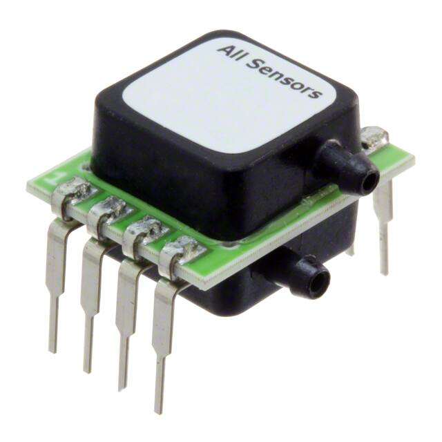
NOTE: The four-pin (SIP) packages only support the I2C interface.
All Sensors
Table of Contents
DS-0350 Rev C
Page 6 of 18
f 408 225 2079
Sensor Commands: Five Measurement commands are supported, returning values of either a single pressure / temperature reading or an average of 2, 4, 8, or 16 readings. Each of these commands wakes the sensor from Idle state into
Active state, and starts a measurement cycle. For the Start-Average commands, this cycle is repeated the appropriate
numper of times, while the Start-Single command performs a single iteration. When the DSP has completed calculations and the new values have been made available to the I/O block, the sensor returns to Idle state. The sensor
remains in this low-power state until another Measurement command is received.
p 408 225 4314
The DSP receives the converted pressure and temperature information and applies a multi-order transfer function to
compensate the pressure output. This transfer function includes compensation for span, offset, temperature effects on
span, temperature effects on offset and second order temperature effects on both span and offset. There is also linearity
compensation for gage devices and front to back linearity compensation for differential devices.
a 16035 Vineyard Blvd. Morgan Hill, CA 95037
The ADC performs conversions on the raw sensor signal (P), the temperature reference (T) and a zero reference (Z)
during the ADC measurement cycle.
e www.allsensors.com
all sensors
Figure 1 - DLHR Essential Model
�Operation Overview cont’d
Figure 2 - DLHR Communication Model
Start-Single Command
Command
Start-Single
Internal State
Idle
Interal Operation
Idle
Data Read
Active
Start-Single
Active
Idle
ADC (Temp, Zero, Pressure)
Idle
DSP
ADC (Temp, Zero, Pressure)
Idle
Idle
DSP
New Data Available
EOC
Start-Average2 / 4 / 8 / 16 Commands (Auto Averaging)
Command
Data Read
Start-Average2/4/8/16
Internal State
Idle
Interal Operation
Idle
Active
ADC (Temp, Zero, Pressure)1
ADC (Temp, Zero, Pressure)n
DSP
Start-Average2/4/8/16
Idle
Active
Idle
ADC (T, Z, P)…
New Data Available
EOC
Digital Interface Command Formats
When requesting the start of a measurement, the command length for I2C is 1 byte, for SPI it is 3 bytes.
When requesting sensor status over I2C, the host simply performs a 1-byte read transfer.
When requesting sensor status over SPI, the host must send the Status Read command byte while reading 1 byte.
When reading sensor data over I2C, the host simply performs a 7-byte read transfer.
When reading sensor data over SPI, the host must send the 7-byte Data Read command while reading the data.
SENDING UNDOCUMENTED COMMANDS TO SENSOR WILL CORRUPT CALIBRATION AND IS NOT COVERED
BY WARRANTY.
See Table 1 below for Measurement Commands, Sensor Data read and Sensor Status read details.
Table 1 - DLHR Sensor Command Set
Measurement Commands
Description
SPI ( 3 bytes )
I2C ( 1 byte)
Start-Single
0xAA
0x00
0x00
0xAA
Start-Average2
0xAC
0x00
0x00
0xAC
Start-Average4
0xAD
0x00
0x00
0xAD
Start-Average8
0xAE
0x00
0x00
0xAE
Start-Average16
0xAF
0x00
0x00
0xAF
Read Sensor Data
I2C Read of 7 bytes from device
Read of 7 bytes from device
SPI Host must send [0xF0], then 6 bytes of [0x00] on MOSI
Sensor Returns 7 bytes on MISO
Read Sensor Status
Read
of
1
byte
from device.
I2C
Read of 1 byte from device
SPI Host must send [0xF0] on MOSI
Sensor Returns 1 byte on MISO
DLHR Series Low Voltage Digital Pressure Sensors
Table of Contents
Page 7 of 18
�Digital Interface Data Format
For either type of digital interface, the format of data returned from the sensor is the same. The first byte consists of
the Status Byte followed by a 24-bit unsigned pressure value and a 24-bit unsigned temperature value. Unused bits
beyond the calibrated bit width are undefined, and may have any value. See the Pressure Output Transfer Function
and Temperature Output Transfer Function definitions on page 3 for converting to pressure and temperature.
Refer to Table 2 for the overall data format of the sensor. Table 3 shows the Status Byte definition.
Note that a completed reading without error will return status 0x40.
P[7:0]
Pressure
Byte 0
T[23:16]
Temperature
Byte 3
T[15:8]
Temperature
Byte 1
T[7:0]
Temperature
Byte 0
Table 3- Status Byte Definition
Description
[Always = 0]
Power : [1 = Power On]
Busy: [ 1 = Processing Command, 0 = Ready]
Mode: [00 = Normal Operation ]
Memory Error [ 1 = EEPROM Checksum Fail]
Sensor Configuration [ always = 0]
ALU Error [1 = Error]
e www.allsensors.com
Bit
Bit 7 [MSB]
6
5
4:3
2
1
Bit 0 [LSB]
I2C Interface
I2C Command Sequence
The part enters Idle state after power-up, and waits for a command from the bus master. Any of the five Measurement
commands may be sent, as shown in Table 1. Following receipt of one of these command bytes, the EOC pin is set
to Low level, and the sensor Busy bit is set in the Status Byte. After completion of measurement and calculation in the
Active state, compensated data is written to the output registers, the EOC pin is set high, and the processing core goes
back to Idle state. The host processor can then perform the Data Read operation, which for I2C is simply a 7-byte
Device Read.
If the EOC pin is not monitored, the host can poll the Status Byte by repeating the Status Read command, which for
I2C is a one-byte Device Read. When the Busy bit in the Status byte is zero, this indicate that valid data is ready, and
a full Data Read of all 7 bytes may be performed.
DO NOT SEND COMMANDS TO SENSOR OTHER THAN THOSE DEFINED IN TABLE 1.
I2C Bus Communications Overview
The I2C interface uses a set of signal sequences for communication. The following is a description of the supported
sequences and their associated mnemonics. Refer to Figure 3 for the associated usage of the following signal sequences.
Bus not Busy (I): During idle periods both data line (SDA) and clock line (SCL) remain HIGH.
START condition (ST): A HIGH to LOW transition of SDA line while the clock (SCL) is HIGH is interpreted as
START condition. START conditions are always set by the master. Each initial request for a pressure value has to
begin with a START condition.
START condition (ST): A HIGH to LOW transition of SDA line while the clock (SCL) is HIGH is interpreted as
START condition. START conditions are always set by the master. Each initial request for a pressure value has to
begin with a START condition.
Slave address (An): The I²C-bus requires a unique address for each device. The DLH sensor has a preconfigured
slave address (see specification table on Page 3). After setting a START condition the master sends the address byte
containing the 7 bit sensor address followed by a data direction bit (R/W). A “0” indicates a transmission from master
to slave (WRITE), a “1” indicates a device-to master request (READ).
All Sensors
Table of Contents
DS-0350 Rev C
Page 8 of 18
f 408 225 2079
P[15:8]
Pressure
Byte 1
p 408 225 4314
P[23:16]
Pressure
Byte 3
a 16035 Vineyard Blvd. Morgan Hill, CA 95037
S[7:0]
Status
Byte
all sensors
Table 2 - Output Data Format
�I2C Interface (Cont’d)
Acknowledge (A or N): Data is transferred in units of 8 bits (1 byte) at a time, MSB first. Each data-receiving
device, whether master or slave, is required to pull the data line LOW to acknowledge receipt of the data. The
Master must generate an extra clock pulse for this purpose. If the receiver does not pull the data line down, a
NACK condition exists, and the slave transmitter becomes inactive. The master determines whether to send
the last command again or to set the STOP condition, ending the transfer.
DATA valid (Dn): State of data line represents valid data when, after a START condition, data line is stable for
duration of HIGH period of clock signal. Data on line must be changed during LOW period of clock signal.
There is one clock pulse per data bit.
STOP condition (P): LOW to HIGH transition of the SDA line while clock (SCL) is HIGH indicates a STOP condition.
STOP conditions are always generated by the master.
Figure 3 - I2C Communication Diagram
1. Measurement Commands: Start-Single ( to start reading of single sample):
Start-Single
C7…C0: 0xAA
Start-Average2
C7…C0: 0xAC
Start-Average4
C7…C0: 0xAD
Start-Average8
C7…C0: 0xAE
Start-Average16
C7…C0: 0xAF
Set by bus master:
Set by sensor:
I
ST A6 A5 A4 A3 A2 A1 A0 W
I
ST A6 A5 A4 A3 A2 A1 A0 R
I
ST A6 A5 A4 A3 A2 A1 A0 R
A
C7 …
C0
N
SP
I
SP
I
2. Status Read:
Set by bus master:
Set by sensor:
A S7 … S0
N
3. Data Read:
Set by bus master:
Set by sensor:
Bus states:
Idle:
Start:
Stop:
Ack:
Nack:
“Read” bit (1):
“Write” bit (0):
I
ST
SP
A
N
R
W
Sensor Address:
A6 … A0
A S7 … S0
A
A
P23 … P16
A
P15 … P8
A
P7 … P0
A
T23 … T16
A
T15 … T8
N SP
I
T7 … T0
Data bits:
Status:
Pressure data:
Temperature data:
S7 … S0
P23 … P0
T23 … T0
Command Bits:
C7 … C0
SPI Interface
SPI Command Sequence
As with the I2C interface configuration, the part enters Idle state after power-up, and waits for a command from the
SPI master. To start a measurement cycle, one of the 3- byte Measurement Commands (see Table 1) must be issued
by the master.
The data returned by the sensor during this command request consists of the Status Byte followed by two undefined
data bytes.
On successful decode of the command, the EOC pin is set Low as the core goes into Active state for measurement
and calculation. When complete, updated sensor data is written to the output registers, and the core goes back to the
Idle state. The EOC pin is set to a High level at this point, and the Busy status bit is set to 0. At any point during the
Active or Idle periods, the SPI master can request the Status Byte by sending a Status Read command (a single byte
with value 0xF0).
As with the I2C configuration, a Busy bit of value 0 in the Status Byte or a high level on the EOC pin indicates that a
valid data set may be read from the sensor. The Data Read command must be sent from the SPI master (The first byte
of value 0xF0 followed by 6 bytes of 0x00).
NOTE: Sending commands that are not defined in Table 1 will corrupt sensor operation.
DLHR Series Low Voltage Digital Pressure Sensors
Table of Contents
Page 9 of 18
�SPI Interface (Cont’d)
SPI Bus Communications Overview
The sequence of bits and bus signals are shown in the following illustration (Figure 4). Refer to Figure 5 in the Interface Timing Diagram section for detailed timing data.
Figure 4 - SPI Communications Diagram
SCLK
all sensors
Measurement Command
--First Command Byte (0xAA / 0xAC / 0xAD / 0xAE / 0xAF)
MOSI XXXX
C23
C22
C21
MISO HI-Z
S7
S6
S5
Lower Command Bytes (0x00 0x00)
C20
C19
C18
C17
C16
C 15
S4
S3
S2
S1
S0
XX
-----
S7 … S0 (Status)
C1
C0
XXXX
XX
XX
HI-Z
(Undefined Data)
SS
e www.allsensors.com
---
Read Status Command
SCLK
Command (0xF0)
MOSI Don't Care
1
1
1
MISO
S7
S6
S5
Hi-Z
1
0
0
0
0
S4
S3
S2
S1
S0
Don't care
Hi-Z
f 408 225 2079
S7 … S0 (Status)
SS
Data Read Command
---
---
p 408 225 4314
SCLK
Don't Care
1
1
1
1
0
0
0
0
MISO
Hi-Z
S7
S6
S5
S4
S3
S2
S1
S0
S7 … S0 (Status)
SS
All Sensors
Table of Contents
0
0
P23 P22
---
0
0
---
P1
P0
0
0
T23 T22
---
0
0
Don't Care
---
T1
T0
Hi-Z
P23…P0 (Pressure)
T23…T0 (Temperature)
---
---
a 16035 Vineyard Blvd. Morgan Hill, CA 95037
Command (0xF0 then 6 bytes of 0x00)
MOSI
DS-0350 Rev C
Page 10 of 18
�Interface Timing Diagrams
Figure 5 - SPI Timing Diagram
tSSCLK
tLOW
tCLKD
tHIGH
SCLK
MISO
MOSI
(HI•Z)
(HI•Z)
don't care
(don't
care)
tSSSO
tDSU
tDH
SS
tSSZ
tCLKSS
PARAMETER
SCLK frequency (1)
SS low to first clock edge
SS low to serial out
Clock to data out
SCLK low width
SCLK high width
Data setup to clock
Data hold after clock
Last clock to rising SS
SS high to output hi-Z
Bus idle time
(1) Maximum by design, tested to 1.0 MHz.
SYMBOL
fSCLK
tSSCLK
tSSSO
tCLKD
tLOW
tHIGH
tDSU
tDH
tCLKSS
tSSZ
tIDLE
MIN
0.05
120
-8
100
100
50
50
0
-250
TYP
-
tIDLE
MAX
5
20
32
20
-
UNITS
MHz
ns
ns
ns
ns
ns
ns
ns
ns
ns
ns
Figure 6 - I2C Timing Diagram
tH STA
tHIGH
tLOW
SCL
SDA
tSUS TA
PARAMETER
SCL frequency
SCL low width
SCL high width
Start condition setup
Start condition hold
Data setup to clock
Data hold to clock
Stop condition setup
Bus idle time
tSUDAT
SYMBOL
fSCL
tLOW
tHIGH
tSUSTA
tHSTA
tSUDAT
tHDAT
tSUSTP
tIDLE
tH DAT
MIN
100
1.3
0.6
0.6
0.6
0.1
0
0.6
2.0
tSUS TP
TYP
-
tIDLE
MAX
400
-
UNITS
KHz
us
us
us
us
us
us
us
us
DLHR Series Low Voltage Digital Pressure Sensors
Table of Contents
Page 11 of 18
�How to Order
Refer to Table 4 for configuring a standard base part number which includes the pressure range, package and temperature range. Table 5 shows the available configuring options. The option identifier is required to complete the
device part number. Refer to Table 6 for the available device packages.
Example P/N with options: DLHR-L02D-E1NS-C-NAV6
Table 4 - How to configure a base part number
Example DLHR - L02D
-
ID
1
2
E
ID
N
B
1
PACKAGE
Lid Style
Description
Non-Barbed
Barbed
ID
S
D
J
N
TEMPERATURE RANGE
Lead Type
Description
SIP (see note 10)
DIP
J-Lead SMT (see note 11)
S
ID
C
I
-
Description
Commercial
Industrial
C
Example
COATING
ID Description
N No Coating
P Parylene Coating (see note 11)
N
ID
A
2
3
4
5
6
7
INTERFACE
Description
Auto I2C, address 0x29/SPI
Auto I2C, address 0x28/SPI
Auto I2C, address 0x38/SPI
Auto I2C, address 0x48/SPI
Auto I2C, address 0x58/SPI
Auto I2C, address 0x68/SPI
Auto I2C, address 0x78/SPI
A
SUPPLY VOLTAGE
ID Description
V 1.68V to 3.6V
V
ID
6
7
8
RESOLUTION
Description
16 Bit
17 bit
18 bit
f 408 225 2079
ORDERING INFORMATION
Table 5 - How to configure an option identifier
6
Table 6 - Available E-Series Package Configurations
Port
Orientation
Non‐Barbed Lid
Lead Style
(1)
SIP
DIP
J Lead SMT
Dual Port
Same Side
Barbed Lid
Lead Style
Low Profile DIP
SIP
(1)
DIP
N/A
E1NS
E1ND
E1NJ
Dual Port
Opposite Side
E1BS
E2ND
E2NJ
E2BS
Specification Notes (Cont.)
note
10: SPI INTERFACE IS ONLY AVAILABLE IN 8-LEAD DIP PACKAGES.
Single Port
N/A
N/A
N/A
N/A
N/A
Note(Gage)
11: PARYLENE COATING NOT OFFERED IN J-LEAD SMT CONFIGURATION.
J Lead SMT
Low Profile DIP
N/A
N/A
N/A
N/A
N/A
N/A
E1BD
N/A
E2NS
E2BD
N/A
(1) SPI is not available in SIP packages
(1) SPI is not available in SIP packages
All Sensors
Table of Contents
all sensors
Description
±0.5 inH2O
±1 inH2O
±2 inH2O
±5 inH2O
±10 inH2O
±20 inH2O
±30 inH2O
±60 inH2O
0 to 1 inH2O
0 to 2 inH2O
0 to 5 inH2O
0 to 10 inH2O
0 to 20 inH2O
0 to 30 inH2O
0 to 60 inH2O
Port Orientation
Description
Dual Port Same Side
Dual Port Opposite Side
e www.allsensors.com
ID
F50D
L01D
L02D
L05D
L10D
L20D
L30D
L60D
L01G
L02G
L05G
L10G
L20G
L30G
L60G
ORDERING INFORMATION
ID
DLHR
Base
ID
E
DS-0350 Rev C
Page 12 of 18
p 408 225 4314
PRESSURE RANGE
a 16035 Vineyard Blvd. Morgan Hill, CA 95037
SERIES
�Package Drawings
E1NS Package
Pinout
1) Gnd
2) Vs
3) SDA
4) SCL
7.17
0.282
12.70
0.500
4.88
0.192
0.64
0.025
10.79
0.425
2.10
0.082
2.04
0.080
10.79
0.425
Port A
2.73
0.107
[9.65]
0.380 (nom)
6.45
0.254
9.80
0.386
15.75
0.620
Port B
0.25
0.010
0.51
0.020
2.54
0.100
Pin 1 2 3 4
NOTES
1)Dimensions are in inches [mm]
2)For suggested pad layout, see drawing: PAD-01
E1BS Package
Pinout
1) Gnd
2) Vs
3) SDA
4) SCL
1.68
0.066
10.80
0.425
Port B
0.25
0.010
Port A
2.73
0.107
[9.65]
0.380 (nom)
6.45
0.254
9.80
0.386
1.14
0.045
10.80
0.425
15.75
0.620
0.64
0.025
2.11
0.083
12.70
0.500
4.88
0.192
0.51
0.020
2.24
0.088
9.15
0.360
2.54
0.100
Pin 1 2 3 4
NOTES
1)Dimensions are in inches [mm]
2)For suggested pad layout, see drawing: PAD-01
DLHR Series Low Voltage Digital Pressure Sensors
Table of Contents
Page 13 of 18
�Package Drawings (Cont’d)
E2NS Package
Pinout
12.70
0.500
2.10
0.082
2.04
0.080
e www.allsensors.com
0.25
0.010
2.54
0.100
0.51
0.020
Pin 1 2 3 4
NOTES
1)Dimensions are in inches [mm]
2)For suggested pad layout, see drawing: PAD-01
E2BS Package
Pinout
1) Gnd
2) Vs
3) SDA
4) SCL
2.12
0.084
1.68
0.066
10.80
0.425
Port B
2.73
0.107
15.75
0.620
[9.65]
0.380 (nom)
9.80
0.386
1.14
0.045
10.80
0.425
Port A
0.25
0.010
2.11
0.083
12.70
0.500
2.24
0.088
9.15
0.360
0.64
0.025
0.51
0.020
2.54
0.100
Pin 1 2 3 4
NOTES
1)Dimensions are in inches [mm]
2)For suggested pad layout, see drawing: PAD-01
All Sensors
Table of Contents
DS-0350 Rev C
Page 14 of 18
f 408 225 2079
10.79
0.425
2.73
0.107
[9.65]
0.380 (nom)
9.80
0.386
15.75
0.620
Port B
p 408 225 4314
10.79
0.425
Port A
a 16035 Vineyard Blvd. Morgan Hill, CA 95037
7.17
0.282
0.64
0.025
2.12
0.084
all sensors
1) Gnd
2) Vs
3) SDA
4) SCL
�Package Drawings (Cont’d)
E1ND Package
Pinout
0.46
0.018
1) Gnd
2) Vs
3) SDA/MOSI
4) SCL/SCLK
5) EOC
6) MISO
7) Not Connected
8) /SS
5.72
0.225
Pin 8 7 6 5
7.17
0.282
0.64
0.025
12.70
0.500
4.88
0.192
10.79
0.425
2.10
0.082
NOTES
1) Dimensions are in inches [mm]
2) For suggested pad layout, see drawing: PAD-03
2.04
0.080
10.79
0.425
15.75
0.620
6.45
0.254
Port A
2.73
0.107
0.25
0.010
1.48
0.058
9.80
0.386
16
0.630
Port B
2.54
0.100
8.89
0.350
(min)
Pin 1 2 3 4
E1BD Package
Pinout
0.46
0.018
1) Gnd
2) Vs
3) SDA/MOSI
4) SCL/SCLK
5) EOC
6) MISO
7) Not Connected
8) /SS
5.72
0.225
Pin 8 7 6 5
9.15
0.360
0.64
0.025
12.70
0.500
4.88
0.192
2.11
0.083
1.14
0.045
10.80
0.425
NOTES
1) Dimensions are in inches [mm]
2) For suggested pad layout, see drawing: PAD-03
8.89
0.350
(min)
2.24
0.088
1.68
0.066
10.80
0.425
15.75
0.620
16
0.630
6.45
0.254
Port A
2.73
0.107
0.25
0.010
1.48
0.058
9.80
0.386
Port B
2.54
0.100
Pin 1 2 3 4
DLHR Series Low Voltage Digital Pressure Sensors
Table of Contents
Page 15 of 18
�Package Drawings (Cont’d)
E2ND Package
0.46
0.018
1) Gnd
2) Vs
3) SDA/MOSI
4) SCL/SCLK
5) EOC
6) MISO
7) Not Connected
8) /SS
5.72
0.225
7.17
0.282
Pin 8 7 6 5
0.64
0.025
12.70
0.500
2.12
0.084
10.79
0.425
Port A
2.10
0.082
all sensors
Pinout
E2BD Package
Pinout
0.46
0.018
1) Gnd
2) Vs
3) SDA/MOSI
4) SCL/SCLK
5) EOC
6) MISO
7) Not Connected
8) /SS
5.72
0.225
Pin 8 7 6 5
9.15
0.360
12.70
0.500
0.64
0.025
NOTES
1) Dimensions are in inches [mm]
2) For suggested pad layout, see drawing: PAD-03
All Sensors
Table of Contents
1.68
0.066
10.80
0.425
15.75
0.620
Port B
2.73
0.107
0.25
0.010
1.48
0.058
9.80
0.386
16
0.630
Port A
8.89
0.350
(min)
1.14
0.045
10.80
0.425
2.24
0.088
2.12
0.084
2.11
0.083
2.54
0.100
Pin 1 2 3 4
DS-0350 Rev C
Page 16 of 18
e www.allsensors.com
Pin 1 2 3 4
f 408 225 2079
NOTES
1) Dimensions are in inches [mm]
2) For suggested pad layout, see drawing: PAD-03
p 408 225 4314
2.54
0.100
a 16035 Vineyard Blvd. Morgan Hill, CA 95037
2.04
0.080
10.79
0.425
2.73
0.107
8.89
0.350
(min)
1.48
0.058
15.75
0.620
0.25
0.010
9.80
0.386
16
0.630
Port B
�Package Drawings (Cont’d)
E1NJ Package
Pinout
1) Gnd
2) Vs
3) SDA/MOSI
4) SCL/SCLK
5) EOC
6) MISO
7) Not Connected
8) /SS
Pin 8 7 6 5
7.17
0.282
0.64
0.025
12.70
0.500
4.88
0.192
2.10
0.082
10.79
0.425
15.75
0.620
2.04
0.080
Port A
2.73
0.107
DETAIL A
SCALE 4 : 1
6.45
0.254
9.80
0.386
1.51
0.059
3.94
0.155
0.81
R0.032
10.79
0.425
Port B
0.25
0.010
A
1.27
0.050
2.54
0.100
Pin 1 2 3 4
NOTES
1)Dimensions are in inches [mm]
2)For suggested pad layout, see drawing: PAD-10
E2NJ Package
Pinout
1) Gnd
2) Vs
3) SDA/MOSI
4) SCL/SCLK
5) EOC
6) MISO
7) Not Connected
8) /SS
2.12
0.084
Pin 8 7 6 5
7.17
0.282
2.10
0.082
12.70
0.500
10.79
0.425
Port A
0.64
0.025
2.04
0.080
10.79
0.425
16
0.630
A
2.73
0.107
DETAIL A
SCALE 4 : 1
9.80
0.386
1.51
0.059
3.94
0.155
0.81
R0.032
15.75
0.620
Port B
0.25
0.010
1.27
0.050
2.54
0.100
Pin 1 2 3 4
NOTES
1)Dimensions are in inches [mm]
2)For suggested pad layout, see drawing: PAD-10
DLHR Series Low Voltage Digital Pressure Sensors
Table of Contents
Page 17 of 18
�2.29
0.090
16
0.630
14.99
0.590
PAD-10
e www.allsensors.com
PAD-03
Product Labeling
Company
Part Number
f 408 225 2079
All Sensors
DLHR-L02D
E1NS-C
NAV6
R16J21-14
Lot Number
Example Device Label
Soldering Recommendations
a 16035 Vineyard Blvd. Morgan Hill, CA 95037
If these devices are to be subjected to solder reflow assembly or other high temperature processing, they must be
baked for 30 minutes at 125°C within 24 hours prior to exposure. Failure to comply may result in cracking and/or
delamination of critical interfaces within the package, and is not covered by warranty.
p 408 225 4314
PAD-01
all sensors
2.54
0.100
(typ.)
1.27
0.050
2.54
0.100
(typ.)
0.035~0.039 inch
(Finish Size)
0.035~0.039 inch
(Finished Size)
2.54
0.100
(typ.)
Suggested Pad Layout
All Sensors reserves the right to make changes to any products herein. All Sensors does not assume any liability arising out of the application or use of any product or circuit
described herein, neither does it convey any license under its patent rights nor the rights of others.
All Sensors
Table of Contents
DS-0350 Rev C
Page 18 of 18
�


 工商网监
湘ICP备2023018690号
工商网监
湘ICP备2023018690号