Model C1517J5003AHF
Rev D
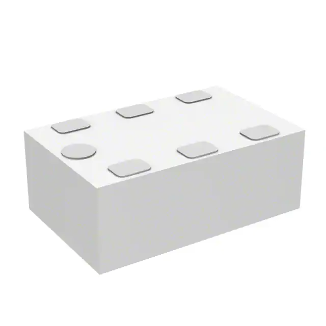
Ultra Low Profile 0805
3 dB, 90° Hybrid Coupler
Description
The C1517J5003AHF is a low cost, low profile sub-miniature high
performance 3 dB coupler in an easy to use surface mount package. The
C1517J5003AHF is ideal for balanced power and low noise amplifiers, plus signal
distribution and other applications where low insertion loss and tight amplitude and
phase balance are required. The C1517J5003AHF is available on tape and reel for
pick and place high volume manufacturing.
All of the Xinger components are constructed from ceramic filled PTFE
composites which possess excellent electrical and mechanical stability. All parts
have been subjected to rigorous qualification testing and units are 100% RF tested.
Detailed Electrical Specifications: Specifications subject to change without notice.
ROOM (25°°C)
Features:
•
•
•
•
•
•
•
•
•
•
•
1500 – 1700 MHz
0.7mm Height Profile
High Isolation & Low Loss
LTE Bands: 24
Surface Mountable
Tape & Reel
Non-conductive Surface
RoHS Compliant
Halogen-Free
100% RF Tested
-55°C to 85°C
Parameter
Min.
Frequency
1500
Port Impedance
Return Loss
Isolation
Insertion Loss*
Amplitude Balance
Phase Balance (relative to 90°)
50
25
28
0.2
0.4
0.7
21
24
Power Handling
Operating Temperature
Group Delay
(1.5-1.7GHZ)
(nSec)
Typ.
-55
Max
Unit
1700
MHz
0.3
1.0
4
Ω
dB
dB
dB
dB
Degrees
4
+85
Watts
ºC
Min.
Typ.
Max
0.093
0.108
0.123
* Insertion Loss stated at room temperature (Insertion Loss is approximately 0.1 dB higher at +85 ºC)
Outline Drawing
Top View (Nearside)
2.04±0.10
Bottom View (Farside)
Side View
4x 0.37
0.70±0.07
1
2
3
2x 0.15
1.29±0.10
6x 0.98
6x 0.22
Orientation Marker
Denotes Pin Location
Orientation Marker
Denotes Pin Location
6
5
4
4x 0.65
6x 0.30
Pin
1
2
3
4
5
6
Configuration-1
Input
GND
Isolated
Direct
GND
Coupled
Configuration-2
Isolated
GND
Input
Coupled
GND
Direct
Configuration-3
Direct
GND
Coupled
Input
GND
Isolated
Configuration-4
Coupled
GND
Direct
Isolated
GND
Input
Visit us at
www.anaren.com
Mechanical Outline
-Dimensions are in Millimeters
-Tolerances are Non-Cumulative
USA/Canada:
Toll Free:
Europe:
Asia:
(315) 432-8909
(800) 411-6596
+44 2392-232392
+86 512-62749282
�Model C1517J5003AHF
Rev D
Typical Broadband Performance: 500 MHz. to 6000 MHz.
Insertion Loss (dB)
0
-5
-0.5
-10
-1
Insertion Loss (dB)
Return Loss at Input Port (dB)
Return Loss at Input Port (dB)
0
-15
-20
-1.5
-2
-25
-2.5
-30
-3
-35
0.5
-3.5
1
1.5
2
2.5
3
3.5
Freq [GHz]
4
4.5
5
5.5
6
0.5
1
1.5
2
20
1.5
15
1
10
0.5
0
-0.5
-15
2
2.5
3
3.5
Freq [GHz]
5
5.5
6
4.5
5
5.5
6
-5
-1.5
1.5
4.5
0
-10
1
4
5
-1
-2
0.5
3
3.5
Freq [GHz]
Phase balance(degree)
2
Phase balance(degree)
Amplitude Balance (dB)
Amplitude Balance (dB)
2.5
4
4.5
5
5.5
6
4
4.5
5
5.5
6
-20
0.5
1
1.5
2
2.5
3
3.5
Freq [GHz]
4
Isolation (dB)
0
-5
Isolation (dB)
-10
-15
-20
-25
-30
-35
0.5
1
1.5
2
2.5
3
3.5
Freq [GHz]
Visit us at
www.anaren.com
USA/Canada:
Toll Free:
Europe:
Asia:
(315) 432-8909
(800) 411-6596
+44 2392-232392
+86 512-62749282
�Model C1517J5003AHF
Rev D
Typical Performance: 1400 MHz. to 1800 MHz.
Insertion Loss (dB)
Return Loss at Input Port (dB)
0
-5
-0.5
-10
-1
Insertion Loss (dB)
Return Loss at Input Port (dB)
0
-15
-20
-1.5
-2
-25
-2.5
-30
-3
-35
1.4
-3.5
1.45
1.5
1.55
1.6
1.65
Freq [GHz]
1.7
1.75
1.8
1.4
1.45
1.5
1.55
1.6
1.65
Freq [GHz]
1.7
1.75
1.8
1.7
1.75
1.8
Phase balance(degree)
Amplitude Balance (dB)
10
2
8
1.5
6
Phase balance(degree)
Amplitude Balance (dB)
1
0.5
0
-0.5
4
2
0
-2
-4
-1
-6
-1.5
-8
-2
1.4
1.45
1.5
1.55
1.6
1.65
Freq [GHz]
1.7
1.75
1.8
1.7
1.75
1.8
-10
1.4
1.45
1.5
1.55
1.6
1.65
Freq [GHz]
Isolation (dB)
0
-5
Isolation (dB)
-10
-15
-20
-25
-30
-35
1.4
1.45
1.5
1.55
1.6
1.65
Freq [GHz]
Visit us at
www.anaren.com
USA/Canada:
Toll Free:
Europe:
Asia:
(315) 432-8909
(800) 411-6596
+44 2392-232392
+86 512-62749282
�Model C1517J5003AHF
Rev D
Definition of Measured Specifications
Parameter
Return Loss
Isolation
Insertion Loss
Definition
Mathematical Representation
i, j, k, m is denoted as the port index of input, isolated, direct
and coupled port for specific pin configuration shown in the table
The impedance match of the
coupler to a 50Ω system. Return
Loss is an alternate means to
express VSWR.
The input power divided by the
sum of the power at the two
output ports.
The input power divided by the
sum of the power at the two
output ports.
Amplitude
Balance
The difference in power between
the two outputs.
Phase Balance
The difference in phase angle
between the two output ports.
Group Delay
Group delay is defined as the
average of the mean group delay
of the coupling path and the
mean group delay of the direct
path.
20 log10 ( Sii )
20log10 S ji
2
2
10 log10 ( S mi + S ki )
20log10 (
Ski
)
Smi
∠S ki − ∠S mi + 90 o
Group delay (ns) =
Mean ( GD ( Smi ) ) + Mean ( GD ( S ki ) )
2
where " Mean " is the arithmetic mean of the group
delay over a frequency band.
*100% RF test is performed per spec definition for pin configuration 1 and port 1 (input port) is connected to pin1, port 2 (isolated port) is connected to
pin 3, port 3 (direct port) is connected to pin 4 and port 4 (isolated) is connected to pin 6.
Visit us at
www.anaren.com
USA/Canada:
Toll Free:
Europe:
Asia:
(315) 432-8909
(800) 411-6596
+44 2392-232392
+86 512-62749282
�Model C1517J5003AHF
Rev D
Mounting Configuration:
In order for Xinger surface mount components to work optimally, the proper impedance transmission lines must be
used to connect to the RF ports. If this condition is not satisfied, insertion loss, Isolation and VSWR may not meet
published specifications.
All of the Xinger components are constructed from organic PTFE based composites which possess excellent
electrical and mechanical stability. Xinger components are compliant to a variety of ROHS and Green standards and
ready for Pb-free soldering processes. Pads are Gold plated with a Nickel barrier.
An example of the PCB footprint used in the testing of these parts is shown below. In specific designs, the
transmission line widths need to be adjusted to the unique dielectric coefficients and thicknesses as well as varying
pick and place equipment tolerances.
6x 0.35
4x 0.30
6x 0.33
0.66
6x 0.05
4x Transmission
Line
Plated thru
holes to
ground
Circuit Pattern
Footprint Pad (s)
Solder Resist
Dimensions are in Millimeters
Mounting Footprint
Visit us at
www.anaren.com
USA/Canada:
Toll Free:
Europe:
Asia:
(315) 432-8909
(800) 411-6596
+44 2392-232392
+86 512-62749282
�Model C1517J5003AHF
Rev D
Packaging and Ordering Information
Parts are available in reel and are packaged per EIA 481-2. Parts are oriented in tape and reel as shown below.
Minimum order quantities are 4000 per reel. See Model Numbers below for further ordering information.
2.00
.81
4.00
1.75
3.50
8.00
1.60
4.00
2.41
.25
Visit us at
www.anaren.com
USA/Canada:
Toll Free:
Europe:
Asia:
(315) 432-8909
(800) 411-6596
+44 2392-232392
+86 512-62749282
�
很抱歉,暂时无法提供与“C1517J5003AHF”相匹配的价格&库存,您可以联系我们找货
免费人工找货