PD1722J5050D2HF
Rev D
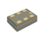
Ultra Low Profile 0805 Power Divider
50Ω to 50Ω
Description:
The PD1722J5050D2HF is a low profile, sub-miniature Wilkinson power
divider in an easy to use surface mount package. The PD1722J5050D2HF
is ideal for high volume manufacturing and delivers higher performances than
traditional printed and lumped element solutions. The PD1722J5050D2HF
is matched to 50 Ω and has a height profile of 0.5 mm which is ideal for high
level integrations in the following markets: WCDMA, and GSM, The
PD1722J5050D2HF does not include the resistive element and therefore,
requires an external resistor for operation. The PD1722J5050D2HF is
available on tape and reel for high volume manufacturing pick and place.
Detailed Electrical Specifications:
Specifications subject to change without notice.
Features:
•
•
•
•
•
•
•
•
•
•
•
1700-2200 MHz
19 dB Isolation (output ports)
0.5mm Height Profile
50Ω Input / 50Ω Outputs
Low Insertion Loss
Surface Mountable
Tape & Reel
Non-conductive Surface
RoHS Compliant
External resistors required
Halogen Free
ROOM (25°C)
Parameter
Min.
Frequency
Input Port Impedance
Output Port Impedance
Return Loss
Insertion Loss*
Amplitude Balance
Phase Balance
Isolation (Output Ports)
Power Handling @85oC
Operating Temperature
1700
Typ.
50
50
14
0.5
0.1
1
19
11
17
Max
Unit
2200
MHz
Ω
Ω
dB
dB
dB
Degrees
dB
Watts
ºC
0.7
0.3
3
2
+140
-55
*Insertion Loss stated at room temperature (Insertion Loss is approximately 0.1 dB higher at +85 ºC)
Outline Drawing:
TOP VIEW (Near Side)
2.04±0.10
SIDE VIEW
BOTTOM VIEW (Far Side)
4x 0.37
0.85±0.08
3
2
1
2x 0.15
1.29±0.10
6x 0.98
Orientation Marker
Denotes Pin Location
Orientation Marker
Denotes Pin Location
Mechanical Outline
-Dimensions are in Millimeters
Pin
1
2
3
4
5
6
6x
0.22
6
4x 0.65
5
4
6x
0.30
Designation
Output 1
Input
Mid 2
Mid 1
GND
Output 2
1
�PD1722J5050D2HF
Rev D
Typical Performance: 500 MHz. to 6.0 GHz.
Insertion Loss
0
-3
-3
-6
-6
-9
-9
-12
-12
-15
-15
[dB]
-18
-18
-21
-21
-24
-24
-27
-27
-30
-30
-33
-33
1.5
15
1
10
0.5
5
Isolation
0
-3
-6
-9
-12
-15
-18
-21
-24
-27
-30
-33
8000
7500
7000
6500
6000
5500
5000
4500
4000
3500
3000
2500
2000
1500
500
-36
1000
[dB]
8000
7500
7000
6500
6000
5500
Frequency [MHz]
Frequency [MHz]
Frequency [MHz]
2
8000
7500
7000
6500
6000
5500
5000
4500
4000
3500
3000
2500
2000
8000
7500
7000
6500
6000
5500
5000
4500
4000
3500
-20
3000
-15
-2
2500
-1.5
2000
-10
1500
-1
1500
0
-5
1000
0
-0.5
500
deg
2
20
1000
5000
Phase Balance
Amplitude Balance
500
4500
Frequency [MHz]
Frequency [MHz]
[dB]
4000
3500
3000
2500
2000
500
8000
7500
7000
6500
6000
5500
5000
4500
4000
3500
3000
2500
2000
1500
1000
500
1500
-36
-36
1000
[dB]
Return Loss - Input
0
�PD1722J5050D2HF
Rev D
Wide Band Performance: 1600 MHz. to 2300 MHz.
Return Loss - Input
Insertion Loss
0.0
-3
-0.3
-6
-0.6
-9
-0.9
-12
-1.2
-15
-1.5
Amplitude Balance
1.5
15
1
10
0.5
5
Frequency [MHz]
2300
2300
2200
2100
2300
2200
-20
2100
-2
2000
-15
1900
-10
1800
-1
-1.5
2000
-5
1900
-0.5
1800
0
1700
0
1600
deg
20
1700
2200
Phase Balance
2
1600
2100
Frequency [MHz]
Frequency [MHz]
[dB]
2000
1600
2300
2200
2100
-3.6
2000
-3.3
-36
1900
-3.0
-33
1800
-2.7
-30
1700
-2.4
-27
1600
-2.1
-24
1900
-1.8
-21
1800
-18
1700
[dB]
[dB]
0
Frequency [MHz]
Isolation
0
-3
-6
-9
-15
-18
-21
-24
-27
-30
-33
2300
2200
2100
2000
1900
1800
1700
-36
1600
[dB]
-12
Frequency [MHz]
3
�PD1722J5050D2HF
Rev D
Mounting Configuration:
In order for Xinger surface mount components to work optimally, the proper impedance transmission lines must
be used to connect to the RF ports. If this condition is not satisfied, insertion loss, Isolation and VSWR may
not meet published specifications.
All of the Xinger components are constructed from organic PTFE based composites which possess excellent
electrical and mechanical stability. Xinger components are compliant to a variety of ROHS and Green
standards and ready for Pb-free soldering processes. Pads are Gold plated with Nickel barrier.
An example of the PCB footprint used in the testing of these parts is shown below. In specific designs, the
transmission line widths need to be adjusted to the uniue dielectric coefficients and thicknesses as well as
varying pick and place equipment tolerances. In addition, since the PD1722J5050D2HF is a Wilkinson power
divider, external 0402 100Ω and 200Ω resistors must be mounted in locations R1 and R2 respectively, as
shown in the Figure below.
Pad Footprint w/ 0402 Resistor Locations
3X Transmission
Line
6X .014
[0.35]
6X .013
[0.33]
R1
4X .012
[0.30]
.026
[0.66]
R2
Plated thru
hole to
ground
Circuit Pattern
Footprint Pad (s)
Solder Resist
Dimensions are in Inches [Millimeters]
Mounting Footprint
4
�PD1722J5050D2HF
Rev D
Packaging and Ordering Information:
Parts are available in reel and are packaged per EIA 481-2. Parts are oriented in tape and reel as shown
below. Minimum order quantities are 4000 per reel. See Model Numbers below for further ordering
information.
1.00
2.00
4.00
1.75
3.50
8.00
1.60
4.00
2.41
.25
Contact us:
rf&s_support@ttm.com
5
�
很抱歉,暂时无法提供与“PD1722J5050D2HF”相匹配的价格&库存,您可以联系我们找货
免费人工找货