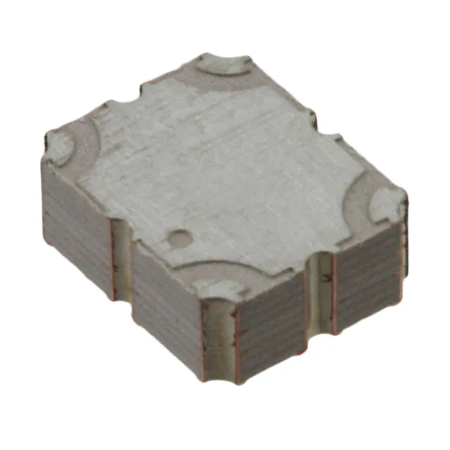
X3C19P2-30S
Rev F
30 dB Directional Coupler
Description:
The X3C19P2-30S is a low profile, high performance 30dB directional
coupler in a new easy to use, manufacturing friendly surface mount
package. It is designed for DCS, PCS, WCDMA and LTE band
applications. The X3C19P2-30S is designed particularly for power and
frequency detection, as well as for VSWR monitoring, where tightly
controlled coupling and low insertion loss is required. It can be used in
high power applications up to 200 Watts.
Parts have been subjected to rigorous qualification testing and they
are manufactured using materials with coefficients of thermal
expansion (CTE) compatible with common substrates such as FR4,
G-10, RF-35, RO4003 and polyimide. Produced with 6 of 6 RoHS
compliant tin immersion finish
Features:
• 1400 - 2700 MHz
• DCS, PCS, WCDMA and LTE
•
High Power
• Very Low Loss
• Tight Coupling
• High Directivity
• Production Friendly
• Tape and Reel
• Lead Free
Detailed Electrical Specifications:
Frequency
Mean
Coupling
Insertion
Loss
VSWR
MHz
dB
dB Max
Max : 1
1400 – 2700
1805 – 1880
1930 - 1990
2110 - 2170
30.4 ± 1.50
30.0 ± 1.50
30.0 ± 1.50
30.2 ± 1.50
0.10
0.075
0.075
0.10
1.33
1.12
1.12
1.21
Directivity
Frequency
Sensitivity
Power
Operating
Temp.
dB Min
dB Max
ºC
20
20
20
20
± 2.0
± 0.05
± 0.05
± 0.3
Avg. CW Watts
@95 ºC
200
200
200
200
-55 to +150
-55 to +150
-55 to +150
-55 to +150
**Specification based on performance of unit properly installed on TTM Technologies Test Board 61015-0001. Refer to Specifications
subject to change without notice. Refer to parameter definitions for details.
Outline Drawing:
1
�X3C19P2-30S
Rev F
Hybrid Coupler Pin Configuration
The X3C19P2-30S has an orientation marker to denote Pin 1. Once port one has been identified the other
ports are known automatically. Please see the chart below for clarification:
Pin 1
Input
Direct
Pin 2
Direct
Input
Pin 3
Isolated
Coupled
Pin 4
Coupled
Isolated
Note: The direct port has a DC connection to the input port and the coupled port has a DC connection to the
isolated port.
For optimum IL and power handling performance, use Pin 1 or Pin 2 as inputs.
Peak Power Handling
High-Pot testing of these couplers during the qualification procedure resulted in a minimum breakdown voltage
of 1.40 kV. This voltage level corresponds to a breakdown resistance capable of handling at least 12dB peaks
over average power levels, for very short durations. The breakdown location consistently occurred across the
air interface at the coupler contact pads (see illustration below). The breakdown levels at these points will be
affected by any contamination in the gap area around these pads. These areas must be kept clean for optimum
performance. It is recommended that the user test for voltage breakdown under the maximum operating
conditions and over worst case modulation induced power peaking. This evaluation should also include
extreme environmental conditions (such as high humidity).
2
�X3C19P2-30S
Rev F
Insertion Loss and Power Derating Curves
Typical Insertion Loss Derating Curve for X3C19P2-30
X3C19P2-30 Power Derating Curve
0
400
typical insertion loss (f=1880Mhz)
typical insertion loss (f=1990Mhz)
typical insertion loss (f=2170Mhz)
typical insertion loss (f=2600Mhz)
-0.01
1400 - 2700Mhz
300
Power (Watts)
Insertion Loss (dB)
-0.02
350
-0.03
-0.04
250
200
150
-0.05
100
-0.06
50
-0.07
-100
-50
0
50
100
150
200
o
Temperature of the Part ( C)
0
0
50
95
100
150
200
Mounting Interface Temperature (oC)
Insertion Loss Derating:
Power Derating:
The insertion loss, at a given frequency, of a group
of couplers is measured at 25°C and then averaged.
The measurements are performed under small
signal conditions (i.e. using a Vector Network
Analyzer). The process is repeated at 85°C and
150°C. A best-fit line for the measured data is
computed and then plotted from -55°C to 150°C.
The power handling and corresponding power
derating plots are a function of the thermal
resistance, mounting surface temperature (base
plate temperature), maximum continuous operating
temperature of the coupler, and the thermal insertion
loss. The thermal insertion loss is defined in the
Power Handling section of the data sheet.
As the mounting interface temperature approaches
the maximum continuous operating temperature, the
power handling decreases to zero.
If mounting temperature is greater than 95°C, Xinger
coupler will perform reliably as long as the input
power is derated to the curve above.
3
�X3C19P2-30S
Rev F
Typical Performance: (-55°C, 25°C, 95°C & 125°C): 1400-2700 MHz
0
Return Loss for X3C19P2-30S(Feeding port1)
0
-55C
25C
95C
125C
-10
-20
Return Loss (dB)
Return Loss (dB)
-55C
25C
95C
125C
-10
-20
-30
-40
-30
-40
-50
-50
-60
-60
-70
1400
Return Loss for X3C19P2-30S(Feeding port2)
1600
1800
2000
2200
Freq (MHz)
2400
2600
2800
-70
1400
1600
1800
2000
2200
Freq (MHz)
2400
2600
2800
4
�X3C19P2-30S
Rev F
Typical Performance: (-55°C, 25°C, 95°C & 125°C): 1400-2700 MHz
-28
Coupling for X3C19P2-30S(Feeding port1)
0
-55C
25C
95C
125C
-28.5
Directivity for X3C19P2-30S(Feeding port1)
-55C
25C
95C
125C
-10
-29
-20
Directivity (dB)
Coupling [dB]
-29.5
-30
-30
-30.5
-40
-31
-50
-31.5
-32
1400
0
1600
1800
2000
2200
Freq (MHz)
2400
2600
-60
1400
2800
Insertion Loss for X3C19P2-30S(Feeding port1)
0
-55C
25C
95C
125C
-0.02
-0.04
2000
2200
Freq (MHz)
2400
2600
2800
Transmission Loss for X3C19P2-30S(Feeding port1)
-55C
25C
95C
125C
-0.04
-0.06
Transmission Loss (dB)
Insertion Loss (dB)
1800
-0.02
-0.06
-0.08
-0.1
-0.12
-0.08
-0.1
-0.12
-0.14
-0.14
-0.16
-0.16
-0.18
-0.18
-0.2
1400
1600
1600
1800
2000
2200
Freq (MHz)
2400
2600
2800
-0.2
1400
1600
1800
2200
2000
Freq (MHz)
2400
2600
2800
5
�X3C19P2-30S
Rev F
Definition of Measured Specifications
Parameter
VSWR
(Voltage Standing Wave Ratio)
Return Loss
Mean Coupling
Insertion Loss
Definition
The impedance match of
the coupler to a 50Ω
system. A VSWR of 1:1 is
optimal.
The impedance match of
the coupler to a 50Ω
system. Return Loss is an
alternate means to express
VSWR.
At a given frequency (ωn),
coupling is the input power
divided by the power at the
coupled port. Mean
coupling is the average
value of the coupling values
in the band. N is the
number of frequencies in
the band.
The input power divided by
the sum of the power at the
two output ports.
Transmission Loss
The input power divided by
the power at the direct port.
Directivity
The power at the coupled
port divided by the power at
the isolated port.
Frequency Sensitivity
The decibel difference
between the maximum in
band coupling value and
the mean coupling, and the
decibel difference between
the minimum in band
coupling value and the
mean coupling.
Mathematical Representation
𝑉𝑉𝑚𝑚𝑚𝑚𝑚𝑚
𝑉𝑉𝑉𝑉𝑉𝑉𝑉𝑉 =
𝑉𝑉𝑚𝑚𝑚𝑚𝑚𝑚
Vmax = voltage maxima of a standing wave
Vmin = voltage minima of a standing wave
𝑅𝑅𝑅𝑅𝑅𝑅𝑅𝑅𝑅𝑅𝑅𝑅 𝐿𝐿𝐿𝐿𝐿𝐿𝐿𝐿(𝑑𝑑𝑑𝑑) = 20𝑙𝑙𝑙𝑙𝑙𝑙
𝑉𝑉𝑉𝑉𝑉𝑉𝑉𝑉 + 1
𝑉𝑉𝑉𝑉𝑉𝑉𝑉𝑉 − 1
𝐶𝐶𝐶𝐶𝐶𝐶𝐶𝐶𝐶𝐶𝐶𝐶𝐶𝐶𝐶𝐶(𝑑𝑑𝑑𝑑) = 𝐶𝐶(𝜔𝜔𝑛𝑛 ) = 10𝑙𝑙𝑙𝑙𝑙𝑙
𝑀𝑀𝑀𝑀𝑀𝑀𝑀𝑀 𝐶𝐶𝐶𝐶𝐶𝐶𝐶𝐶𝐶𝐶𝐶𝐶𝐶𝐶𝐶𝐶(𝑑𝑑𝑑𝑑) =
∑𝑁𝑁
𝑛𝑛=1 𝐶𝐶(𝜔𝜔𝑛𝑛 )
𝑁𝑁
𝐼𝐼𝐼𝐼𝐼𝐼𝐼𝐼𝐼𝐼𝐼𝐼𝐼𝐼𝐼𝐼𝐼𝐼 𝐿𝐿𝐿𝐿𝐿𝐿𝐿𝐿(𝑑𝑑𝑑𝑑) = 10𝑙𝑙𝑙𝑙𝑙𝑙
10𝑙𝑙𝑙𝑙𝑙𝑙
𝑃𝑃𝑖𝑖𝑖𝑖
𝑃𝑃𝑑𝑑𝑑𝑑𝑑𝑑𝑑𝑑𝑑𝑑𝑑𝑑
10𝑙𝑙𝑙𝑙𝑙𝑙
𝑃𝑃𝑖𝑖𝑖𝑖 (𝜔𝜔𝑛𝑛 )
𝑃𝑃𝑐𝑐𝑐𝑐𝑐𝑐 (𝜔𝜔𝑛𝑛 )
𝑃𝑃𝑖𝑖𝑖𝑖
𝑃𝑃𝑐𝑐𝑐𝑐𝑐𝑐 + 𝑃𝑃𝑑𝑑𝑑𝑑𝑑𝑑𝑑𝑑𝑑𝑑𝑑𝑑
𝑃𝑃𝑐𝑐𝑐𝑐𝑐𝑐
𝑃𝑃𝑖𝑖𝑖𝑖𝑖𝑖
Max Coupling (dB) – Mean Coupling (dB)
and
Min Coupling (dB) – Mean Coupling (dB)
6
�X3C19P2-30S
Rev F
Packaging and Ordering Information
Parts are available in reels. Packaging follows EIA 481-2 for reels. Parts are oriented in tape and reel as
shown below. Minimum order quantities are 2000 per reel.
.157
[4.00]
.012
[0.30]
.217
[5.50]
TYP Ø.059
[Ø1.50]
.315
[8.00]
.079
[2.00]
.217
[5.50] .472
[12.00]
RR
.264
[6.70]
.069
[1.75]
MODEL
NO
CC
.079
[2.00]
Dimensions are in Inches [Millimeters]
Direction Of
Part Feed
(Unloading)
Contact us:
rf&s_support@ttm.com
7
�
很抱歉,暂时无法提供与“X3C19P2-30S”相匹配的价格&库存,您可以联系我们找货
免费人工找货