APW8805
3A 5V 1MHz Synchronous Buck Converter
Features
General Description
•
High Efficiency up to 95%
APW8805 is a 3A synchronous buck converter with inte-
•
Adjustable Output Voltage from 0.8V to VVIN
grated 75mΩ high side and 55mΩ low side power
MOSFETs. The APW8805, design with a current-mode
•
Integrated 75mΩ High Side / 55mΩ Low Side
control scheme, can convert wide input voltage of 2.6V to
6V to the output voltage adjustable from 0.8V to 6V to
MOSFETs
•
Low Dropout Operation: 100% Duty Cycle
•
Mode Selection
provide excellent output voltage regulation.
The APW8805 is equipped with an automatic PFM/PWM
- APW8805 : PFM/PWM mode
•
Stable with Low ESR Ceramic Capacitors
•
Power-On-Reset Detection on VCC and VIN
•
Integrated Soft-Start and Soft-Stop
•
Over-Temperature Protection
•
Over-Voltage Protection
•
Under-Voltage Protection
•
High/ Low Side Current Limit
•
Power Good Indication
•
Enable/Shutdown Function
•
Current-Mode Operation with Internal
•
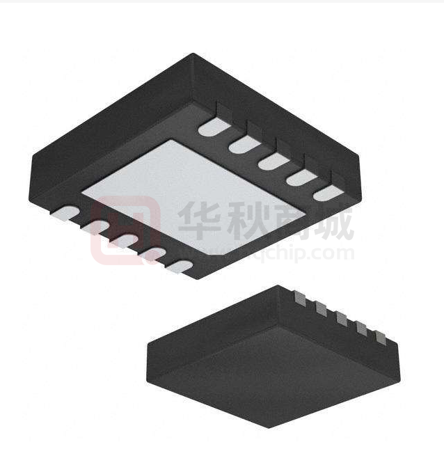
Small TDFN3x3-10 Packages
•
Lead Free and Green Devices Available
mode operation. At light load , the IC operates in the PFM
mode to reduce the switching losses. At heavy load, the
IC works in PWM mode. At PWM mode, the switching
frequency is set by the external resistor.
The APW8805 is also equipped with Power-on-reset, softstart, soft-stop, and whole protections (under-voltage,
over-voltage, over-temperature and current-limit) into a
single package.
This device, available TDFN3x3-10, provides a very compact system solution external components and PCB area.
Compensation
Simplified Application Circuit
(RoHS Compliant)
Applications
•
•
Notebook Computer & UMPC
•
Set-Top Box
•
DSL, Switch HUB
•
VIN
VOUT
VIN
SW
VCC
FB
LCD Monitor/TV
(option)
APW8805
POK
ON
OFF
Portable Instrument
GND
EN
ANPEC reserves the right to make changes to improve reliability or manufacturability without notice, and
advise customers to obtain the latest version of relevant information to verify before placing orders.
Copyright ANPEC Electronics Corp.
Rev. A.4 - Apr., 2016
1
www.anpec.com.tw
�APW8805
Ordering and Marking Information
APW8805
Assembly Material
Handling Code
Temperature Range
Package Code
APW8805 QB :
Package Code
QB : TDFN3x3-10
Operating Ambient Temperature Range
I : -40 to 85 oC
Handling Code
TR : Tape & Reel
Assembly Material
G : Halogen and Lead Free Device
APW
8805
XXXXX
XXXXX - Date Code
Note: ANPEC lead-free products contain molding compounds/die attach materials and 100% matte tin plate termination finish; which
are fully compliant with RoHS. ANPEC lead-free products meet or exceed the lead-free requirements of IPC/JEDEC J-STD-020D for
MSL classification at lead-free peak reflow temperature. ANPEC defines “Green” to mean lead-free (RoHS compliant) and halogen
free (Br or Cl does not exceed 900ppm by weight in homogeneous material and total of Br and Cl does not exceed 1500ppm by
weight).
Pin Configuration
APW8805
FB 1
VCC 2
VIN 3
GND 4
GND 5
10 EN
9 POK
8 NC
7 SW
6 SW
11
GND
TDFN 3X3-10
(Top View)
11
GND Exposed pad
Absolute Maximum Ratings (Note 1)
S ymbol
V VIN , VVCC
Pa ramete r
In put S uppl y Volta ge
Rating
Unit
-0.3 ~ 6.5
V
-2V~7 .5V
-0 .3V ~6 .5V
V
-0.3 ~ 6.5
V
SW to GND Volta ge
10n s pu lse width
POK, FB, EN to G ND Voltage
PD
Power Dissipation
Interna lly Limi ted
W
TJ
Ju nctio n Temp erature
15 0
o
T STG
Sto rage Temperature
-65 ~ 1 50
o
C
T SDR
Ma xim um Le ad So lderin g Tempe ratu re, 1 0 S econd s
26 0
o
C
C
Note1: Stresses beyond those listed under "absolute maximum ratings" may cause permanent damage to the device. These are
stress ratings only and functional operation of the device at these or any other conditions beyond those indicated under "recommended operating conditions" is not implied. Exposure to absolute maximum rating conditions for extended periods may affect device
reliability.
Copyright ANPEC Electronics Corp.
Rev. A.4 - Apr., 2016
2
www.anpec.com.tw
�APW8805
Thermal Characteristics
Symbol
Parameter
θJA
Junction-to-Ambient Resistance in Free Air
θJC
Junction-to-Case Resistance in Free Air
Typical Value
Unit
(Note 2)
TDFN3x3-10
50
TDFN3x3-10
10
o
C/W
o
C/W
(Note 3)
Note 2: θJA is measured with the component mounted on a high effective thermal conductivity test board in free air. The exposed pad
of SOP-8P or TDFN3x3-10 is soldered directly on the PCB.
Note 3: The case temperature is measured at the center of the exposed pad on the underside of the SOP-8P or TDFN3x3-10 package.
Recommended Operating Conditions (Note 4)
Symbol
Parameter
Range
Unit
2.6~ 6
V
2~6
V
VVCC
Control and Driver Supply Voltage
VVIN
Input Supply Voltage
VOUT
Converter Output Voltage
0.8~6
V
Inductance
1~2.2
µH
L
IOUT
Converter Output Current
0~3
A
TA
Ambient Temperature
-40 ~ 85
o
TJ
Junction Temperature
-40 ~ 125
o
C
C
Note 4: Refer to the typical application circuit.
Electrical Characteristics
Unless otherwise specified, these specifications apply over VVCC=VVIN=5V, VOUT=3.3V, TA=25oC.
Symbo
Parameter
APW8805
Test Conditions
Unit
Min.
Typ.
Max.
SUPPLY CURRENT
VCC Supply Current
VFB=0.7V
-
460
-
µA
IVCC_SDH VCC Shutdown Supply Current
EN=GND
-
-
1
µA
2.3
2.4
2.5
V
IVCC
POWER-ON-RESET (POR)
VCC POR Voltage Threshold
VVCC Rising
VCC POR Hysteresis
VIN POR Voltage Threshold
VIN POR Hysteresis
-
0.2
-
V
1.5
1.7
1.9
V
-
0.2
-
V
-
0.8
-
V
-1
-
+1
%
-1.5
-
+1.5
%
REFERENCE VOLTAGE
VREF
Reference Voltage
All temperature
Output Accuracy
Copyright ANPEC Electronics Corp.
Rev. A.4 - Apr., 2016
IOUT=10mA~3A, VVCC=2.6~5V
3
www.anpec.com.tw
�APW8805
Electrical Characteristics (Cont.)
Unless otherwise specified, these specifications apply over VVCC=VVIN=5V, VOUT=3.3V, TA=25oC.
Symbo
Parameter
APW8805
Test Conditions
Unit
Min.
Typ.
Max.
0.85
1
1.15
MHz
-
100
-
%
-
100
-
ns
-
75
90
mΩ
-
55
75
mΩ
-
-
10
µA
-
550
-
µA/V
OSCILLATOR AND DUTY CYCLE
FOSC
Oscillator Frequency
Maximum Converter’s Duty
VFB=0.7V
Minimum on Time
POWER MOSFET
High Side P-MOSFET Resistance
Low Side N-MOSFET Resistance
VVCC=5V, ISW =0.5A, TA=25oC
o
VVCC=5V, ISW =0.5A, TA=25 C
High/Low Side MOSFET Leakage
Current
CURRENT-MODE PWM CONVERTER
Gm
Error Amplifier Transconductance
Error Amplifier DC Gain
TD
-
80
-
dB
Current Sense Transresistance
COMP=NC
-
400
-
mΩ
Dead Time
-
20
-
ns
4
5
6
A
-
160
-
°C
PROTECTIONS
ILIM
High Side MOSFET Current-Limit
TOTP
Over-Temperature Trip Point
Peak Current
-
50
-
°C
Over-Voltage Protection Threshold
120
-
135
%VREF
Under-Voltage Protection Threshold
45
50
55
%VREF
Soft-Start Time
-
1
-
ms
EN Enable Threshold
-
-
1.4
V
0.5
-
-
V
87
90
93
%VOUT
POK Low Hysteresis
(POK Goes Low)
-
5
-
%VOUT
POK in from Higher
(POK Goes High)
122
125
128
%VOUT
-
5
-
%VOUT
-
100
-
Ω
Over-Temperature Hysteresis
SOFT-START, ENABLE, AND INPUT CURRENTS
EN Shutdown Threshold
POK in from Lower
(POK Goes High)
POK Threshold
POK High Hysteresis
(POK Goes Low)
Power Good Pull Low Resistance
Copyright ANPEC Electronics Corp.
Rev. A.4 - Apr., 2016
4
www.anpec.com.tw
�APW8805
Typical Operating Characteristics
Refer to the “Typical Application Circuit”. The test condition is VVCC=VVIN=5V, TA= 25oC unless otherwise specified.
Efficiency vs. Load Current
100
90
90
Efficiency (%)
Efficiency (%)
Efficiency vs. Load Current
100
80
VVCC=5V
70
80
70
VVIN=5V
V VIN=3.3V
60
60
V OUT=1.8V
VOUT=3.3V
50
50
0
1
2
Load Current, IOUT(A)
0
3
1
2
Load Current, IOUT(A)
3
Output Voltage vs. Load Current
Efficiency vs. Load Current
1.9
100
1.88
Output Voltage, VOUT(V)
Efficiency (%)
90
80
70
VVIN=5V
VVIN=3.3V
60
VOUT=1.05V
1.86
1.84
1.82
1.8
1.78
1.76
1.74
1.72
50
0
1
2
Load Current, IOUT(A)
1.7
3
0
1
1.5
2
Load Current, IOUT(A)
2.5
3
Supply Voltage vs. MOSFET On
Supply Voltage vs. P-FET Current
Limit
Resistance
100
MOSFET On Resistance, RON(mΩ)
6
P-FET Current Limit, ILIM(A)
0.5
5
4
3
2
1
90
80
70
60
50
40
P-FET
30
N-FET
20
10
0
0
2
3
4
5
Supply Voltage, VVIN(V)
Copyright ANPEC Electronics Corp.
Rev. A.4 - Apr., 2016
2
6
5
3
4
5
Supply Voltage, VVIN(V)
6
www.anpec.com.tw
�APW8805
Operating Waveforms
Refer to the typical application circuit. The test condition is VIN=5V, TA= 25oC unless otherwise specified.
Shutdown
Enable without Loading
1
VEN
VEN
1
2
2
VPOK , 5V/Div
VPOK , 5V/Div
VOUT , 1V/Div, DC
3
3
4
VOUT , 1V/Div, DC
4
IL , 1A/Div
IL , 1A/Div
TIME: 200µs/Div
TIME: 200µs/Div
Enable with 1.8A Loading
1
Shutdown
VEN
VEN
VPOK , 5V/Div
1
2
2
VPOK , 5V/Div
VOUT , 1V/Div, DC
VOUT , 1V/Div, DC
3
3
IL , 1A/Div
4
4
IL , 1A/Div
TIME: 200µs/Div
Copyright ANPEC Electronics Corp.
Rev. A.4 - Apr., 2016
TIME: 200µs/Div
6
www.anpec.com.tw
�APW8805
Operating Waveforms
Refer to the typical application circuit. The test condition is VIN=5V, TA= 25oC unless otherwise specified.
Load Transient Response
Load Transient Response
1.5A
2.5A
1A
IOUT , 1A/Div
10mA
IOUT , 1A/Div
1
1
2
2
VOUT , 100mV/Div, AC
VOUT , 100mV/Div, AC
TIME: 20µs/Div
TIME: 50µs/Div
Over Voltage Protection
Normal Operating Waveform
V SW , 5V/Div
1
VPOK , 5V/Div
1
V OUT , 20mV/Div, DC
VOUT , 1V/Div, DC
2
2
3
IL , 1A/Div
IL , 1A/Div
3
TIME: 1µs/Div
TIME: 20µs/Div
Copyright ANPEC Electronics Corp.
Rev. A.4 - Apr., 2016
7
www.anpec.com.tw
�APW8805
Pin Description
NO.
NAME
FUNCTION
1
FB
Output Feedback Input. The APW8805 senses the feedback voltage via FB and regulates the
voltage at 0.8V. Connecting FB with a resistor-divider from the converter’s output sets the
output voltage.
2
VCC
Signal Input. VCC supplies the control circuitry, gate drivers. Connecting a ceramic bypass
capacitor from VCC to GND to eliminate switching noise and voltage ripple on the input to the
IC.
3
VIN
Power Input. VIN supplies the step-down converter switches. Connecting a ceramic bypass
capacitor from VIN to GND to eliminate switching noise and voltage ripple on the input to the
IC.
4,5
GND
Ground. Power and signal ground.
6,7
SW
Power Switching Output. SW is the Junction of the high-side and low-side Power MOSFETs
to supply power to the output LC filter.
8
NC
No connection.
9
POK
Power Good Output. This pin is open-drain logic output that is pulled to the ground when the
output voltage is out of regulation point.
10
EN
Enable Input. EN is a digital input that turns the regulator on or off. Drive EN high to turn on
the regulator, drive it low to turn it off.
11
GND
Ground and Exposed pad. Connect the exposed pad to the system ground plan with large
(Exposed Pad) copper area for dissipating heat into the ambient air.
Copyright ANPEC Electronics Corp.
Rev. A.4 - Apr., 2016
8
www.anpec.com.tw
�APW8805
Block Diagram
VIN
VCC
Current
Sense
Amplifier
LOC
Over
Temperature
Protection
PowerOnReset
Current
Limit
Zero Crossing
Comparator
POR
125%V REF
OTP
OVP
Fault
Logics
50%VREF
UVP
Inhibit
125%V REF
Gate
Control
SW
POK
90%VREF
Current
Compartor
Error
Amplifier
FB
Gate
Driver
Gat
e
Gm
Soft-start
V REF
0.8V
Slope
Compensation
Oscillator
Shutdown
EN
LOC
Current
Sense
Amplifier
GND
POK
Copyright ANPEC Electronics Corp.
Rev. A.4 - Apr., 2016
9
www.anpec.com.tw
�APW8805
Typical Application Circuit
L1
1.5µH
VIN
VIN
R3
100k
CIN
22µF
SW
C1
(option)
VCC
APW8805
COUT
22µFx2
R2
15k
GND
ON
Copyright ANPEC Electronics Corp.
Rev. A.4 - Apr., 2016
R1
4.7k
FB
POK
OFF
VOUT
1.05V/3A
EN
10
www.anpec.com.tw
�APW8805
Function Description
VCC and VIN Power-On-Reset (POR)
with a 50 oC hysteresis to lower the average TJ during
The APW8805 keeps monitoring the voltage on VCC and
VIN pins to prevent wrong logic operations which may
continuous thermal overload conditions, increasing lifetime of the APW8805.
occur when VCC or VIN voltage is not high enough for
internal control circuitry to operate. The VCC POR rising
Current-Limit Protection
The APW8805 monitors the output current, flows through
the high-side and low-side power MOSFETs, and limits
threshold is 2.4V (typical) with 0.2V hysteresis and VIN
POR rising threshold is 1.7V with 0.2V hysteresis.
the current peak at current-limit level to prevent the IC
from damaging during overload, short-circuit and over-
During start-up, the VCC and VIN voltage must exceed
the enable voltage threshold. Then, the IC starts a start-
voltage conditions. Typical high side power MOSFET current limit is 5A.
up process and ramps up the output voltage to the voltage target.
Output Under-Voltage Protection (UVP)
Soft-Start
In the operational process, if a short-circuit occurs, the
output voltage will drop quickly. Before the current-limit
circuit responds, the output voltage will fall out of the re-
The APW8805 has a built-in soft-start to control the rise
rate of the output voltage and limit the input current surge
quired regulation range. The under-voltage continually
monitors the FB voltage after soft-start is completed. If a
during start-up. During soft-start, an internal voltage ramp
connected to one of the positive inputs of the error
load step is strong enough to pull the output voltage lower
than the under-voltage threshold, the IC starts soft-stop
amplifier, rises up to replace the reference voltage (0.8V)
until the voltage ramp reaches the reference voltage. Dur-
function and shuts down converter’s output.
ing soft-start without output over-voltage, the APW8805
converter’s sinking capability is disabled until the output
The under-voltage threshold is 50% of the nominal output voltage. The under-voltage comparator has a built-in
voltage reaches the voltage target.
3µs noise filter to prevent the chips from wrong UVP shutdown being caused by noise. APW8805 will be latched
Soft-Stop
after under-voltage protection.
At the moment of shutdown controlled by EN signal, under-voltage event or over-voltage event, the APW8805 ini-
Over-Voltage Protection (OVP)
tiates a soft-stop process to discharge the output voltage
in the output capacitors. Certainly, the load current also
The over-voltage function monitors the output voltage by
discharges the output voltage. During soft-stop, the internal voltage ramp (VRAMP) falls down to replace the refer-
FB pin. When the FB voltage increases over 125% of the
reference voltage due to the high-side MOSFET failure or
ence voltage. Therefore, the output voltage falls down
slowly at the light load. After the soft-stop interval elapses,
for other reasons, the over-voltage protection comparator
will trigger soft-stop function and shutdown the converter
the soft-stop process ends and the IC turns.
output.
Over-Temperature Protection (OTP)
The over-temperature circuit limits the junction temperature of the APW8805. When the junction temperature ex-
Enable and Shutdown
Driving EN to ground places the APW8805 in shutdown.
ceeds TJ=+160 oC, a thermal sensor turns off the both
power MOSFETs, allowing the devices to cool. The ther-
In shutdown mode, the internal N-Channel power
MOSFET turns off, all internal circuitry shuts down and
mal sensor allows the converters to start a start-up process and to regulate the output voltage again after the
the quiescent supply current reduces to less than 1µA.
junction temperature cools by 50oC. The OTP is designed
Copyright ANPEC Electronics Corp.
Rev. A.4 - Apr., 2016
11
www.anpec.com.tw
�APW8805
Function Description (Cont.)
Powr Good Indicator
POK is actively held low in shutdown and soft-start status.
In the soft-start process, the POK is an open-drain. When
the soft-start is finished, the POK is released. In normal
operation, the POK window is from 90% to 125% of the
converter reference voltage. When the output voltage has
to stay within this window, POK signal will become high.
When the output voltage outruns 90% or 125% of the
target voltage, POK signal will be pulled low immediately.
In order to prevent false POK drop, capacitors need to
parallel at the output to confine the voltage deviation with
severe load step transient.
Copyright ANPEC Electronics Corp.
Rev. A.4 - Apr., 2016
12
www.anpec.com.tw
�APW8805
Application Information
shown in “Typical Application Circuits”. A suggestion of
maximum value of R2 is 20kΩ to keep the minimum cur-
Input Capacitor Selection
Because buck converters have a pulsating input current,
a low ESR input capacitor is required. This results in the
rent that provides enough noise rejection ability through
the resistor divider. The output voltage can be calculated
best input voltage filtering, minimizing the interference
with other circuits caused by high input voltage spikes.
as below:
R1
R1
VOUT = VREF ⋅ 1+
= 0.8 ⋅ 1 +
R2
R2
Also, the input capacitor must be sufficiently large to stabilize the input voltage during heavy load transients. For
good input voltage filtering, usually a 22µF input capacitor
is sufficient. It can be increased without any limit for better
VOUT
input-voltage filtering. Ceramic capacitors show better
performance because of the low ESR value, and they are
R1≤80Ω
less sensitive against voltage transients and spikes compared to tantalum capacitors. Place the input capacitor as
FB
R2 ≤ 20kΩ
APW8805
close as possible to the input and GND pin of the device
for better performance.
GND
Inductor Selection
Output Capacitor Selection
For high efficiencies, the inductor should have a low DC
The current-mode control scheme of the APW8805 allows the use of tiny ceramic capacitors. The higher ca-
resistance to minimize conduction losses. Especially at
high-switching frequencies, the core material has a
pacitor value provides the good load transients response.
Ceramic capacitors with low ESR values have the lowest
higher impact on efficiency. When using small chip
inductors, the efficiency is reduced mainly due to higher
output voltage ripple and are recommended. If required,
tantalum capacitors may be used as well. The output
inductor core losses. This needs to be considered when
selecting the appropriate inductor. The inductor value de-
ripple is the sum of the voltages across the ESR and the
ideal output capacitor.
termines the inductor ripple current. The larger the inductor value, the smaller the inductor ripple current and the
lower the conduction losses of the converter. Conversely,
larger inductor values cause a slower load transient
∆VOUT
response. A reasonable starting point for setting ripple
current, ∆IL, is 40% of maximum output current. The rec-
V
VOUT ⋅ 1 − OUT
VIN
≅
FSW ⋅ L
1
⋅ ESR +
8 ⋅ FSW ⋅ COUT
When choosing the input and output ceramic capacitors,
choose the X5R or X7R dielectric formulations. These
ommended inductor value can be calculated as below:
dielectrics have the best temperature and voltage characteristics of all the ceramics for a given value and size.
V
VOUT 1 − OUT
V
IN
L≥
FSW ⋅ ∆IL
IL(MAX) = IOUT(MAX) + 1/2 x ∆IL
VIN
IIN
To avoid the saturation of the inductor, the inductor should
be rated at least for the maximum output current of the
IP-FET
IL
converter plus the inductor ripple current.
CIN
IOUT
P-FET
VOUT
SW
Output Voltage Setting
N-FET
In the adjustable version, the output voltage is set by a
resistive divider. The external resistive divider is con-
ESR
COUT
nected to the output, allowing remote voltage sensing as
Copyright ANPEC Electronics Corp.
Rev. A.4 - Apr., 2016
13
www.anpec.com.tw
�APW8805
Application Information (Cont.)
Output Capacitor Selection (Cont.)
Via To VOUT
IL
R2
R1
ILIM
IPEAK
CIN
IP-FET
SW
IOUT
VCC GND
∆IL
COUT
L1
VOUT
APW8805 Layout Consideration
ThermalVia diameter
12mil X 5
Layout Consideration
For all switching power supplies, the layout is an important step in the design; especially at high peak currents
0.75
Ground plane for
ThermalPAD
0.275
0.3
and switching frequencies. If the layout is not carefully
done, the regulator might show noise problems and duty
2.70
cycle jitter.
1. The input capacitor should be placed close to the VIN
and GND. Connecting the capacitor and VIN/GND with
short and wide trace without any via holes for good
input voltage filtering. The distance between VIN/GND
0.5
t o c a p a c i t or l e s s t h a n 2m m r e s pe c t i ve ly i s
recommended.
1.75
TDFN3x3-10
2. To minimize copper trace connections that can inject
noise into the system, the inductor should be placed
as close as possible to the SW pin to minimize the
noise coupling into other circuits.
Unit: mm
APW8805 Recommended Footprint
3. The output capacitor should be place closed to SW
and GND.
4. Since the feedback pin and network is a high impedance circuit the feedback network should be routed
away from the inductor. The feedback pin and feedback network should be shielded with a ground plane
or trace to minimize noise coupling into this circuit.
5. A star ground connection or ground plane minimizes
ground shifts and noise is recommended.
Copyright ANPEC Electronics Corp.
Rev. A.4 - Apr., 2016
14
www.anpec.com.tw
�APW8805
Package Information
TDFN3x3-10
A
b
E
D
Pin 1
A1
D2
A3
L
E2
Pin 1
Corner
e
S
Y
M
B
O
L
A
A1
TDFN3x3-10
MILLIMETERS
INCHES
MIN.
MAX.
MIN.
MAX.
0.70
0.80
0.028
0.031
0.05
0.000
0.002
0.012
0.00
A3
0.20 REF
0.008 REF
b
0.18
0.30
0.007
D
2.90
3.10
0.114
0.122
D2
2.20
2.70
0.087
0.106
E
2.90
3.10
0.114
0.122
E2
1.40
1.75
0.055
0.069
0.50
0.012
e
0.50 BSC
L
0.30
K
0.20
0.020 BSC
0.020
0.008
Note : 1. Followed from JEDEC MO-229 VEED-5.
Copyright ANPEC Electronics Corp.
Rev. A.4 - Apr., 2016
15
www.anpec.com.tw
�APW8805
Carrier Tape & Reel Dimensions
P0
P2
P1
A
B0
W
F
E1
OD0
K0
A0
A
OD1 B
B
T
SECTION A-A
SECTION B-B
H
A
d
T1
Application
TDFN3x3-10
A
H
T1
C
d
D
W
E1
F
330.0±2.00
50 MIN.
12.4+2.00
-0.00
13.0+0.50
-0.20
1.5 MIN.
20.2 MIN.
12.0±0.30
1.75±0.10
5.5±0.05
P0
P1
P2
D0
D1
T
A0
B0
K0
2.0±0.05
1.5+0.10
-0.00
1.5 MIN.
0.6+0.00
-0.40
3.30±0.20
3.30±0.20
1.30±0.20
4.0±0.10
8.0±0.10
(mm)
Devices Per Unit
Package Type
TDFN3x3-10
Unit
Tape & Reel
Copyright ANPEC Electronics Corp.
Rev. A.4 - Apr., 2016
Quantity
3000
16
www.anpec.com.tw
�APW8805
Taping Direction Information
TDFN3x3-10
USER DIRECTION OF FEED
Copyright ANPEC Electronics Corp.
Rev. A.4 - Apr., 2016
17
www.anpec.com.tw
�APW8805
Classification Profile
Classification Reflow Profiles
Profile Feature
Sn-Pb Eutectic Assembly
Pb-Free Assembly
100 °C
150 °C
60-120 seconds
150 °C
200 °C
60-120 seconds
3 °C/second max.
3°C/second max.
183 °C
60-150 seconds
217 °C
60-150 seconds
See Classification Temp in table 1
See Classification Temp in table 2
Time (tP)** within 5°C of the specified
classification temperature (Tc)
20** seconds
30** seconds
Average ramp-down rate (Tp to Tsmax)
6 °C/second max.
6 °C/second max.
6 minutes max.
8 minutes max.
Preheat & Soak
Temperature min (Tsmin)
Temperature max (Tsmax)
Time (Tsmin to Tsmax) (ts)
Average ramp-up rate
(Tsmax to TP)
Liquidous temperature (TL)
Time at liquidous (tL)
Peak package body Temperature
(Tp)*
Time 25°C to peak temperature
* Tolerance for peak profile Temperature (Tp) is defined as a supplier minimum and a user maximum.
** Tolerance for time at peak profile temperature (tp) is defined as a supplier minimum and a user maximum.
Copyright ANPEC Electronics Corp.
Rev. A.4 - Apr., 2016
18
www.anpec.com.tw
�APW8805
Classification Reflow Profiles (Cont.)
Table 1. SnPb Eutectic Process – Classification Temperatures (Tc)
Package
Thickness