AO3416
20V N-Channel MOSFET
General Description
Product Summary
The AO3416 uses advanced trench technology to provide
excellent RDS(ON), low gate charge and operation with gate
voltages as low as 1.8V. This device is suitable for use as
a load switch or in PWM applications. It is ESD
protected.
VDS
20V
6.5A
ID (at VGS=4.5V)
RDS(ON) (at VGS=4.5V)
< 22mΩ
RDS(ON) (at VGS = 2.5V)
< 26mΩ
RDS(ON) (at VGS = 1.8V)
< 34mΩ
ESD protected
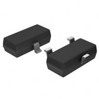
SOT23
Top View
D
Bottom View
D
D
G
G
S
S
S
G
Absolute Maximum Ratings TA=25°C unless otherwise noted
Parameter
Symbol
Drain-Source Voltage
VDS
Gate-Source Voltage
VGS
TA=25°C
Continuous Drain
Current
Pulsed Drain Current
C
Power Dissipation B
Junction and Storage Temperature Range
Thermal Characteristics
Parameter
Maximum Junction-to-Ambient A
Maximum Junction-to-Ambient A D
Maximum Junction-to-Lead
Rev 5: July 2010
Steady-State
Steady-State
A
30
W
0.9
TJ, TSTG
Symbol
t ≤ 10s
V
1.4
PD
TA=70°C
±8
5.2
IDM
TA=25°C
Units
V
6.5
ID
TA=70°C
Maximum
20
RθJA
RθJL
www.aosmd.com
-55 to 150
Typ
70
100
63
°C
Max
90
125
80
Units
°C/W
°C/W
°C/W
Page 1 of 5
�AO3416
Electrical Characteristics (TJ=25°C unless otherwise noted)
Symbol
Parameter
STATIC PARAMETERS
Drain-Source Breakdown Voltage
BVDSS
IDSS
Zero Gate Voltage Drain Current
Conditions
Min
ID=250µA, VGS=0V
TJ=55°C
Gate-Body leakage current
VDS=0V, VGS= ±8V
VDS=VGS ID=250µA
0.4
ID(ON)
On state drain current
VGS=4.5V, VDS=5V
30
±10
1.1
16
22
22
30
VGS=2.5V, ID=5.5A
18
26
mΩ
VGS=1.8V, ID=5A
21
34
mΩ
50
1
V
2
A
1650
pF
TJ=125°C
gFS
Forward Transconductance
VDS=5V, ID=6.5A
VSD
Diode Forward Voltage
IS=1A,VGS=0V
IS
Maximum Body-Diode Continuous Current
DYNAMIC PARAMETERS
Ciss
Input Capacitance
Output Capacitance
Crss
Reverse Transfer Capacitance
Rg
Gate resistance
Gate Source Charge
Qgd
Gate Drain Charge
A
0.62
1295
VGS=0V, VDS=10V, f=1MHz
mΩ
S
160
pF
87
pF
VGS=0V, VDS=0V, f=1MHz
1.8
KΩ
10
nC
VGS=4.5V, VDS=10V, ID=6.5A
4.2
nC
2.6
nC
SWITCHING PARAMETERS
Qg
Total Gate Charge
Qgs
µA
V
0.7
VGS=4.5V, ID=6.5A
Coss
µA
5
Gate Threshold Voltage
Units
V
1
VGS(th)
Static Drain-Source On-Resistance
Max
20
VDS=20V, VGS=0V
IGSS
RDS(ON)
Typ
tD(on)
Turn-On DelayTime
tr
Turn-On Rise Time
tD(off)
Turn-Off DelayTime
tf
Turn-Off Fall Time
trr
Body Diode Reverse Recovery Time
IF=6.5A, dI/dt=100A/µs
31
Qrr
Body Diode Reverse Recovery Charge IF=6.5A, dI/dt=100A/µs
6.8
VGS=4.5V, VDS=10V, RL=1.54Ω,
RGEN=3Ω
280
ns
328
ns
3.76
us
2.24
us
41
ns
nC
A. The value of RθJA is measured with the device mounted on 1in2 FR-4 board with 2oz. Copper, in a still air environment with TA =25°C. The
value in any given application depends on the user's specific board design.
B. The power dissipation PD is based on TJ(MAX)=150°C, using ≤ 10s junction-to-ambient thermal resistance.
C. Repetitive rating, pulse width limited by junction temperature TJ(MAX)=150°C. Ratings are based on low frequency and duty cycles to keep
initialTJ=25°C.
D. The RθJA is the sum of the thermal impedence from junction to lead RθJL and lead to ambient.
E. The static characteristics in Figures 1 to 6 are obtained using
很抱歉,暂时无法提供与“AO3416”相匹配的价格&库存,您可以联系我们找货
免费人工找货- 国内价格
- 10+1.83140
- 200+1.09250
- 800+0.76470
- 3000+0.54620
- 6000+0.51890
- 30000+0.48070
- 国内价格
- 5+0.77910
- 50+0.62916
- 150+0.55419