AOD4184A
40V N-Channel MOSFET
General Description
Product Summary
The AOD4184A combines advanced trench MOSFET
technology with a low resistance package to provide
extremely low RDS(ON). This device is well suited for high
current load applications.
VDS
40V
50A
ID (at VGS=10V)
RDS(ON) (at VGS=10V)
< 7mΩ
RDS(ON) (at VGS = 4.5V)
< 9.5mΩ
100% UIS Tested
100% Rg Tested
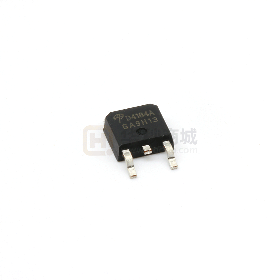
TO252
DPAK
Top View
D
Bottom View
D
D
S
G
G
S
S
G
Absolute Maximum Ratings TA=25°C unless otherwise noted
Symbol
Parameter
VDS
Drain-Source Voltage
VGS
Gate-Source Voltage
Continuous Drain
Current G
TC=25°C
Pulsed Drain Current
C
Avalanche Current C
Avalanche energy L=0.1mH
C
TC=25°C
Power Dissipation
B
TA=25°C
Power Dissipation A
Junction and Storage Temperature Range
Thermal Characteristics
Parameter
Maximum Junction-to-Ambient A
AD
Maximum Junction-to-Ambient
Maximum Junction-to-Case
Rev0 : Sep 2009
IAS, IAR
35
A
EAS, EAR
61
mJ
50
Steady-State
Steady-State
W
25
2.3
RθJA
RθJC
www.aosmd.com
W
1.5
TJ, TSTG
Symbol
t ≤ 10s
A
10
PDSM
TA=70°C
A
13
PD
TC=100°C
V
120
IDSM
TA=70°C
±20
40
IDM
TA=25°C
Continuous Drain
Current
Units
V
50
ID
TC=100°C
Maximum
40
-55 to 175
Typ
18
44
2.4
°C
Max
22
55
3
Units
°C/W
°C/W
°C/W
Page 1 of 6
�AOD4184A
Electrical Characteristics (TJ=25°C unless otherwise noted)
Parameter
Symbol
STATIC PARAMETERS
BVDSS
Drain-Source Breakdown Voltage
IDSS
Zero Gate Voltage Drain Current
Conditions
Min
ID=250µA, VGS=0V
VDS=40V, VGS=0V
5
IGSS
Gate-Body leakage current
VDS=0V, VGS= ±20V
Gate Threshold Voltage
VDS=VGS ID=250µA
1.7
ID(ON)
On state drain current
VGS=10V, VDS=5V
120
VGS=10V, ID=20A
TJ=125°C
VGS=4.5V, ID=15A
±100
nA
2.6
V
5.8
7
9.6
12
7.6
9.5
A
gFS
Forward Transconductance
VDS=5V, ID=5A
37
Diode Forward Voltage
IS=1A,VGS=0V
Maximum Body-Diode Continuous Current
0.7
DYNAMIC PARAMETERS
Ciss
Input Capacitance
Coss
Output Capacitance
Crss
Reverse Transfer Capacitance
Rg
Gate resistance
SWITCHING PARAMETERS
Qg(10V) Total Gate Charge
Qg(4.5V) Total Gate Charge
Qgs
Gate Source Charge
Qgd
Gate Drain Charge
tD(on)
Turn-On DelayTime
tr
Turn-On Rise Time
tD(off)
Turn-Off DelayTime
tf
Turn-Off Fall Time
trr
Qrr
VGS=0V, VDS=20V, f=1MHz
VGS=0V, VDS=0V, f=1MHz
VGS=10V, VDS=20V, ID=20A
Body Diode Reverse Recovery Time
Body Diode Reverse Recovery Charge IF=20A, dI/dt=100A/µs
mΩ
mΩ
S
1
V
20
A
1200
1500
1800
pF
150
215
280
pF
80
135
190
pF
2
3.5
5
Ω
21
27
33
nC
10
14
17
nC
3
5
6
nC
3
6
9
nC
VGS=10V, VDS=20V, RL=1Ω,
RGEN=3Ω
IF=20A, dI/dt=100A/µs
µA
2.1
VSD
IS
Units
V
1
TJ=55°C
Static Drain-Source On-Resistance
Max
40
VGS(th)
RDS(ON)
Typ
6
ns
17
ns
30
ns
17
ns
20
29
38
18
26
34
ns
nC
A. The value of RθJA is measured with the device mounted on 1in 2 FR-4 board with 2oz. Copper, in a still air environment with TA =25°C. The
Power dissipation PDSM is based on R θJA and the maximum allowed junction temperature of 150°C. The value in any given application depends on
the user's specific board design, and the maximum temperature of 175°C may be used if the PCB allows it.
B. The power dissipation PD is based on TJ(MAX)=175°C, using junction-to-case thermal resistance, and is more useful in setting the upper
dissipation limit for cases where additional heatsinking is used.
C. Repetitive rating, pulse width limited by junction temperature TJ(MAX)=175°C. Ratings are based on low frequency and duty cycles to keep initial
TJ =25°C.
D. The RθJA is the sum of the thermal impedence from junction to case R θJC and case to ambient.
E. The static characteristics in Figures 1 to 6 are obtained using
很抱歉,暂时无法提供与“AOD4184A”相匹配的价格&库存,您可以联系我们找货
免费人工找货- 国内价格
- 5+1.97803
- 50+1.55663
- 500+1.16747
- 1000+1.14996
- 2500+0.99656
- 国内价格
- 1+6.60677
- 5+4.39366
- 25+2.62806
- 64+1.74933
- 176+1.65983