AOD4185/AOI4185
P-Channel Enhancement Mode Field Effect Transistor
General Description
Features
The AOD4185/AOI4185 uses advanced trench
technology to provide excellent RDS(ON) and low gate
charge. With the excellent thermal resistance of the
DPAK/IPAK package, this device is well suited for high
current applications.
VDS (V) = -40V
ID = -40A
(VGS = -10V)
RDS(ON) < 15mΩ (VGS = -10V)
RDS(ON) < 20mΩ (VGS = -4.5V)
100% UIS Tested!
100% Rg Tested!
-RoHS Compliant
-Halogen Free*
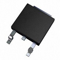
TO252
DPAK
Top View
TO-251A
IPAK
Bottom View
Top View
Bottom View
D
D
D
D
D
G
S
G
S
S
G
G
D
Absolute Maximum Ratings TC=25°C unless otherwise noted
Parameter
Symbol
Drain-Source Voltage
VDS
VGS
Gate-Source Voltage
TC=25°C
Continuous Drain
Current B,H
Pulsed Drain Current
TC=100°C
Avalanche Current C
Power Dissipation B
C
Units
V
±20
V
TA=70°C
D,F
Alpha & Omega Semiconductor, Ltd.
IDM
-115
IAR
-42
mJ
88
31
W
2.5
1.6
TJ, TSTG
-55 to 175
Symbol
t ≤ 10s
Steady-State
Steady-State
A
62.5
PDSM
Junction and Storage Temperature Range
Thermal Characteristics
Parameter
Maximum Junction-to-Ambient A,G
Maximum Junction-to-Ambient A,G
-31
PD
TC=100°C
Maximum Junction-to-Case
D
Maximum
-40
ID
EAR
TA=25°C
Power Dissipation A
S
G
-40
C
Repetitive avalanche energy L=0.1mH
TC=25°C
S
RθJA
RθJC
Typ
15
41
2
°C
Max
20
50
2.4
Units
°C/W
°C/W
°C/W
www.aosmd.com
�AOD4185/AOI4185
Electrical Characteristics (TJ=25°C unless otherwise noted)
Symbol
Parameter
STATIC PARAMETERS
BVDSS
Drain-Source Breakdown Voltage
IDSS
Zero Gate Voltage Drain Current
Conditions
Min
ID=-250µA, VGS=0V
-40
-1
TJ=55°C
-5
IGSS
Gate-Body leakage current
VDS=0V, VGS= ±20V
Gate Threshold Voltage
VDS=VGS ID=-250µA
-1.7
ID(ON)
On state drain current
VGS=-10V, VDS=-5V
-115
±100
VGS=-10V, ID=-20A
Static Drain-Source On-Resistance
TJ=125°C
50
Diode Forward Voltage
IS=-1A,VGS=0V
Maximum Body-Diode Continuous Current
-0.72
DYNAMIC PARAMETERS
Ciss
Input Capacitance
Gate resistance
VGS=0V, VDS=-20V, f=1MHz
VGS=0V, VDS=0V, f=1MHz
SWITCHING PARAMETERS
Qg (-10V) Total Gate Charge
Qg (-4.5V) Total Gate Charge
Qgs
Gate Source Charge
VGS=-10V, VDS=-20V,
ID=-20A
2.5
Units
µA
nA
V
A
20
VSD
Rg
15
23
IS
Reverse Transfer Capacitance
12.5
16
VDS=-5V, ID=-20A
Output Capacitance
-3
19
Forward Transconductance
Crss
-1.9
VGS=-4.5V, ID=-15A
gFS
Coss
Max
V
VDS=-40V, VGS=0V
VGS(th)
RDS(ON)
Typ
mΩ
S
-1
V
-20
A
2550
pF
280
pF
190
pF
4
6
Ω
42
55
nC
18.6
7
nC
Qgd
Gate Drain Charge
8.6
nC
tD(on)
Turn-On DelayTime
9.4
ns
tr
Turn-On Rise Time
20
ns
tD(off)
Turn-Off DelayTime
55
ns
tf
trr
Body Diode Reverse Recovery Time
IF=-20A, dI/dt=100A/µs
38
Qrr
Body Diode Reverse Recovery Charge IF=-20A, dI/dt=100A/µs
47
VGS=-10V, VDS=-20V, RL=1Ω,
RGEN=3Ω
Turn-Off Fall Time
30
ns
49
ns
nC
A: The value of RθJA is measured with the device in a still air environment with T A =25°C. The power dissipation PDSM and current rating IDSM are
based on TJ(MAX)=150°C, using steady state junction-to-ambient thermal resistance.
B. The power dissipation PD is based on TJ(MAX)=175°C, using junction-to-case thermal resistance, and is more useful in setting the upper
dissipation limit for cases where additional heatsinking is used.
C: Repetitive rating, pulse width limited by junction temperature TJ(MAX)=175°C.
D. The RθJA is the sum of the thermal impedence from junction to case RθJC and case to ambient.
E. The static characteristics in Figures 1 to 6 are obtained using
很抱歉,暂时无法提供与“AOD4185”相匹配的价格&库存,您可以联系我们找货
免费人工找货- 国内价格
- 1+2.63340
- 10+2.08890
- 500+1.51470
- 1000+1.28700
- 2500+1.27413
- 25000+1.24865
- 国内价格
- 2500+1.15230
- 12500+1.14070