AOK160A60
600V, a MOS5
TM
N-Channel Power Transistor
General Description
Product Summary
• Proprietary αMOS5TM technology
• Low RDS(ON)
• Optimized switching parameters for better EMI
performance
• Enhanced body diode for robustness and fast reverse
recovery
VDS @ Tj,max
700V
IDM
96A
RDS(ON),max
< 0.16Ω
Qg,typ
46nC
Eoss @ 400V
4.9mJ
Applications
100% UIS Tested
100% Rg Tested
• SMPS with PFC, Flyback and LLC topologies
• Micro inverter with DC/AC inverter topology
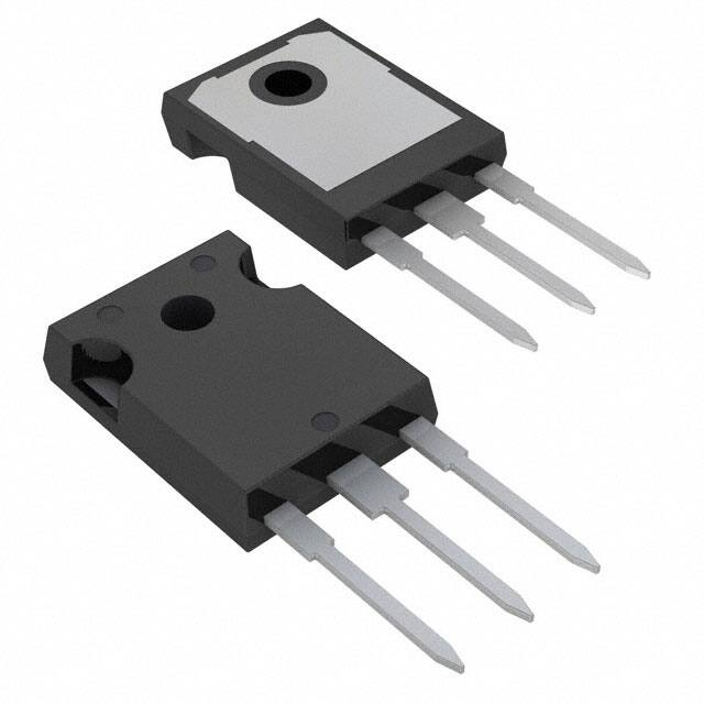
Top View
D
TO-247
G
D
G
S
S
AOK160A60
Orderable Part Number
Package Type
Form
Minimum Order Quantity
AOK160A60
TO247
Tube
240
Absolute Maximum Ratings TA=25°C unless otherwise noted
Parameter
Drain-Source Voltage
Symbol
VDS
Gate-Source Voltage
Gate-Source Voltage (dynamic) AC( f>1Hz)
TC=25°C
Continuous Drain
Current
Pulsed Drain Current
TC=100°C
C
Maximum
600
Units
V
VGS
±20
V
VGS
±30
V
24
ID
15
IDM
A
96
Avalanche Current C
IAR
6
A
Repetitive avalanche energy C
EAR
18
mJ
Single pulsed avalanche energy G
MOSFET dv/dt ruggedness
Peak diode recovery dv/dt
TC=25°C
Power Dissipation B Derate above 25°C
Junction and Storage Temperature Range
Maximum lead temperature for soldering
purpose, 1/8" from case for 5 seconds
EAS
172
100
20
250
2.0
-55 to 150
mJ
W
W/°C
°C
300
°C
Maximum
Units
40
°C/W
0.5
0.5
°C/W
°C/W
Thermal Characteristics
Parameter
Maximum Junction-to-Ambient
Maximum Case-to-sink A
Maximum Junction-to-Case
Rev.3.0: September 2020
A,D
dv/dt
PD
TJ, TSTG
TL
Symbol
RqJA
RqCS
RqJC
www.aosmd.com
V/ns
Page 1 of 6
�AOK160A60
Electrical Characteristics (TJ=25°C unless otherwise noted)
Symbol
Parameter
Conditions
Min
ID=250μA, VGS=0V, TJ=25°C
600
Typ
Max
Units
STATIC PARAMETERS
BVDSS
Drain-Source Breakdown Voltage
BVDSS
/∆TJ
Breakdown Voltage Temperature
Coefficient
IDSS
Zero Gate Voltage Drain Current
IGSS
VGS(th)
Gate-Body leakage current
VDS=0V, VGS=±20V
VDS=5V, ID=250mA
3
RDS(ON)
Gate Threshold Voltage
Static Drain-Source On-Resistance
VGS=10V, ID=12A
0.14
gFS
Forward Transconductance
VDS=10V, ID=12A
VSD
Diode Forward Voltage
IS=12A,VGS=0V
IS
Maximum Body-Diode Continuous Current
ISM
Maximum Body-Diode Pulsed Current C
DYNAMIC PARAMETERS
Ciss
Input Capacitance
Coss
Output Capacitance
Co(er)
Effective output capacitance, energy
related H
Crss
Effective output capacitance, time
I
related
Reverse Transfer Capacitance
Rg
Gate resistance
Co(tr)
ID=250μA, VGS=0V, TJ=150°C
700
ID=250μA, VGS=0V
0.53
V
o
V/ C
VDS=600V, VGS=0V
1
VDS=480V, TJ=125°C
10
±100
nA
0.16
Ω
S
1.2
V
24
A
96
A
V
20
0.87
mA
2340
pF
62
pF
56
pF
233
pF
VGS=0V, VDS=100V, f=1MHz
1.3
pF
f=1MHz
5.4
Ω
46
nC
17
nC
VGS=0V, VDS=100V, f=1MHz
VGS=0V, VDS=0 to 480V, f=1MHz
SWITCHING PARAMETERS
Qg
Total Gate Charge
VGS=10V, VDS=480V, ID=12A
Qgs
Gate Source Charge
Qgd
Gate Drain Charge
14
nC
tD(on)
Turn-On DelayTime
34
ns
tr
Turn-On Rise Time
29
ns
tD(off)
Turn-Off DelayTime
63
ns
tf
trr
Turn-Off Fall Time
19
ns
Body Diode Reverse Recovery Time
387
ns
Irm
Peak Reverse Recovery Current
30
Qrr
Body Diode Reverse Recovery Charge
A
mC
VGS=10V, VDS=400V, ID=12A, RG=5W
IF=12A, dI/dt=100A/ms, VDS=400V
7.3
A. The value of R qJA is measured with the device in a still air environment with T A =25°C.
B. The power dissipation P D is based on TJ(MAX)=150°C, using junction-to-case thermal resistance, and is more useful in setting the upper dissipation
limit for cases where additional heatsinking is used.
C. Repetitive rating, pulse width limited by junction temperature T J(MAX)=150°C, Ratings are based on low frequency and duty cycles to keep initial T J
=25°C.
D. The R qJA is the sum of the thermal impedance from junction to case R qJC and case to ambient.
E. The static characteristics in Figures 1 to 6 are obtained using
很抱歉,暂时无法提供与“AOK160A60”相匹配的价格&库存,您可以联系我们找货
免费人工找货- 国内价格 香港价格
- 1+49.371591+6.38444