AON2403
12V P-Channel MOSFET
General Description
Product Summary
The AON2403 combines advanced trench MOSFET
technology with a low resistance package to provide
extremely low RDS(ON). This device is ideal for load switch
and battery protection applications.
ID (at VGS=-4.5V)
-12V
-8A
VDS
RDS(ON) (at VGS =-4.5V)
< 21mΩ
RDS(ON) (at VGS =-2.5V)
< 28mΩ
RDS(ON) (at VGS =-1.8V)
< 40mΩ
RDS(ON) (at VGS =-1.5V)
< 54mΩ
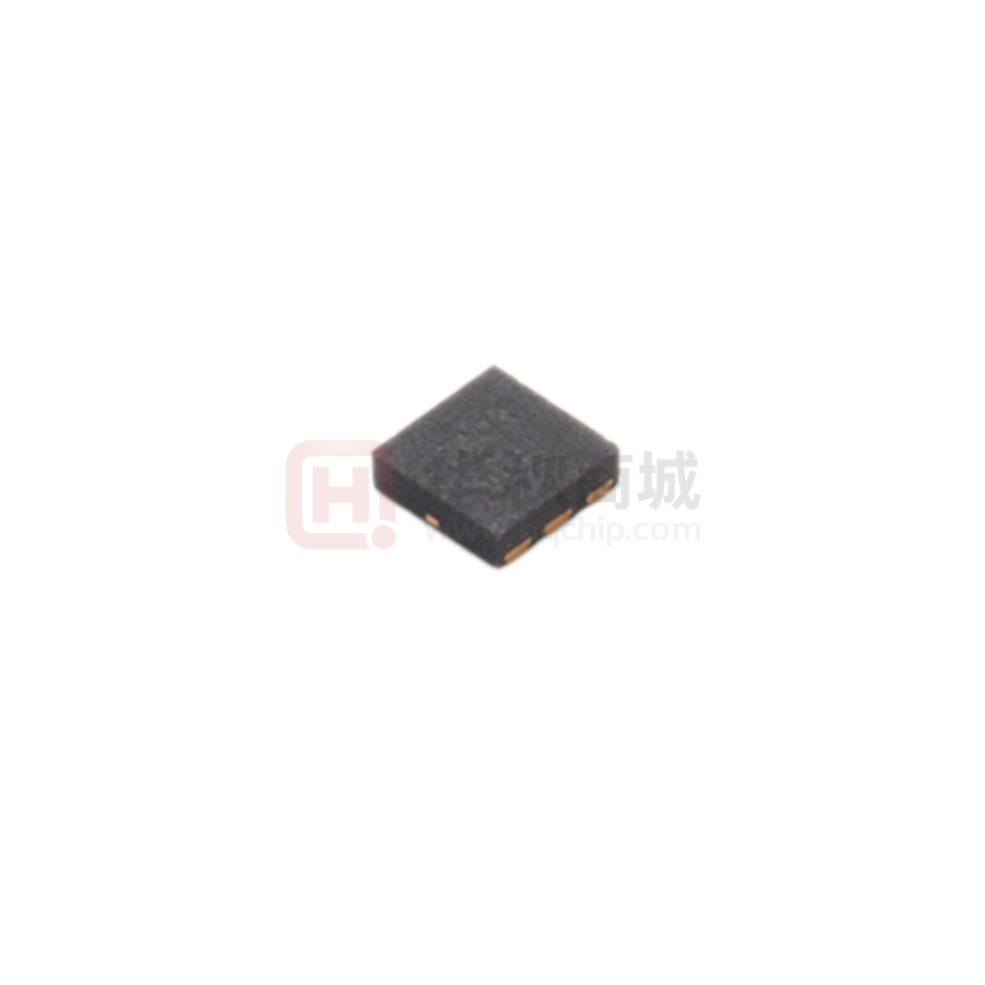
DFN 2x2B
Top View
S
D
Bottom View
D
D
D
Pin 1
S
D
G
Pin 1
G
D
S
Absolute Maximum Ratings TA=25°C unless otherwise noted
Parameter
Symbol
Drain-Source Voltage
VDS
VGS
Gate-Source Voltage
TA=25°C
Continuous Drain
Current G
Pulsed Drain Current
Power Dissipation A
Junction and Storage Temperature Range
Thermal Characteristics
Parameter
Maximum Junction-to-Ambient A
Maximum Junction-to-Ambient A D
Rev 0 : July 2012
Steady-State
A
A
2.8
W
1.8
TJ, TSTG
Symbol
t ≤ 10s
V
-32
PD
TA=70°C
±8
-6
IDM
TA=25°C
Units
V
-8
ID
TA=70°C
C
Maximum
-12
RθJA
www.aosmd.com
-55 to 150
Typ
37
66
°C
Max
45
80
Units
°C/W
°C/W
Page 1 of 5
�AON2403
Electrical Characteristics (TJ=25°C unless otherwise noted)
Symbol
Parameter
STATIC PARAMETERS
BVDSS
Drain-Source Breakdown Voltage
IDSS
Zero Gate Voltage Drain Current
Conditions
Min
ID=-250µA, VGS=0V
-12
-1
TJ=55°C
-5
Gate-Body leakage current
VDS=0V, VGS=±8V
VGS(th)
Gate Threshold Voltage
VDS=VGS, ID=-250µA
-0.3
ID(ON)
On state drain current
VGS=-4.5V, VDS=-5V
-32
VGS=-4.5V, ID=-8A
TJ=125°C
Static Drain-Source On-Resistance
nA
-0.9
V
16.5
21
19.3
25
A
21.5
28
mΩ
VGS=-1.8V, ID=-4A
30
40
mΩ
54
mΩ
VGS=-1.5V, ID=-1A
36
33
VSD
Diode Forward Voltage
IS=-1A,VGS=0V
IS
Maximum Body-Diode Continuous Current
DYNAMIC PARAMETERS
Ciss
Input Capacitance
Reverse Transfer Capacitance
Rg
Gate resistance
VGS=0V, VDS=-6V, f=1MHz
VGS=0V, VDS=0V, f=1MHz
SWITCHING PARAMETERS
Qg
Total Gate Charge
Qgs
Gate Source Charge
mΩ
VGS=-2.5V, ID=-6A
VDS=-5V, ID=-8A
Crss
µA
±100
Forward Transconductance
Output Capacitance
Units
-0.6
gFS
Coss
Max
V
VDS=-12V, VGS=0V
IGSS
RDS(ON)
Typ
-0.6
-1
V
-3.5
A
1370
pF
350
pF
258
pF
10
Ω
12.7
VGS=-4.5V, VDS=-6V, ID=-8A
S
18
nC
1.7
nC
Qgd
Gate Drain Charge
3.4
nC
tD(on)
Turn-On DelayTime
11
ns
tr
Turn-On Rise Time
25
ns
tD(off)
Turn-Off DelayTime
tf
Turn-Off Fall Time
trr
Body Diode Reverse Recovery Time
Qrr
VGS=-4.5V, VDS=-6V, RL=0.75Ω,
RGEN=3Ω
70
ns
41.5
ns
IF=-8A, dI/dt=100A/µs
20.7
Body Diode Reverse Recovery Charge IF=-8A, dI/dt=100A/µs
5.2
ns
nC
A. The value of RθJA is measured with the device mounted on 1in2 FR-4 board with 2oz. Copper, in a still air environment with TA =25°C.
B. The Power dissipation PD is based on R θJA t ≤ 10s value and the maximum allowed junction temperature of 150°C. The value in any given
application depends on the user's specific board design.
C. Repetitive rating, pulse width limited by junction temperature TJ(MAX)=150°C. Ratings are based on low frequency and duty cycles to keep
initial TJ =25°C.
D. The RθJA is the sum of the thermal impedance from junction to case RθJC and case to ambient.
E. The static characteristics in Figures 1 to 6 are obtained using
很抱歉,暂时无法提供与“AON2403”相匹配的价格&库存,您可以联系我们找货
免费人工找货- 国内价格
- 1+2.01570
- 10+1.86060
- 30+1.70560
- 100+1.55050
- 国内价格
- 1+1.14400
- 200+0.87780
- 1500+0.76340
- 3000+0.70950
- 国内价格 香港价格
- 3000+2.111983000+0.27338
- 6000+1.943096000+0.25152
- 9000+1.857069000+0.24038
- 15000+1.7603715000+0.22786
- 21000+1.7031221000+0.22046
- 30000+1.6475030000+0.21326
- 国内价格 香港价格
- 1+8.763471+1.13434
- 10+5.4335710+0.70332
- 100+3.52979100+0.45690
- 500+2.71109500+0.35093
- 1000+2.447311000+0.31678