AON3816 Common-Drain Dual N-Channel Enhancement Mode Field Effect Transistor
General Description
The AON3816/L uses advanced trench technology to provide excellent RDS(ON), low gate charge. It is ESD protected. This device is suitable for use as a unidirectional or bi-directional load switch, facilitated by its common-drain configuration. AON3816 and AO3816L are electrically identical. -RoHS Compliant -AO3816L is Halogen Free
Features
VDS (V) = 20V ID = 4A (VGS = 4.5V) RDS(ON) < 22mΩ (VGS = 4.5V) RDS(ON) < 23mΩ (VGS = 4V) RDS(ON) < 28mΩ (VGS = 2.5V) ESD Protected
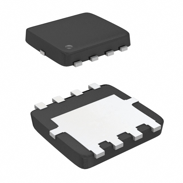
D1 DFN 3x3 Top View Bottom View S2 G2 S1 G1 D2 D2 D1 D1 S1 G1 G2
D2
S2
Absolute Maximum Ratings TA=25°C unless otherwise noted Parameter Drain-Source Voltage Gate-Source Voltage Continuous Drain Current A F Pulsed Drain Current Power Dissipation A
B
Symbol VDS VGS TA=25°C TA=70°C TA=25°C TA=70°C ID IDM PD TJ, TSTG
10 Sec
Steady State
Units V V
20 ±12 4 4 20 2.4 1.5 -55 to 150 1.4 0.9 4 4
A
W °C
Junction and Storage Temperature Range Thermal Characteristics Parameter
Maximum Junction-to-Ambient Maximum Junction-to-Ambient Maximum Junction-to-Lead
C A A
Symbol
t ≤ 10s Steady State Steady State
RθJA RθJL
Typ 43 80 33
Max 52 90 50
Units °C/W °C/W °C/W
Alpha & Omega Semiconductor, Ltd.
www.aosmd.com
�AON3816 Electrical Characteristics (T J=25°C unless otherwise noted) Symbol Parameter Conditions ID=250µA, VGS=0V VDS=20V, VGS=0V TJ=55°C VDS=0V, VGS=±10V VDS=0V, IG=±250µA VDS=VGS ID=250µA VGS=4.5V, VDS=5V VGS=4.5V, ID=4A RDS(ON) Static Drain-Source On-Resistance TJ=125°C VGS=4V, ID=4A VGS=2.5V, ID=4A gFS VSD IS Forward Transconductance VDS=5V, ID=4A IS=1A,VGS=0V Diode Forward Voltage Maximum Body-Diode Continuous Current ±12 0.4 20 14 18 15 17 18 23 19 22.5 21 0.75 1 3 1315 VGS=0V, VDS=10V, f=1MHz VGS=0V, VDS=0V, f=1MHz 219 183 2.1 15 VGS=4.5V, VDS=10V, ID=4A 6.7 4.6 1 VGS=5V, VDS=10V, RL=2.5Ω, RGEN=3Ω
2
Min 20
Typ
Max
Units V
STATIC PARAMETERS BVDSS Drain-Source Breakdown Voltage IDSS IGSS BVGSO VGS(th) ID(ON) Zero Gate Voltage Drain Current Gate-Body leakage current Gate-Source Breakdown Voltage Gate Threshold Voltage On state drain current
1 5 10 0.75 1.1 22 29 23 28
µA µA V V A mΩ mΩ mΩ S V A pF pF pF kΩ nC nC nC µs µs µs µs
DYNAMIC PARAMETERS Ciss Input Capacitance Coss Crss Rg Output Capacitance Reverse Transfer Capacitance Gate resistance
SWITCHING PARAMETERS Qg Total Gate Charge Qgs Gate Source Charge Qgd tD(on) tr tD(off) tf Gate Drain Charge Turn-On DelayTime Turn-On Rise Time Turn-Off DelayTime Turn-Off Fall Time
2.8 5.6 5.9
A: The value of R θJA is measured with the device mounted on 1in FR-4 board with 2oz. Copper, in a still air environment with TA =25°C. The value in any given application depends on the user's specific board design. B: Repetitive rating, pulse width limited by junction temperature. C. The R θJA is the sum of the thermal impedence from junction to lead RθJL and lead to ambient. D. The static characteristics in Figures 1 to 6 are obtained using
很抱歉,暂时无法提供与“AON3816”相匹配的价格&库存,您可以联系我们找货
免费人工找货