AON7442
30V N-Channel AlphaMOS
General Description
Product Summary
• Latest Trench Power AlphaMOS (αMOS LV) technology
• Very Low RDS(on) at 4.5VGS
• Low Gate Charge
• High Current Capability
• RoHS and Halogen-Free Compliant
Application
• DC/DC Converters in Computing, Servers, and POL
• Isolated DC/DC Converters in Telecom and Industrial
VDS
ID (at VGS=10V)
30V
50A
RDS(ON) (at VGS=10V)
< 1.9mΩ
RDS(ON) (at VGS = 4.5V)
< 3.3mΩ
100% UIS Tested
100% Rg Tested
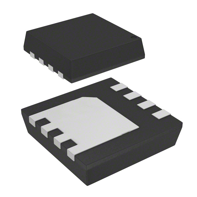
DFN 3.3x3.3 EP
Bottom View
Top View
D
Top View
1
8
2
7
3
6
4
5
G
S
Pin 1
Absolute Maximum Ratings TA=25°C unless otherwise noted
Parameter
Symbol
Drain-Source Voltage
VDS
Gate-Source Voltage
Continuous Drain
CurrentG
VGS
TC=25°C
Pulsed Drain Current C
Continuous Drain
Current
Avalanche Current C
Avalanche energy L=0.05mH
VDS Spike
C
100ns
TC=25°C
Power Dissipation B
TA=25°C
Power Dissipation A
Junction and Storage Temperature Range
Thermal Characteristics
Parameter
Maximum Junction-to-Ambient A
Maximum Junction-to-Ambient A D
Maximum Junction-to-Case
Rev.2.0: January 2016
IAS
66
A
EAS
109
mJ
VSPIKE
36
V
83
Steady-State
Steady-State
W
33
6.2
RθJA
RθJC
www.aosmd.com
W
4
TJ, TSTG
Symbol
t ≤ 10s
A
35
PDSM
TA=70°C
A
44
PD
TC=100°C
V
200
IDSM
TA=70°C
±20
39
IDM
TA=25°C
Units
V
50
ID
TC=100°C
Maximum
30
-55 to 150
Typ
16
45
1.1
°C
Max
20
55
1.5
Units
°C/W
°C/W
°C/W
Page 1 of 6
�AON7442
Electrical Characteristics (TJ=25°C unless otherwise noted)
Symbol
Parameter
STATIC PARAMETERS
Drain-Source Breakdown Voltage
BVDSS
IDSS
Zero Gate Voltage Drain Current
Conditions
Min
ID=250µA, VGS=0V
Gate-Body leakage current
VDS=0V, VGS= ±20V
Gate Threshold Voltage
VDS=VGS,ID=250µA
RDS(ON)
Static Drain-Source On-Resistance
VGS=10V, ID=20A
TJ=125°C
IS=1A,VGS=0V
IS
Maximum Body-Diode Continuous Current G
DYNAMIC PARAMETERS
Ciss
Input Capacitance
Crss
Reverse Transfer Capacitance
Rg
Gate resistance
Qgs
Gate Source Charge
1.9
3.3
mΩ
1
V
50
A
VGS=0V, VDS=0V, f=1MHz
VGS=10V, VDS=15V, ID=20A
0.4
mΩ
S
2994
VGS=0V, VDS=15V, f=1MHz
SWITCHING PARAMETERS
Qg(10V) Total Gate Charge
Qg(4.5V) Total Gate Charge
V
2.9
0.7
Diode Forward Voltage
nA
2.2
1.5
153
Forward Transconductance
VSD
100
2.3
2.4
gFS
Output Capacitance
1.8
VGS=4.5V, ID=20A
VDS=5V, ID=20A
µA
5
1.2
Units
V
1
TJ=55°C
IGSS
Max
30
VDS=30V, VGS=0V
VGS(th)
Coss
Typ
pF
1276
pF
196
pF
0.9
1.4
Ω
47.7
65
nC
23
31
nC
7.6
nC
Qgd
Gate Drain Charge
10
nC
tD(on)
Turn-On DelayTime
10.5
ns
tr
Turn-On Rise Time
tD(off)
Turn-Off DelayTime
tf
Turn-Off Fall Time
trr
Body Diode Reverse Recovery Time
Qrr
7.5
ns
30.8
ns
8.8
ns
IF=20A, dI/dt=500A/µs
20
Body Diode Reverse Recovery Charge IF=20A, dI/dt=500A/µs
46
ns
nC
VGS=10V, VDS=15V, RL=0.75Ω,
RGEN=3Ω
A. The value of RθJA is measured with the device mounted on 1in2 FR-4 board with 2oz. Copper, in a still air environment with TA =25°C. The
Power dissipation PDSM is based on R θJA and the maximum allowed junction temperature of 150°C. The value in any given application depends
on the user's specific board design.
B. The power dissipation PD is based on TJ(MAX)=150°C, using junction-to-case thermal resistance, and is more useful in setting the upper
dissipation limit for cases where additional heatsinking is used.
C. Single pulse width limited by junction temperature TJ(MAX)=150°C.
D. The RθJA is the sum of the thermal impedance from junction to case RθJC and case to ambient.
E. The static characteristics in Figures 1 to 6 are obtained using
很抱歉,暂时无法提供与“AON7442”相匹配的价格&库存,您可以联系我们找货
免费人工找货- 国内价格 香港价格
- 3000+5.555443000+0.71868