AON7804
30V Dual N-Channel MOSFET
General Description
Product Summary
The AON7804 is designed to provide a high efficiency
synchronous buck power stage with optimal layout and
board space utilization. It includes two low RDS (ON)
MOSFETs in a dual DFN3x3 package. The AON7804 is
well suited for use in compact DC/DC converter
applications.
VDS
30V
22A
ID (at VGS=10V)
RDS(ON) (at VGS=10V)
< 21mΩ
RDS(ON) (at VGS = 4.5V)
< 26mΩ
100% UIS Tested
100% Rg Tested
ESD protected
DFN 3x3A_Dual
Bottom View
Top View
D
D
Top View
Pin 1
D1
G1
D1
S2
D2
G2
D2
S1
G
G
Pin 1
S
Absolute Maximum Ratings TA=25°C unless otherwise noted
Parameter
Symbol
VDS
Drain-Source Voltage
VGS
Gate-Source Voltage
TC=25°C
Continuous Drain
Current
Pulsed Drain Current
C
Avalanche Current C
Avalanche energy L=0.1mH
C
TC=25°C
Power Dissipation
B
TA=25°C
Power Dissipation A
Junction and Storage Temperature Range
Thermal Characteristics
Parameter
Maximum Junction-to-Ambient A
AD
Maximum Junction-to-Ambient
Maximum Junction-to-Case
Rev 0: Nov 2010
Steady-State
Steady-State
A
IAS, IAR
19
A
EAS, EAR
18
mJ
17
W
7
3.1
RθJA
RθJC
www.aosmd.com
W
2
TJ, TSTG
Symbol
t ≤ 10s
A
9
PDSM
TA=70°C
V
7
PD
TC=100°C
±20
48
IDSM
TA=70°C
Units
V
14
IDM
TA=25°C
Continuous Drain
Current
Maximum
30
22
ID
TC=100°C
S
-55 to 150
Typ
30
60
6.2
°C
Max
40
75
7.5
Units
°C/W
°C/W
°C/W
Page 1 of 6
�AON7804
Electrical Characteristics (TJ=25°C unless otherwise noted)
Parameter
Symbol
STATIC PARAMETERS
BVDSS
Drain-Source Breakdown Voltage
IDSS
Zero Gate Voltage Drain Current
Conditions
Min
ID=250µA, VGS=0V
VDS=30V, VGS=0V
5
IGSS
Gate-Body leakage current
VDS=0V, VGS= ±20V
Gate Threshold Voltage
VDS=VGS ID=250µA
1.2
ID(ON)
On state drain current
VGS=10V, VDS=5V
48
VGS=10V, ID=8A
TJ=125°C
gFS
Forward Transconductance
VSD
Diode Forward Voltage
IS=1A,VGS=0V
Maximum Body-Diode Continuous Current
IS
DYNAMIC PARAMETERS
Ciss
Input Capacitance
Coss
Output Capacitance
Crss
Reverse Transfer Capacitance
Rg
Gate resistance
SWITCHING PARAMETERS
Qg(10V) Total Gate Charge
Qg(4.5V) Total Gate Charge
Qgs
Gate Source Charge
Qgd
Gate Drain Charge
tD(on)
Turn-On DelayTime
tr
Turn-On Rise Time
tD(off)
Turn-Off DelayTime
tf
Turn-Off Fall Time
trr
Qrr
VGS=0V, VDS=15V, f=1MHz
VGS=0V, VDS=0V, f=1MHz
VGS=10V, VDS=15V, ID=8A
Body Diode Reverse Recovery Time
Body Diode Reverse Recovery Charge IF=8A, dI/dt=500A/µs
µA
V
17
21
A
mΩ
26
mΩ
1
V
15
A
30
0.75
S
600
740
888
pF
77
110
145
pF
50
82
115
pF
0.5
1.1
1.7
Ω
12
15
18
nC
6
7.5
9
nC
VGS=10V, VDS=15V, RL=1.7Ω,
RGEN=3Ω
IF=8A, dI/dt=500A/µs
10
2.4
21
VDS=5V, ID=9A
µA
1.8
23
VGS=4.5V, ID=7A
Units
V
1
TJ=55°C
Static Drain-Source On-Resistance
Max
30
VGS(th)
RDS(ON)
Typ
2.5
nC
3
nC
5
ns
3.5
ns
19
ns
3.5
ns
6
8
10
14
18
22
ns
nC
A. The value of RθJA is measured with the device mounted on 1in 2 FR-4 board with 2oz. Copper, in a still air environment with TA =25°C. The
Power dissipation PDSM is based on R θJA t ≤ 10s value and the maximum allowed junction temperature of 150°C. The value in any given
application depends on the user's specific board design.
B. The power dissipation PD is based on TJ(MAX)=150°C, using junction-to-case thermal resistance, and is more useful in setting the upper
dissipation limit for cases where additional heatsinking is used.
C. Repetitive rating, pulse width limited by junction temperature TJ(MAX)=150°C. Ratings are based on low frequency and duty cycles to keep initial
TJ =25°C.
D. The RθJA is the sum of the thermal impedence from junction to case R θJC and case to ambient.
E. The static characteristics in Figures 1 to 6 are obtained using
很抱歉,暂时无法提供与“AON7804_101”相匹配的价格&库存,您可以联系我们找货
免费人工找货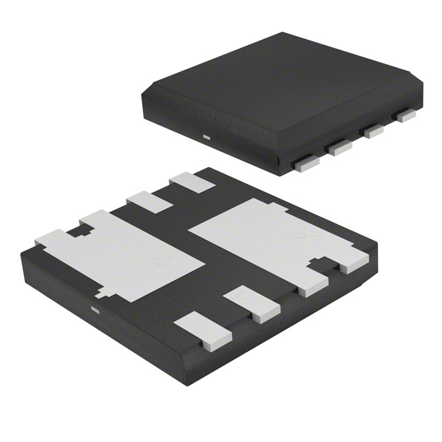


 工商网监
湘ICP备2023018690号
工商网监
湘ICP备2023018690号
