AOSP21321
30V P-Channel MOSFET
General Description
Product Summary
• Latest Advanced Trench Technology
• Low RDS(ON)
• High Current Capability
• RoHS and Halogen-Free Compliant
ID (at VGS=-10V)
VDS
Applications
-30V
-11A
RDS(ON) (at VGS=-10V)
< 17mΩ
RDS(ON) (at VGS=-4.5V)
< 30mΩ
100% UIS Tested
100% Rg Tested
• Notebook AC-in Load Switch
• Battery Protection Charge/Discharge
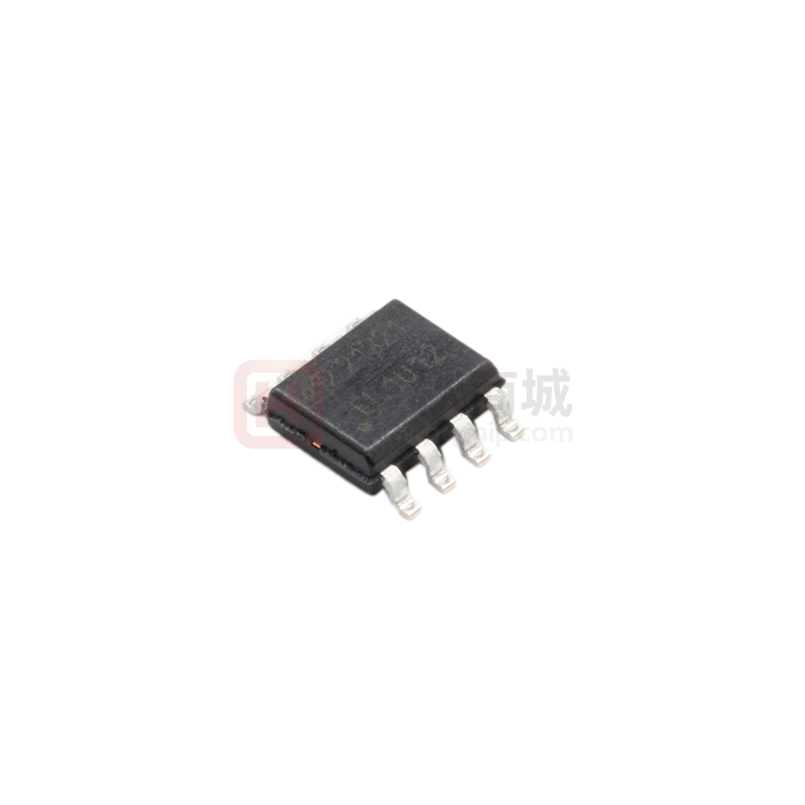
SOIC-8
Top View
D
D
D
Top View
Bottom View
D
D
1
8
2
7
3
6
4
5
G
G
S
S
S
S
Orderable Part Number
Package Type
Form
Minimum Order Quantity
AOSP21321
SO-8
Tape & Reel
3000
Absolute Maximum Ratings TA=25°C unless otherwise noted
Parameter
Drain-Source Voltage
Symbol
VDS
Gate-Source Voltage
VGS
TA=25°C
Continuous Drain
Current
Pulsed Drain Current C
Avalanche energy
L=0.1mH
TA=25°C
Power Dissipation B
TA=70°C
C
Thermal Characteristics
Parameter
Maximum Junction-to-Ambient A
Maximum Junction-to-Ambient A D
Maximum Junction-to-Lead
Rev.1.0: November 2017
Steady-State
Steady-State
A
IAS
25
A
EAS
31
mJ
3.1
W
2.0
TJ, TSTG
Symbol
t ≤ 10s
V
-44
PD
Junction and Storage Temperature Range
±25
-8.5
IDM
Avalanche Current C
Units
V
-11
ID
TA=70°C
Maximum
-30
RθJA
RθJL
-55 to 150
Typ
31
59
16
www.aosmd.com
°C
Max
40
75
24
Units
°C/W
°C/W
°C/W
Page 1 of 5
�AOSP21321
Electrical Characteristics (TJ=25°C unless otherwise noted)
Symbol
Parameter
STATIC PARAMETERS
BVDSS
Drain-Source Breakdown Voltage
Conditions
Min
ID=-250µA, VGS=0V
-30
Typ
Zero Gate Voltage Drain Current
IGSS
VGS(th)
Gate-Body leakage current
VDS=0V, VGS=±25V
Gate Threshold Voltage
VDS=VGS, ID=-250µA
-1
TJ=55°C
±100
nA
-1.8
-2.3
V
14
17
20
24
30
RDS(ON)
Static Drain-Source On-Resistance
VGS=-4.5V, ID=-8A
23.5
gFS
Forward Transconductance
VDS=-5V, ID=-11A
25
VSD
Diode Forward Voltage
IS=-1A, VGS=0V
IS
Maximum Body-Diode Continuous Current
TJ=125°C
DYNAMIC PARAMETERS
Input Capacitance
Ciss
Output Capacitance
Crss
Reverse Transfer Capacitance
Rg
Gate resistance
VGS=0V, VDS=-15V, f=1MHz
f=1MHz
µA
-5
-1.3
VGS=-10V, ID=-11A
Coss
Units
V
VDS=-30V, VGS=0V
IDSS
Max
-0.72
mΩ
mΩ
S
-1
V
-4
A
1180
pF
185
pF
155
pF
5
10
Ω
SWITCHING PARAMETERS
Total Gate Charge
Qg(10V)
21
34
nC
Qg(4.5V)
Total Gate Charge
11
18
Qgs
Gate Source Charge
Qgd
tD(on)
tr
Turn-On Rise Time
tD(off)
Turn-Off DelayTime
tf
trr
Turn-Off Fall Time
IF=-11A, di/dt=500A/µs
Qrr
Body Diode Reverse Recovery Charge IF=-11A, di/dt=500A/µs
15
VGS=-10V, VDS=-15V, ID=-11A
nC
6
nC
Gate Drain Charge
3
nC
Turn-On DelayTime
10.5
ns
Body Diode Reverse Recovery Time
VGS=-10V, VDS=-15V, RL=1.3Ω,
RGEN=3Ω
8.5
ns
30
ns
11.5
ns
10
ns
nC
A. The value of RθJA is measured with the device mounted on 1in2 FR-4 board with 2oz. Copper, in a still air environment with TA =25°C. The
value in any given application depends on the user's specific board design.
B. The power dissipation PD is based on TJ(MAX)=150°C, using ≤ 10s junction-to-ambient thermal resistance.
C. Repetitive rating, pulse width limited by junction temperature TJ(MAX)=150°C. Ratings are based on low frequency and duty cycles to keep
initialTJ=25°C.
D. The RθJA is the sum of the thermal impedance from junction to lead RθJL and lead to ambient.
E. The static characteristics in Figures 1 to 6 are obtained using or equal to -4.5V
Figure 9: Maximum Forward Biased
Safe Operating Area (Note F)
1
1E-05
100
0.001
0.1
10
1000
Pulse Width (s)
Figure 10: Single Pulse Power Rating Junction-toAmbient (Note F)
D=Ton/T
TJ,PK=TA+PDM.ZθJA.RθJA
In descending order
D=0.5, 0.3, 0.1, 0.05, 0.02, 0.01, single pulse
RθJA=75°C/W
0.1
PDM
0.01
0.001
1E-05
Single Pulse
Ton
0.0001
0.001
0.01
0.1
1
10
T
100
1000
Pulse Width (s)
Figure 11: Normalized Maximum Transient Thermal Impedance (Note F)
Rev.1.0: November 2017
www.aosmd.com
Page 4 of 5
�AOSP21321
Gate Charge Test Circuit & Waveform
Vgs
Qg
-10V
-
-
VDC
+
VDC
Qgd
+
DUT
Qgs
Vds
Vgs
Ig
Charge
Resistive Switching Test Circuit & Waveforms
RL
Vds
toff
ton
td(on)
Vgs
-
DUT
Vgs
VDC
td(off)
tr
tf
90%
Vdd
+
Rg
Vgs
10%
Vds
Unclamped Inductive Switching (UIS) Test Circuit & Waveforms
2
L
EAR= 1/2 LIAR
Vds
Vds
Id
-
Vgs
Vgs
VDC
+
Rg
BVDSS
Vdd
Id
I AR
DUT
Vgs
Vgs
Diode Recovery Test Circuit & W aveforms
Q rr = - Idt
Vds +
DUT
Vgs
Vds -
Isd
Vgs
Ig
Rev.1.0: November 2017
L
-Isd
+ Vdd
t rr
dI/dt
-I RM
Vdd
VDC
-
-I F
-Vds
www.aosmd.com
Page 5 of 5
�
很抱歉,暂时无法提供与“AOSP21321”相匹配的价格&库存,您可以联系我们找货
免费人工找货- 国内价格
- 3+2.25306
- 25+1.71884
- 100+1.52121
- 500+1.37148
- 3000+1.27685
- 国内价格
- 5+1.22618
- 50+0.98098
- 150+0.87592