AOT4N60/AOTF4N60/AOTF4N60L
600V,4A N-Channel MOSFET
General Description
Product Summary
The AOT4N60 & AOTF4N60 & AOTF4N60L have been
fabricated using an advanced high voltage MOSFET
process that is designed to deliver high levels of
performance and robustness in popular AC-DC applications.
By providing low RDS(on), Ciss and Crss along with guaranteed
avalanche capability these parts can be adopted quickly into
new and existing offline power supply designs.
VDS
ID (at VGS=10V)
700V@150℃
4A
RDS(ON) (at VGS=10V)
< 2.2W
100% UIS Tested
100% Rg Tested
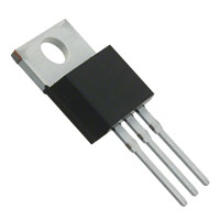
Top View
TO-220
TO-220F
D
D
S
G
G
D
Absolute Maximum Ratings TA=25°C unless otherwise noted
Parameter
Symbol
Drain-Source Voltage
VDS
TC=100°C
C
G
S
AOT4N60
VGS
TC=25°C
Continuous Drain
Current
Pulsed Drain Current
S
AOTF4N60(L)
AOT4N60
Gate-Source Voltage
D
ID
AOTF4N60
600
AOTF4N60L
±30
Units
V
V
4
4*
4*
2.7
2.7*
2.7*
A
IDM
16
Avalanche Current C
IAR
2.5
A
Repetitive avalanche energy C
EAR
94
mJ
Single plused avalanche energy G
MOSFET dv/dt ruggedness
Peak diode recovery dv/dt
TC=25°C
Power Dissipation B Derate above 25oC
Junction and Storage Temperature Range
Maximum lead temperature for soldering
purpose, 1/8" from case for 5 seconds
Thermal Characteristics
Parameter
Maximum Junction-to-Ambient A,D
EAS
188
50
5
35
V/ns
dv/dt
PD
TJ, TSTG
TL
Symbol
RqJA
RqCS
Maximum Case-to-sink A
Maximum Junction-to-Case
RqJC
* Drain current limited by maximum junction temperature.
Rev.12.0: January 2021
104
0.83
0.28
-55 to 150
mJ
25
W
0.20
W/ oC
°C
300
°C
AOT4N60
65
AOTF4N60
65
AOTF4N60L
65
Units
°C/W
0.5
1.2
-3.6
-5
°C/W
°C/W
www.aosmd.com
Page 1 of 6
�AOT4N60/AOTF4N60/AOTF4N60L
Electrical Characteristics (TJ=25°C unless otherwise noted)
Symbol
Parameter
Conditions
Min
ID=250μA, VGS=0V, TJ=25°C
600
Typ
Max
Units
STATIC PARAMETERS
BVDSS
Drain-Source Breakdown Voltage
BVDSS
/∆TJ
Breakdown Voltage Temperature
Coefficient
IDSS
Zero Gate Voltage Drain Current
IGSS
Gate-Body leakage current
VDS=0V, VGS=±30V
VGS(th)
VDS=5V ID=250mA
RDS(ON)
Gate Threshold Voltage
Static Drain-Source On-Resistance
gFS
Forward Transconductance
VSD
Diode Forward Voltage
IS
ISM
ID=250μA, VGS=0V, TJ=150°C
700
ID=250μA, VGS=0V
V
o
V/ C
0.69
VDS=600V, VGS=0V
1
VDS=480V, TJ=125°C
10
±100
mA
4
4.5
nA
V
VGS=10V, ID=2A
1.9
2.2
W
VDS=40V, ID=2A
7.4
IS=1A,VGS=0V
0.77
3
S
1
V
Maximum Body-Diode Continuous Current
4
A
Maximum Body-Diode Pulsed Current
16
A
DYNAMIC PARAMETERS
Ciss
Input Capacitance
Coss
Output Capacitance
Crss
Reverse Transfer Capacitance
Rg
Gate resistance
VGS=0V, VDS=25V, f=1MHz
VGS=0V, VDS=0V, f=1MHz
SWITCHING PARAMETERS
Qg
Total Gate Charge
VGS=10V, VDS=480V, ID=4A
400
511
615
pF
40
51
65
pF
3.5
4.4
5.3
pF
3.3
4.2
6.3
W
15
18
nC
3
3.6
nC
Qgs
Gate Source Charge
Qgd
Gate Drain Charge
7.6
9.1
nC
tD(on)
Turn-On DelayTime
20.2
30
ns
tr
Turn-On Rise Time
28.7
42
ns
tD(off)
Turn-Off DelayTime
36
51
ns
tf
trr
Turn-Off Fall Time
27
40
ns
IF=4A,dI/dt=100A/ms,VDS=100V
212
254
Qrr
Body Diode Reverse Recovery Charge IF=4A,dI/dt=100A/ms,VDS=100V
1.6
1.9
ns
mC
Body Diode Reverse Recovery Time
VGS=10V, VDS=300V, ID=4A,
RG=25W
A. The value of R qJA is measured with the device in a still air environment with T A =25°C.
B. The power dissipation PD is based on TJ(MAX)=150°C, using junction-to-case thermal resistance, and is more useful in setting the upper
dissipation limit for cases where additional heatsinking is used.
C. Repetitive rating, pulse width limited by junction temperature TJ(MAX)=150°C, Ratings are based on low frequency and duty cycles to keep initial
TJ =25°C.
D. The R qJA is the sum of the thermal impedence from junction to case R qJC and case to ambient.
E. The static characteristics in Figures 1 to 6 are obtained using
很抱歉,暂时无法提供与“AOT4N60”相匹配的价格&库存,您可以联系我们找货
免费人工找货- 国内价格
- 1+4.69800
- 200+1.87920
- 500+1.81440
- 1000+1.78200
- 国内价格 香港价格
- 1+15.976961+2.06231
- 50+7.6187350+0.98343
- 100+6.79885100+0.87760
- 500+5.35903500+0.69175
- 1000+4.895561000+0.63192
- 2000+4.505752000+0.58161
- 5000+4.084035000+0.52717
- 10000+3.8235910000+0.49355