AOT8N50/AOTF8N50 500V, 8A N-Channel MOSFET
General Description
The AOT8N50 & AOTF8N50 have been fabricated using an advanced high voltage MOSFET process that is designed to deliver high levels of performance and robustness in popular AC-DC applications. By providing low RDS(on), Ciss and Crss along with guaranteed avalanche capability these parts can be adopted quickly into new and existing offline power supply designs.
Features
VDS (V) = 600V @ 150°C ID = 8A RDS(ON) < 0.85Ω
(VGS = 10V)
100% UIS Tested! 100% R g Tested!
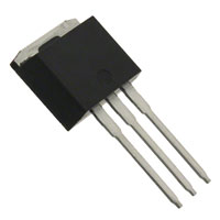
TO-220
Top View
TO-220F
D
G
D
G S
D
G S S
Absolute Maximum Ratings TA=25°C unless otherwise noted Parameter AOT8N50 Symbol AOTF8N50 VDS Drain-Source Voltage 500 VGS ±30 Gate-Source Voltage Continuous Drain Current Pulsed Drain Current Avalanche Current
C C, G C, G
Units V V A A mJ mJ V/ns W W/ oC °C °C
TC=25°C TC=100°C
ID IDM IAR EAR EAS dv/dt PD TJ, TSTG TL Symbol RθJA RθCS
8 5.6 30 3.2 154 307 5 176 1.4 -50 to 150 300 AOT8N50 65 0.5 0.71
8* 5.6*
Repetitive avalanche energy
Single pulsed avalanche energy G Peak diode recovery dv/dt TC=25°C Power Dissipation B Derate above 25 oC Junction and Storage Temperature Range Maximum lead temperature for soldering purpose, 1/8" from case for 5 seconds Thermal Characteristics Parameter Maximum Junction-to-Ambient A,D
A
38.5 0.3
AOTF8N50 65 -3.25
Units °C/W °C/W °C/W
Maximum Case-to-Sink RθJC Maximum Junction-to-Case * Drain current limited by maximum junction temperature.
Alpha & Omega Semiconductor, Ltd.
www.aosmd.com
�AOT8N50/AOTF8N50
Electrical Characteristics (T J=25°C unless otherwise noted) Parameter Symbol STATIC PARAMETERS BVDSS BVDSS /∆TJ IDSS IGSS VGS(th) RDS(ON) gFS VSD IS ISM Drain-Source Breakdown Voltage Breakdown Voltage Temperature Coefficient Zero Gate Voltage Drain Current Gate-Body leakage current Gate Threshold Voltage Static Drain-Source On-Resistance Forward Transconductance Conditions ID=250µA, VGS=0V, TJ=25°C ID=250µA, VGS=0V, TJ=150°C ID=250µA, VGS=0V VDS=500V, VGS=0V VDS=400V, TJ=125°C VDS=0V, VGS=±30V VDS=VGS, ID=250µA VGS=10V, ID=4A VDS=40V, ID=4A 3.4 4 0.63 10 0.73 1 8 30 694 VGS=0V, VDS=25V, f=1MHz VGS=0V, VDS=0V, f=1MHz 74 6.2 2 868 93 7.8 4 23.6 VGS=10V, VDS=400V, ID=8A 5.2 10.6 19.5 VGS=10V, VDS=250V, ID=8A, RG=25Ω IF=8A,dI/dt=100A/µs,VDS=100V 47 51.5 38.5 206 2.14 1042 112 9.4 6.0 28.3 6.2 12.7 323 56.4 62.0 46.0 247.0 2.6 Min 500 600 0.56 1 10 ±100 4.6 0.85 Typ Max Units V V
o V/ C
µA nA V Ω S V A A pF pF pF Ω nC nC nC ns ns ns ns ns µC
Diode Forward Voltage IS=1A, VGS=0V Maximum Body-Diode Continuous Current Maximum Body-Diode Pulsed Current
DYNAMIC PARAMETERS Ciss Input Capacitance Coss Crss Rg Output Capacitance Reverse Transfer Capacitance Gate resistance
SWITCHING PARAMETERS Qg Total Gate Charge Qgs Gate Source Charge Qgd tD(on) tr tD(off) tf trr Qrr Gate Drain Charge Turn-On DelayTime Turn-On Rise Time Turn-Off DelayTime Turn-Off Fall Time
Body Diode Reverse Recovery Time Body Diode Reverse Recovery Charge IF=8A,dI/dt=100A/µs,VDS=100V
A. The value of R θJA is measured with the device in a still air environment with T A =25°C. B. The power dissipation PD is based on TJ(MAX)=150°C, using junction-to-case thermal resistance, and is more useful in setting the upper dissipation limit for cases where additional heatsinking is used. C. Repetitive rating, pulse width limited by junction temperature TJ(MAX)=150°C, Ratings are based on low frequency and duty cycles to keep initial TJ =25°C. D. The R θJA is the sum of the thermal impedence from junction to case R θJC and case to ambient. E. The static characteristics in Figures 1 to 6 are obtained using
很抱歉,暂时无法提供与“AOT8N50”相匹配的价格&库存,您可以联系我们找货
免费人工找货- 国内价格 香港价格
- 1+15.667351+1.96668
- 50+7.4794750+0.93888
- 100+6.68107100+0.83866
- 500+5.27941500+0.66271
- 1000+4.828581000+0.60612
- 2000+4.449362000+0.55852
- 5000+4.039125000+0.50702
- 10000+3.9393510000+0.49450


 工商网监
湘ICP备2023018690号
工商网监
湘ICP备2023018690号