AOTF8T50P
500V,8A N-Channel MOSFET
General Description
Product Summary
• Trench Power AlphaMOS-II technology
• Low RDS(ON)
• Low Ciss and Crss
• High Current Capability
• RoHS and Halogen Free Compliant
VDS @ Tj,max
600V
IDM
32A
RDS(ON),max
< 0.81Ω
Qg,typ
13nC
Eoss @ 400V
2.5µJ
Applications
100% UIS Tested
100% Rg Tested
• General Lighting for LED and CCFL
• AC/DC Power supplies for Industrial, Consumer, and
Telecom
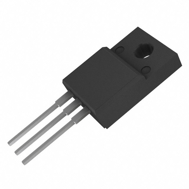
D
Top View
TO-220F
G
G
D
S
S
AOTF8T50P
Orderable Part Number
Package Type
Form
Minimum Order Quantity
AOTF8T50P
AOTF8T50PL
TO-220F Pb Free
TO-220F Green
Tube
Tube
1000
1000
Absolute Maximum Ratings TA=25°C unless otherwise noted
Parameter
Drain-Source Voltage
Symbol
VDS
TC=25°C
Continuous Drain
Current
Avalanche Current C
TC=100°C
C
L=1mH
Repetitive avalanche energy
C
Single pulsed avalanche energy G
MOSFET dv/dt ruggedness
Peak diode recovery dv/dt J
TC=25°C
Power Dissipation B Derate above 25°C
Junction and Storage Temperature Range
Maximum lead temperature for soldering
purpose, 1/8" from case for 5 seconds
ID
±30
Units
V
V
8*
8*
5.4*
5.4*
A
IDM
32
IAR
8
A
EAR
32
mJ
EAS
421
50
15
mJ
dv/dt
PD
V/ns
-55 to 150
W
W/°C
°C
300
°C
38
0.3
TJ, TSTG
28
0.2
TL
Thermal Characteristics
Parameter
Symbol
RθJA
Maximum Junction-to-Ambient A,D
Maximum Junction-to-Case
RθJC
* Drain current limited by maximum junction temperature.
Rev.1.0: July 2014
AOTF8T50PL
500
VGS
Gate-Source Voltage
Pulsed Drain Current
AOTF8T50P
AOTF8T50P
AOTF8T50PL
Units
65
3.3
65
4.5
°C/W
°C/W
www.aosmd.com
Page 1 of 6
�Electrical Characteristics (TJ=25°C unless otherwise noted)
Symbol
Parameter
Conditions
Min
ID=250µA, VGS=0V, TJ=25°C
500
Typ
Max
Units
STATIC PARAMETERS
BVDSS
Drain-Source Breakdown Voltage
BVDSS
/∆TJ
Breakdown Voltage Temperature
Coefficient
IDSS
Zero Gate Voltage Drain Current
ID=250µA, VGS=0V, TJ=150°C
600
ID=250µA, VGS=0V
0.47
VDS=500V, VGS=0V
1
10
Gate-Body leakage current
VDS=0V, VGS=±30V
VDS=5V, ID=250µA
RDS(ON)
VGS=10V, ID=4A
gFS
Forward Transconductance
VDS=40V, ID=4A
6.5
VSD
Diode Forward Voltage
IS=1A,VGS=0V
0.76
IS
ISM
±100
nA
5
V
0.6
0.81
Ω
1
V
Maximum Body-Diode Continuous Current
8
A
Maximum Body-Diode Pulsed Current C
32
A
Coss
Output Capacitance
Co(er)
Effective output capacitance, energy
related H
Crss
Effective output capacitance, time
related I
Reverse Transfer Capacitance
Rg
Gate resistance
VGS=0V, VDS=100V, f=1MHz
Gate Source Charge
S
905
pF
42
pF
31
pF
56
pF
3.5
pF
2
Ω
VGS=0V, VDS=0 to 400V, f=1MHz
VGS=0V, VDS=100V, f=1MHz
f=1MHz
SWITCHING PARAMETERS
Qg
Total Gate Charge
Qgs
3
µA
3.9
DYNAMIC PARAMETERS
Input Capacitance
Ciss
Co(tr)
V/ oC
VDS=400V, TJ=125°C
Gate Threshold Voltage
Static Drain-Source On-Resistance
IGSS
VGS(th)
V
13
VGS=10V, VDS=400V, ID=8A
19
nC
4.4
nC
Qgd
Gate Drain Charge
3.4
nC
tD(on)
Turn-On DelayTime
23
ns
tr
Turn-On Rise Time
33
ns
tD(off)
Turn-Off DelayTime
VGS=10V, VDS=250V, ID=8A,
RG=25Ω
34
ns
tf
trr
Turn-Off Fall Time
21
ns
IF=8A,dI/dt=100A/µs,VDS=100V
340
Qrr
Body Diode Reverse Recovery Charge IF=8A,dI/dt=100A/µs,VDS=100V
3.5
ns
µC
Body Diode Reverse Recovery Time
A. The value of R θJA is measured with the device in a still air environment with T A =25°C.
B. The power dissipation PD is based on TJ(MAX)=150°C, using junction-to-case thermal resistance, and is more useful in setting the upper
dissipation limit for cases where additional heatsinking is used.
C. Repetitive rating, pulse width limited by junction temperature TJ(MAX)=150°C, Ratings are based on low frequency and duty cycles to keep
initial TJ =25°C.
D. The R θJA is the sum of the thermal impedance from junction to case R θJC and case to ambient.
E. The static characteristics in Figures 1 to 6 are obtained using
很抱歉,暂时无法提供与“AOTF8T50P_001”相匹配的价格&库存,您可以联系我们找货
免费人工找货