AOZ1084
1.2A Buck LED Driver
General Description
Features
The AOZ1084 is a high efficiency, simple to use, 1.2A
buck HB LED driver optimized for general lighting
applications. The AOZ1084 works from a 4.5V to 36V
input voltage range, and provides up to 1.2A of
continuous LED current. The 160mV LED current
feedback voltage minimizes the power dissipation of the
external sense resistor. The fixed switching frequency of
450kHz PWM operation reduces inductor and capacitor
sizes.
Up to 36V operating input voltage range
420mΩ internal NMOS
Up to 95% efficiency
Internal compensation
1.2A continuous output current
Fixed 450kHz PWM operation
Internal soft start
160mV LED current feedback voltage with ±8%
accuracy
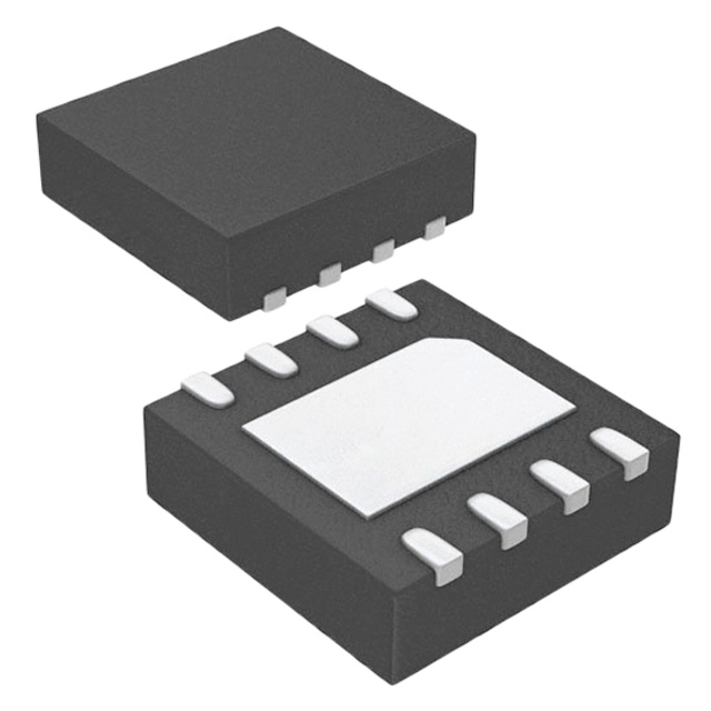
The AOZ1084 is available in a tiny DFN2x2-8L package.
Cycle-by-cycle current limit
Short-circuit protection
Thermal shutdown
Small size DFN2x2-8L
Applications
General LED lighting
Architectural lighting
Signage lighting
Typical Application
VIN
C3
C1
4.7µF
VIN
DIM
BS
AOZ1084
L1
2.2µH
VOUT
LX
LED1
C2
10µF
FB
GND
RS
Figure 1. 1.2A Buck HB LED Driver
Rev. 1.0 June 2015
www.aosmd.com
Page 1 of 12
�AOZ1084
Ordering Information
Part Number
Ambient Temperature Range
Package
Environmental
AOZ1084DI
-40 °C to +85 °C
DFN2x2-8L
Green Product
AOS Green Products use reduced levels of Halogens, and are also RoHS compliant.
Please visit www.aosmd.com/media/AOSGreenPolicy.pdf for additional information.
Pin Configuration
LX
VIN
VIN
DIM
1
8
2
7
3
6
4
5
BST
GND
GND
FB
DFN2x2-8
(Top View)
Pin Description
Pin Number
Pin Name
1
LX
PWM output connection to inductor.
2
VIN
Supply voltage input. Input range from 4.5V to 36V. When VIN rises above the UVLO
threshold the device starts up.
3
VIN
Supply voltage input. Input range from 4.5V to 36V. When VIN rises above the UVLO
threshold the device starts up.
4
DIM
PWM dimming pin. This pin is active high.
5
FB
LED current feedback. The FB pin regulation voltage is 160mV. Connect an external
sense resistor between the cathode of the LED string and GND to set LED current.
6
GND
Ground.
7
GND
Ground.
8
BST
Bootstrap voltage input. High side driver supply. Connected to 10nF capacitor between
BST and LX.
Exposed Pad
EPAD
Rev. 1.0 June 2015
Pin Function
Thermal exposed pad. Pad cam be connected to GND if necessary for improved thermal
performance.
www.aosmd.com
Page 2 of 12
�AOZ1084
Absolute Maximum Ratings
Recommended Operating Conditions
Exceeding the Absolute Maximum Ratings may damage the
device.
The device is not guaranteed to operate beyond the
Recommended Operating Conditions.
Parameter
Rating
Supply Voltage (VVIN)
LX to GND
Parameter
40V
Supply Voltage (VVIN)
4.5V to 36V
-0.7V to VVIN+ 2V
Output Voltage Range
Up to 0.85 * VVIN
DIM to GND
-0.3V to 36V
FB to GND
-0.3V to 6V
VLX + 6V
BST to GND
Junction Temperature (TJ)
+150°C
Storage Temperature (TS)
-65°C to +150°C
ESD Rating
Rating
(1)
Ambient Temperature (TA)
-40°C to +85°C
Package Thermal Resistance (ΘJA)
DFN2x2-8L
55°C/W
2kV
Note:
1. Devices are inherently ESD sensitive, handling precautions are
required. Human body model rating: 1.5kΩ in series with 100pF.
Electrical Characteristics
TA = 25°C, VVIN = 12V, VEN = 12V, unless otherwise specified. Specifications in BOLD indicate a temperature range of -40°C to
+85°C. These specifications are guaranteed by design.
Symbol
VVIN
VUVLO
Parameter
Conditions
Supply Voltage
Input Under-Voltage Lockout Threshold
Min.
4.5
VVIN Rising
VVIN Falling
IVIN
Supply Current (Quiescent)
IOUT = 0, VFB = 1V, VEN > 1.2V
Shutdown Supply Current
VEN = 0V
VFB
Feedback Voltage
TA = 25ºC
IFB
Units
36
V
2.9
V
V
200
IOFF
VFB_LINE
Max.
2.2
UVLO Hysteresis
VFB_LOAD Load Regulation
Typ.
1
147
160
mV
1.5
mA
8
μA
173
mV
120mA < Load < 1.08A
0.5
%
Line Regulation
Load = 600mA
0.03
%/V
Feedback Voltage Input Current
VFB = 160mV
100
nA
PWM DIMMING
VDim_OFF Dimming Input Threshold
VDim_ON
Off Threshold
On Threshold
0.4
1.2
VDim_HYS Dimming Input Hysteresis
IEN
200
Dimming Input Current
V
V
mV
3
μA
540
kHz
MODULATOR
fO
DMAX
TON_MIN
ILIM
Frequency
Maximum Duty Cycle
450
87
Minimum On Time
%
150
Current Limit
Over-Temperature Shutdown Limit
TSS
360
1.5
TJ Rising
TJ Falling
Soft Start Interval
1.9
ns
2.3
A
150
110
°C
°C
600
μs
420
mΩ
POWER STATE OUTPUT
RDS(ON)
NMOS On-Resistance
VIN = 12V
ILEAKAGE
NMOS Leakage
VEN = 0V, VLX = 0V
Rev. 1.0 June 2015
www.aosmd.com
10
μA
Page 3 of 12
�AOZ1084
Block Diagram
VIN
Low Voltage
Regulator
OTP
Detect
Current
Sense
DIM
DIM
Detection
BST
LDO
BST
Softstart
OSC
FB
CLK
–
PWM
Logic
+
0.25V
+
–
Error
Amplifier
OC
Detect
Driver
LX
PWM
Comparator
Short
Detect
GND
Rev. 1.0 June 2015
www.aosmd.com
Page 4 of 12
�AOZ1084
Typical Performance Characteristics
VIN = 12 V, Load = 1 White LED unless otherwise specified.
200Hz Dimming Test (12V/3 LED)
DIM
5V/div
VO
10V/div
VLX
10V/div
ILX
500mA/div
2ms/div
LED Short Test (36V/1 LED)
LED Short Recovery (36V/1 LED)
VO
5V/div
VO
5V/div
VLX
10V/div
VLX
10V/div
ILX
500mA/div
ILX
500mA/div
50μs/div
500μs/div
Normal to LED Open (36V/3 LED)
LED Open to Normal (36V/3 LED)
DIM
5V/div
DIM
5V/div
VO
5V/div
VO
5V/div
VLX
10V/div
VLX
10V/div
ILX
500mA/div
ILX
500mA/div
500μs/div
Rev. 1.0 June 2015
500μs/div
www.aosmd.com
Page 5 of 12
�AOZ1084
Detailed Description
The AOZ1084 is a high efficiency, simple to use, 1.2A
buck HB LED driver optimized for general lighting
applications. Features include enable control, under
voltage lock-out, internal soft-start, output over-voltage
protection, over-current protection and thermal shut
down.
The AOZ1084 is available in a DFN2x2-8L package.
Soft Start and PWM Dimming
LED current can be set by feeding back the output to the
FB pin with the sense resistor RS shown in Figure 1.
The LED current can be programmed as:
0.16
I LED = ----------RS
Protection Features
The AOZ1084 has internal soft start feature to limit
in-rush current and ensure the output voltage ramps up
smoothly to regulation voltage. A soft start process
begins when the input voltage rises to the voltage higher
than UVLO and voltage on Dim pin is HIGH. In soft start
process, the output voltage is ramped to regulation
voltage in typically 600μs. The 600μs soft start time is set
internally.
The DIM pin of the AOZ1084 is active high. Connect the
DIM pin to VIN if enable function is not used. Pull it to
ground will disable the AOZ1084. Do not leave it open.
The voltage on DIM pin must be above 1.2V to enable
the AOZ1084. When voltage on DIM pin falls below 0.4V,
the AOZ1084 is disabled.
Steady-State Operation
Under steady-state conditions, the converter operates in
fixed frequency and Continuous-Conduction Mode
(CCM).
The AOZ1084 integrates an internal NMOS as the highside switch. Inductor current is sensed by amplifying the
voltage drop across the drain to source of the high side
power MOSFET. Output voltage is divided down by the
external voltage divider at the FB pin. The difference of
the FB pin voltage and reference is amplified by the
internal transconductance error amplifier. The error
voltage, is compared against the current signal, which is
sum of inductor current signal and ramp compensation
signal, at PWM comparator input. If the current signal is
less than the error voltage, the internal high-side switch
is on. The inductor current flows from the input through
the inductor to the output. When the current signal
exceeds the error voltage, the high-side switch is off. The
inductor current is freewheeling through the external
Schottky diode to output.
Switching Frequency
The AOZ1084 switching frequency is fixed and set by an
internal oscillator. The switching frequency is set
internally 450kHz.
Rev. 1.0 June 2015
LED Current Programming
The AOZ1084 has multiple protection features to prevent
system circuit damage under abnormal conditions.
Over Current Protection (OCP)
The sensed inductor current signal is also used for over
current protection.
The cycle by cycle current limit threshold is set normal
value of 2A. When the load current reaches the current
limit threshold, the cycle by cycle current limit circuit turns
off the high side switch immediately to terminate the
current duty cycle. The inductor current stop rising. The
cycle by cycle current limit protection directly limits
inductor peak current. The average inductor current is
also limited due to the limitation on peak inductor current.
When cycle by cycle current limit circuit is triggered, the
output voltage drops as the duty cycle decreasing.
The AOZ1084 has internal short circuit protection to
protect itself from catastrophic failure under output short
circuit conditions. As a result, the converter is shut down
and hiccups. The converter will start up via a soft start
once the short circuit condition disappears. In short
circuit protection mode, the inductor average current is
greatly reduced.
UVLO
An UVLO circuit monitors the input voltage. When the
input voltage exceeds 2.9V, the converter starts
operation. When input voltage falls below 2.2V, the
converter will stop switching.
Thermal Protection
An internal temperature sensor monitors the junction
temperature. It shuts down the internal control circuit and
high side NMOS if the junction temperature exceeds
150ºC. The regulator will restart automatically under the
control of soft-start circuit when the junction temperature
decreases to 110°C.
www.aosmd.com
Page 6 of 12
�AOZ1084
Application Information
The basic AOZ1084 application circuit is shown in
Figure 1. Component selection is explained below.
Input Capacitor
The input capacitor must be connected to the VIN pin
and PGND pin of the AOZ1084 to maintain steady input
voltage and filter out the pulsing input current. The
voltage rating of input capacitor must be greater than
maximum input voltage plus ripple voltage.
The input ripple voltage can be approximated by
equation below::
VO VO
IO
ΔV IN = ----------------- × 1 – --------- × --------f × C IN
V IN V IN
Inductor
Since the input current is discontinuous in a buck
converter, the current stress on the input capacitor is
another concern when selecting the capacitor. For a buck
circuit, the RMS value of input capacitor current can be
calculated by:
VO
VO
- 1 – --------
I CIN_RMS = I O × -------V IN
V IN
The inductor is used to supply constant current to output
when it is driven by a switching voltage. For given input
and output voltage, inductance and switching frequency
together decide the inductor ripple current, which is:
VO
VO
-
ΔI L = ----------- × 1 – -------f×L
V IN
The peak inductor current is:
ΔI L
I Lpeak = I O + -------2
if we let m equal the conversion ratio:
VO
-------- = m
V IN
The relationship between the input capacitor RMS
current and voltage conversion ratio is calculated and
shown in Figure 2. It can be seen that when VO is half of
VIN, CIN is under the worst current stress. The worst
current stress on CIN is at 0.5 x IO.
0.5
High inductance gives low inductor ripple current but
requires larger size inductor to avoid saturation. Low
ripple current reduces inductor core losses. It also
reduces RMS current through inductor and switches,
which results in less conduction loss.
When selecting the inductor, make sure it is able to
handle the peak current without saturation even at the
highest operating temperature.
The inductor takes the highest current in a buck circuit.
The conduction loss on inductor needs to be checked for
thermal and efficiency requirements.
0.4
ICIN_RMS(m) 0.3
IO
0.2
Surface mount inductors in different shape and styles are
available from Coilcraft, Elytone and Murata. Shielded
inductors are small and radiate less EMI noise. But they
cost more than unshielded inductors. The choice
depends on EMI requirement, price and size.
0.1
0
For reliable operation and best performance, the input
capacitors must have current rating higher than ICIN-RMS
at worst operating conditions. Ceramic capacitors are
preferred for input capacitors because of their low ESR
and high ripple current rating. Depending on the
application circuits, other low ESR tantalum capacitor or
aluminum electrolytic capacitor may also be used. When
selecting ceramic capacitors, X5R or X7R type dielectric
ceramic capacitors are preferred for their better
temperature and voltage characteristics. Note that the
ripple current rating from capacitor manufactures are
based on certain amount of life time. Further de-rating
may be necessary for practical design requirement.
0
0.5
m
Figure 2. ICIN vs. Voltage Conversion Ratio
Rev. 1.0 June 2015
1
Output Capacitor
The output capacitor is selected based on the DC output
voltage rating, output ripple voltage specification and
ripple current rating.
www.aosmd.com
Page 7 of 12
�AOZ1084
The selected output capacitor must have a higher rated
voltage specification than the maximum desired output
voltage including ripple. De-rating needs to be
considered for long term reliability.
Output ripple voltage specification is another important
factor for selecting the output capacitor. In a buck
converter circuit, output ripple voltage is determined by
inductor value, switching frequency, output capacitor
value and ESR. It can be calculated by the equation
below:
1
ΔV O = ΔI L × ESR CO + -------------------------
8×f×C
O
where,
CO is output capacitor value, and
ESRCO is the equivalent series resistance of the output
capacitor.
When low ESR ceramic capacitor is used as output
capacitor, the impedance of the capacitor at the
switching frequency dominates. Output ripple is mainly
caused by capacitor value and inductor ripple current.
The output ripple voltage calculation can be simplified to:
1
ΔV O = ΔI L × ------------------------8×f×C
O
If the impedance of ESR at switching frequency
dominates, the output ripple voltage is mainly decided by
capacitor ESR and inductor ripple current. The output
ripple voltage calculation can be further simplified to:
ΔV O = ΔI L × ESR CO
For lower output ripple voltage across the entire
operating temperature range, X5R or X7R dielectric type
of ceramic, or other low ESR tantalum capacitor or
aluminum electrolytic capacitor may also be used as
output capacitors.
In a buck converter, output capacitor current is
continuous. The RMS current of output capacitor is
decided by the peak to peak inductor ripple current. It can
be calculated by:
ΔI L
I CO_RMS = ---------12
Thermal Management and Layout
Considerations
In the AOZ1084 buck regulator circuit, high pulsing
current flows through two circuit loops. The first loop
starts from the input capacitors, to the VIN pin, to the LX
pins, to the filter inductor, to the output capacitor and
load, and then return to the input capacitor through
ground. Current flows in the first loop when the high side
switch is on. The second loop starts from inductor, to the
output capacitors and load, to the anode of Schottky
diode, to the cathode of Schottky diode. Current flows in
the second loop when the low side diode is on.
In PCB layout, minimizing the two loops area reduces the
noise of this circuit and improves efficiency. A ground
plane is strongly recommended to connect input
capacitor, output capacitor, and PGND pin of the
AOZ1084.
In the AOZ1084 buck regulator circuit, the major power
dissipating components are the AOZ1084, the Schottky
diode and output inductor. The total power dissipation of
converter circuit can be measured by input power minus
output power:
P total_loss = ( V IN × I IN ) – ( V O × I O )
The power dissipation in the Schottky diode can be
approximated as:
P diode_loss = I O × ( 1 – D ) × V FW_Schottky
where,
VFW_Schottky is the Schottky diode forward voltage
drop.
The power dissipation of the inductor can be
approximately calculated by output current and DCR of
the inductor:
Usually, the ripple current rating of the output capacitor is
a smaller issue because of the low current stress. When
the buck inductor is selected to be very small and
inductor ripple current is high, output capacitor could be
overstressed.
Rev. 1.0 June 2015
The external freewheeling diode supplies the current to
the inductor when the high side NMOS switch is off. To
reduce the losses due to the forward voltage drop and
recovery of diode, Schottky diode is recommended to
use. The maximum reverse voltage rating of the chosen
Schottky diode should be greater than the maximum
input voltage, and the current rating should be greater
than the maximum load current.
P inductor_loss = IO2 × R inductor × 1.1
www.aosmd.com
Page 8 of 12
�AOZ1084
The actual junction temperature can be calculated with
power dissipation in the AOZ1084 and thermal
impedance from junction to ambient.
T junction
= ( P total_loss – P diode_loss – P inductor_loss ) × Θ JA
+ T ambient
The maximum junction temperature of AOZ1084 is
150ºC, which limits the maximum load current capability.
The thermal performance of the AOZ1084 is strongly
affected by the PCB layout. Extra care should be taken
by users during design process to ensure that the IC will
operate under the recommended environmental
conditions.
Several layout tips are listed below for the best electric
and thermal performance.
1. Input capacitor should be connected to the VIN pin
and the GND pin as close as possible.
2. The inductor should be placed as close as possible
the LX pin and the output capacitor.
3. Keep the connection of schottky diode between the
LX pin and the GND pin as short and wide as
possible.
4. Place the feedback resistors and compensation
components as close to the chip as possible.
5. Keep sensitive signal trace far away from the LX pin.
6. Pour a maximized copper area to the VIN pin, the LX
pin and especially the GND pin to help thermal
dissipation.
7. Pour copper plane on all unused board area and
connect it to stable DC nodes, like VIN,GND or
VOUT.
Rev. 1.0 June 2015
www.aosmd.com
Page 9 of 12
�AOZ1084
Package Dimensions, DFN2x2-8L
b
D
E
R
Pin #1 ID
Option 1
E1
E
L
D1
BOTTOM VIEW
TOP VIEW
A
c
Pin #1 ID
Option 2
A1
Seating
Plane
SIDE VIEW
Chamfer
0.2 x 45
BOTTOM VIEW
Dimensions in millimeters
RECOMMENDED LAND PATTERN
0.50
0.25
0.85
0.90
0.30
1.50
UNIT: mm
1.70
Symbols
A
A1
b
c
D
D1
E
E1
e
L
R
aaa
bbb
ccc
ddd
Min.
0.70
0.00
0.18
Nom.
0.75
0.02
0.25
0.20 REF.
2.00 BSC
1.35
1.50
2.00 BSC
0.75
0.90
0.50 BSC
0.20
0.30
0.20
0.15
0.10
0.10
0.08
Max.
0.80
0.05
0.30
1.60
1.00
0.40
Dimensions in inches
Symbols
A
A1
b
c
D
D1
E
E1
e
L
R
aaa
bbb
ccc
ddd
Min. Nom. Max.
0.028 0.030 0.031
0.000 0.001 0.002
0.007 0.010 0.012
0.008 REF.
0.079 BSC
0.053 0.059 0.063
0.079 BSC
0.030 0.035 0.039
0.020 BSC
0.008 0.012 0.016
0.008
0.006
0.004
0.004
0.003
Notes:
1. Dimensions and tolerances conform to ASME Y14.5M-1994.
2. Controlling dimension is millimeter, converted inch dimensions are not necessarily exact.
3. Dimension b applied to metallized terminal and is measured between 0.10mm and 0.30mm from the terminal tip. If the terminal
has the optional radius on the other end of the terminal, dimension b should not be measured in that radius area.
4. Coplanarity ddd applies to the terminals and all other bottom surface metallization.
Rev. 1.0 June 2015
www.aosmd.com
Page 10 of 12
�AOZ1084
Tape and Reel Dimensions, DFN2x2
Carrier Tape
P2
A-A
A
D1
D0
P1
E1
K0
E2
P0
T
A0
Feeding Direction
UNIT: mm
Option
1
2
Package
A0
DFN 2x2 2.25
DFN 2x2A ±0.05
DFN 2x2B 2.30
DFN2x2C ±0.20
E
A
B0
E2
P0
P1
P2
T
2.25
±0.05
B0
1.00
1.50
1.00
8.00
1.75
±0.05 +0.10/-0 +0.25/-0 +0.30/-0.10 ±0.10
K0
D0
D1
3.50
±0.05
4.00
±0.10
4.00
±0.10
2.00
±0.05
0.254
±0.02
2.30
±0.20
1.00
1.50
±0.20 +0.10/-0
3.50
±0.05
4.00
±0.20
4.00
±0.20
2.00
±0.05
0.30
±0.05
1.50
MIN.
E
E1
8.00
1.75
+0.30/-0.10 ±0.10
Reel
W1
S
R
K
M
H
N
UNIT: mm
Tape Size Reel Size
8mm
ø180
M
ø180.0
±0.50
N
60.0
±0.50
W1
8.4
+1.5/-0
H
13.0
±0.20
S
1.5
MIN.
K
13.5
MIN.
R
3.0
±0.50
Leader / Trailer
& Orientation
Trailer Tape
300mm Min.
Rev. 1.0 June 2015
Components Tape
Orientation in Pocket
www.aosmd.com
Leader Tape
500mm Min.
Page 11 of 12
�AOZ1084
Part Marking
AOZ1084DI
(DFN2x2-8)
AU0A
Part Number Code
9 B 12
Week & Year Code
Assembly Location Code
Option Code
Assembly Lot Code
LEGAL DISCLAIMER
Applications or uses as critical components in life support devices or systems are not authorized. AOS does
not assume any liability arising out of such applications or uses of its products. AOS reserves the right to
make changes to product specifications without notice. It is the responsibility of the customer to evaluate suitability
of the product for their intended application. Customer shall comply with applicable legal requirements,
including all applicable export control rules, regulations and limitations.
AOS' products are provided subject to AOS' terms and conditions of sale which are set forth at:
http://www.aosmd.com/terms_and_conditions_of_sale
LIFE SUPPORT POLICY
ALPHA AND OMEGA SEMICONDUCTOR PRODUCTS ARE NOT AUTHORIZED FOR USE AS CRITICAL
COMPONENTS IN LIFE SUPPORT DEVICES OR SYSTEMS.
As used herein:
1. Life support devices or systems are devices or
systems which, (a) are intended for surgical implant into
the body or (b) support or sustain life, and (c) whose
failure to perform when properly used in accordance
with instructions for use provided in the labeling, can be
reasonably expected to result in a significant injury of
the user.
Rev. 1.0 June 2015
2. A critical component in any component of a life
support, device, or system whose failure to perform can
be reasonably expected to cause the failure of the life
support device or system, or to affect its safety or
effectiveness.
www.aosmd.com
Page 12 of 12
�


 工商网监
湘ICP备2023018690号
工商网监
湘ICP备2023018690号
