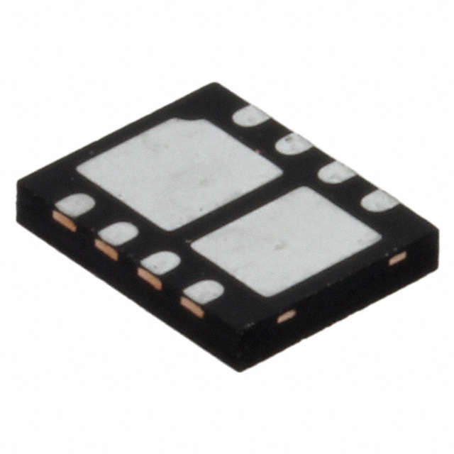
AOZ1092D
EZBuck™ 3A Simple Buck Regulator
General Description
Features
The AOZ1092D is a high efficiency, simple to use, 3A
buck regulator. The AOZ1092D works from a 4.5V to 16V
input voltage range, and provides up to 3A of
continuous output current with an output voltage
adjustable down to 0.8V.
●
4.5V to 16V operating input voltage range
●
50mΩ internal PFET switch for high efficiency:
up to 95%
Schottky diode is included
Internal soft start
Output voltage adjustable to 0.8V
3A continuous output current
Fixed 500kHz PWM operation
Cycle-by-cycle current limit
Short-circuit protection
Output over voltage protection
Thermal shutdown
Small size 4x5 DFN-8 packages
The AOZ1092D comes in 4x5 DFN-8 packages and is
rated over a -40°C to +85°C ambient temperature range.
●
●
●
●
●
●
●
●
●
●
Applications
● Point of load DC/DC conversion
● PCIe graphics cards
● Set top boxes
● DVD drives and HDD
● LCD panels
● Cable modems
● Telecom/networking/datacom equipment
Typical Application
VIN
C1
22µF
Ceramic
VIN
EN
L1
4.7µH
U1
AOZ1092D
COMP
RC
CC
C5
AGND
VOUT
3.3V
LX
R1
C2, C3
22µF
Ceramic
FB
GND
R2
Figure 1. 3.3V/3A Non-Synchronous Buck Regulator
Rev. 1.3 February 2009
www.aosmd.com
Page 1 of 16
�AOZ1092D
Ordering Information
Part Number
Ambient Temperature Range
Package
Environmental
AOZ1092DI
-40°C to +85°C
DFN-8 4x5
RoHS
All AOS Products are offering in packaging with Pb-free plating and compliant to RoHS standards.
Please visit www.aosmd.com/web/quality/rohs_compliant.jsp for additional information.
Pin Configuration
VIN
1
8
LX
7
LX
6
EN
5
COMP
LX
PGND
2
AGND
3
GND
FB
4
4x5 DFN
(Top View)
Pin Description
Pin Number
Pin Name
1
VIN
2
PGND
Power ground. Electrically needs to be connected to AGND.
3
AGND
Reference connection for controller section. Also used as thermal connection for controller section.
Electrically needs to be connected to PGND.
4
FB
5
COMP
6
EN
The enable pin is active HIGH. Connect EN pin to VIN if not used. Do not leave the EN pin floating.
7, 8
LX
PWM output connection to inductor. Thermal connection for output stage.
Rev. 1.3 February 2009
Pin Function
Supply voltage input. When VIN rises above the UVLO threshold the device starts up.
The FB pin is used to determine the output voltage via a resistor divider between the output and
GND.
External loop compensation pin.
www.aosmd.com
Page 2 of 16
�AOZ1092D
Block Diagram
VIN
UVLO
& POR
EN
Internal
+5V
5V LDO
Regulator
OTP
+
ISen
–
Reference
& Bias
Softstart
Q1
ILimit
+
+
0.8V
EAmp
FB
–
–
PWM
Comp
PWM
Control
Logic
+
Level
Shifter
+
FET
Driver
LX
D1
COMP
+
0.2V
0.96V
Frequency
Foldback
Comparator
500kHz/63kHz
Oscillator
–
+
Over Voltage
Protection
Comparator
–
AGND
PGND
Absolute Maximum Ratings
Recommend Operating Ratings
Exceeding the Absolute Maximum Ratings may damage the
device.
The device is not guaranteed to operate beyond the Maximum
Operating Ratings.
Parameter
Supply Voltage (VIN)
Rating
Parameter
18V
Supply Voltage (VIN)
LX to AGND
-0.7V to VIN+0.3V
Output Voltage Range
EN to AGND
-0.3V to VIN+0.3V
Ambient Temperature (TA)
FB to AGND
-0.3V to 6V
COMP to AGND
-0.3V to 6V
PGND to AGND
-0.3V to 0.3V
Junction Temperature (TJ)
+150°C
Storage Temperature (TS)
-65°C to +150°C
Rev. 1.3 February 2009
Package Thermal Resistance
DFN 4x5 (ΘJA)
www.aosmd.com
Rating
4.5V to 16V
0.8V to VIN
-40°C to +85°C
53°C/W
Page 3 of 16
�AOZ1092D
Electrical Characteristics
TA = 25°C, VIN = VEN = 12V, VOUT = 3.3V unless otherwise specified.(3)
Symbol
VIN
VUVLO
Parameter
Conditions
Supply Voltage
Min.
Typ.
4.5
Input Under-Voltage Lockout Threshold
VIN Rising
4.00
VIN Falling
3.70
Max.
Units
16
V
V
Supply Current (Quiescent)
IOUT = 0, VFB = 1.2V, VEN > 1.2V
2
3
mA
IOFF
Shutdown Supply Current
VEN = 0V
1
10
µA
VFB
Feedback Voltage
0.8
0.818
V
IIN
IFB
0.782
Load Regulation
0.5
%
Line Regulation
0.5
%
Feedback Voltage Input Current
200
nA
ENABLE
VEN
EN Input Threshold
Off Threshold
On Threshold
VHYS
0.6
2.0
EN Input Hysteresis
100
V
mV
MODULATOR
Frequency
400
DMAX
Maximum Duty Cycle
100
DMIN
Minimum Duty Cycle
GVEA
Error Amplifier Voltage Gain
500
V/ V
GEA
Error Amplifier Transconductance
200
µA / V
fO
500
600
kHz
%
6
%
PROTECTION
ILIM
Current Limit
4
VPR
Output Over-Voltage Protection Threshold
5
Off Threshold
960
On Threshold
840
A
mV
TJ
Over-Temperature Shutdown Limit
150
°C
tSS
Soft Start Interval
2.2
ms
OUTPUT STAGE
High-Side Switch On-Resistance
VIN = 12V
40
50
VIN = 5V
65
85
mΩ
Note:
3. Specifications in BOLD indicate an ambient temperature range of -40°C to +85°C. These specifications are guaranteed by design.
Rev. 1.3 February 2009
www.aosmd.com
Page 4 of 16
�AOZ1092D
Typical Performance Characteristics
Circuit of Figure 1. TA = 25°C, VIN = VEN = 12V, VOUT = 3.3V unless otherwise specified.
Light Load (DCM) Operation
Full Load (CCM) Operation
Vin ripple
50mV/div
Vin ripple
0.1V/div
Vo ripple
50mV/div
Vo ripple
50mV/div
IL
2A/div
IL
2A/div
VLX
10V/div
VLX
10V/div
1μs/div
1μs/div
Startup to Full Load
Full Load to Turn Off
Vin
5V/div
Vin
5V/div
Vo
2V/div
Vo
1V/div
lin
1A/div
lin
1A/div
400μs/div
1ms/div
50% to 100% Load Transient
No Load to Turn Off
Vin
5V/div
Vo Ripple
0.1V/div
Vo
1V/div
lo
2A/div
1s/div
100μs/div
Rev. 1.3 February 2009
lin
1A/div
www.aosmd.com
Page 5 of 16
�AOZ1092D
Typical Performance Characteristics (Continued)
Circuit of Figure 1. TA = 25°C, VIN = VEN = 12V, VOUT = 3.3V unless otherwise specified.
Short Circuit Protection
Short Circuit Recovery
Vo
2V/div
Vo
2V/div
IL
2A/div
IL
2A/div
100μs/div
1ms/div
Efficiency
Efficiency (VIN = 12V) vs. Load Current
100
8.0V OUTPUT
Efficieny (%)
95
5.0V OUTPUT
90
3.3V OUTPUT
85
80
75
0
0.5
1.0
1.5
2.0
2.5
3.0
Load Current (A)
Thermal Derating Curves
Thermal derating curves for 4x5 DFN-8 package part under typical line and output voltage condition based on
EVAL board. Circuit of Figure 1. 25°C ambient temperature and natural convection (air speed
很抱歉,暂时无法提供与“AOZ1092DIL#A”相匹配的价格&库存,您可以联系我们找货
免费人工找货