物料型号:AOZ1117
器件简介:
AOZ1117是一款低电压降正压可调或固定模式稳压器,具有至少1A的输出电流能力。它专为低电压IC应用设计,如高速总线终端和低电流3.3V逻辑电源的稳定供应。也适用于VGA卡等其他应用。在满载电流时,其电压降低于1.4V,非常适合提供1.25V至5.0V的稳定输出,输入电压范围为2.75V至14V。
特点:
- 最大电压降1.4V
- 快速瞬态响应
- 输出电流限制
- 内置热关断
- 良好的噪声抑制
- 三端可调或固定的1.5V、1.8V、2.5V、3.3V或5.0V输出
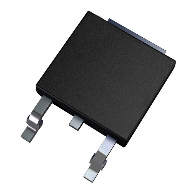
- TO252封装
应用信息:
- 个人电脑外围设备
- 通信
典型电路:
提供了固定输出和可调输出的典型电路示例。
封装信息:
- TO-252封装,带有热沉片连接到输出引脚。
引脚分配:
- 1号引脚:调/地,通过与输出引脚和地之间的电阻分压设置输出电压。
- 2号引脚:输出,稳压器的输出,必须连接至少10μF电容以确保稳定性。
- 3号引脚:输入,稳压器的输入引脚,通常连接一个大储能电容以确保输入电压在负载瞬态响应期间不会下降。
参数特性:
包括绝对最大额定值、推荐操作条件、电气特性等详细参数。
功能详解:
文档提供了详细的功能描述,包括稳压器的工作原理、电气特性和性能特性。
订购信息:
提供了不同输出电压版本的零件编号、环境温度范围、封装类型和环保信息。
电气特性:
在操作条件下的详细电气特性表,包括操作输入电压、参考电压、输出电压、线路调节、负载调节、电压降、电流限制、最小负载电流、纹波抑制、温度稳定性等。
性能特性:
包括负载调节与温度的关系、电压降与输出电流的关系、线路调节、输出电压随温度变化的百分比变化、线路瞬态响应和负载瞬态响应等图表。
封装尺寸:
提供了TO-252-3L封装的详细尺寸图和推荐焊盘图案。
胶带和卷轴尺寸:
提供了胶带和卷轴的尺寸信息。
部件标记:
提供了部件标记的示例和说明。
生命支持政策:
文档声明该产品未授权用于生命支持设备或系统中的关键组件。